This document summarizes a research paper that presents a codec scheme to optimize power in VLSI interconnects using bus encoding. The scheme detects different types of crosstalk couplings between wires and encodes the data to reduce switching activity. It was implemented using Cadence tools in 0.18um technology. Simulation results found a maximum power of 6.44uW for an input combination, showing a 38.89% power reduction over previous work. The scheme models the full custom design approach instead of semi-custom.
Performance Analysis of Full Adder Based 2- Bit Comparator using Different De...IJEEE
In modern digital VLSI design, digital signal processors (DSP) and data processing application-specific integrated circuits(ASIC), comparators are important design element and arithmetic components . In this paper, a 2-bit magnitude comparator has been developed in three different style based on full adder module which is designed to provide good performance. The performance of these three different styles of comparator has been compared in terms of area and power consumption which are the important parameters that are considered while designing any digital circuit. The schematic are designed and simulated for its behavior using DSCH-3.1.The layout of simulated circuits are created using Verilog based netlist file which is then simulated in Microwind 3.1 to analyze the performance of three different styles at 45nm and 90 nm CMOS technology.
Protocol converter (uart, i2 c, manchester protocols to usb)eSAT Journals
Abstract
Abstract now a day’s many industries are using different types of protocols to show data on computer. For this purpose different modules are used which increases the hardware complexity and cost. This project (PROTOCOL CONVERTER) is helpful to overcome these problem different types of protocols such as Manchester, UART and I2Cconverted to the USB format which is compatible to the laptops which is the major application .By using different components such as PIC microcontroller 18F452, LCD, Personal computer, Max 232, DB9 connector.
Keywords::USB (universal serial bus)1, UART(universal asynchronous receiver/transmitter2), I2C (Inter-Integrated Circuit3), Manchester4.
The peer-reviewed International Journal of Engineering Inventions (IJEI) is started with a mission to encourage contribution to research in Science and Technology. Encourage and motivate researchers in challenging areas of Sciences and Technology.
Multiple Valued Logic for Synthesis and Simulation of Digital CircuitsIJERA Editor
The Multiple valued logic(MVL) has increased attention in the last decades because of the possibility to represent the information with more than two discrete levels.Advancing from two-valued to four-valued logic provides a progressive approach. In new technologies, the most delay and power occurs in the connections between gates. When designing a function using MVL, we need fewer gates,which implies less number of connections, then less delay. In the existing system, the 4:1 multiplexer is designed using the MVL logic and various paramaters are analysed. In the proposed system, the idea of designing a Barrel shifter using the multiple valued logic and the parameters are all analyzed. All these designs are verified using Modelsim simulator.
Two innovative high-speed low power parallel 8-bit counter architectures are proposed. Then, High speed 8-bit frequency divider circuits using the proposed architectures are realized. The proposed parallel counter architectures consist of two sections – The Counting Path and the State Excitation Module. The counting path consists of three counting modules in which the first module (basic module) generates future states for the two remaining counting modules. The State Excitation Module decodes the count states of the basic module and carries this decoding over clock cycles through pipelined DFF to trigger the subsequent counting modules. The existing 8-bit parallel counter architecture [1] consumed a total transistor count of 442 whereas the proposed parallel counters consumed only 274 transistors. The power dissipation of the existing parallel counter architecture and the proposed parallel counter architecture were 4.21mW (PINT) and 3.60mW (PINT) respectively at 250MHz. The worst case delay observed for the 8-bit counter using existing parallel counter architecture [1] and the proposed parallel counter architectures were 7.481ns, 6.737ns and 6.677ns respectively using Altera Quartus II. A reduction in area (transistor count) by 27.45% and a reduction in power dissipation by 16.28% are achieved for the frequency dividers using proposed counter architectures. Also a reduction in delay by 10.75% and 7.62% is achieved for the 8-bit frequency divider circuits using proposed counter methods I & II respectively.
VHDL Implementation of Flexible Multiband Dividerijsrd.com
In this paper an efficient multiband flexible divider for Bluetooth, Zigbee and other wireless standards is proposed based on pulse swallow topology and is implemented using Xilinx ISE 13.2 and modalism 6.4c.It consist of a propose wideband multimodulus 32/33/47/48 prescaler, swallow s-counter ,p-counter. As a modification I have implemented a modified multiband flexible divider by combining p and s counters together and by using a modified 2/3 prescaler. Compared to the proposed system modified one will reduce the circuit complexity, power consumption, gate counts etc.
Optimized Layout Design of Priority Encoder using 65nm TechnologyIJEEE
This paper provides comparative performance analysis of power and area of 4 bit priority encoder using 65nm technology.Two priority encoder approaches are presented, one with full automatic and the other with semicustom. The main objective is to compare full automatic and semicustomdesigned layout on the basis of two parameters which is power and area. The automatic design circuit simulation has been done on logic editor and layout created from Verilog file which is simulated. The semicustom layout is created manually and simulated. Creation of layout in both types of method is done at 65nm CMOS technology.The simulation results show that priority encoder using semicustom design has improved power efficiency and area by 29.61µWand 253.8µm2 respectively.
In this paper VLSI design have been introduce decrease the area and power CMOS 90 nm technology is used for designing nor gate. The power consumption and area of nor gate compared in this paper. The proposed design reduces the power consumption and area. The nor gate reduces power consumption by 46% and area by 67% .two design flow are implement, fully automatic and semicustom .the semicustom design better than fully automatic because in this design flow modification is done to minimize the power and area.
Multilevel Inverter using SPWM Technique for AC Power SupplyIJERA Editor
This paper presents two multilevel inverter for AC power supply. The cascaded H bridge topology of multilevel inverter is implemented .The control strategy has been design using SPWM technique. The operation of multilevel inverter is analyzed. The output has controlled and reduction in harmonic and THD. The simulation model has been built in matlab simulink and results are observed.
Development of Distributed Mains Monitoring and Switching System for Indus Co...iosrjce
Indus Complex at Raja Ramanna Centre for Advanced Technology (RRCAT) has two synchrotron
radiation sources, Indus-1 and Indus-2. Microtron is injector to both the machines which sends electron pulses
to the Booster. A new, microcontroller based, distributed mains monitoring and switching system is developed
for Indus complex. It facilitates remote monitoring and switching of AC power switches to various subsystems. It
includes interfacing with power switches/Miniature Circuit Breakers (MCBs) of Indus machine subsystems. This
work involves development of hardware, firmware for microcontroller, implementation of communication
protocol; LabVIEW based server and client application. The developed system allows remote monitoring and
switching of MCBs from main control room.
Arithmetic Operations in Multi-Valued LogicVLSICS Design
This paper presents arithmetic operations like addition, subtraction and multiplications in Modulo-4 arithmetic, and also addition, multiplication in Galois field, using multi-valued logic (MVL). Quaternary to binary and binary to quaternary converters are designed using down literal circuits. Negation in modular arithmetic is designed with only one gate. Logic design of each operation is achieved by reducing the terms using Karnaugh diagrams, keeping minimum number of gates and depth of net in to onsideration. Quaternary multiplier circuit is proposed to achieve required optimization. Simulation result of each operation is shown separately using Hspice.
International Journal of Engineering Research and Applications (IJERA) is an open access online peer reviewed international journal that publishes research and review articles in the fields of Computer Science, Neural Networks, Electrical Engineering, Software Engineering, Information Technology, Mechanical Engineering, Chemical Engineering, Plastic Engineering, Food Technology, Textile Engineering, Nano Technology & science, Power Electronics, Electronics & Communication Engineering, Computational mathematics, Image processing, Civil Engineering, Structural Engineering, Environmental Engineering, VLSI Testing & Low Power VLSI Design etc.
Mixed approach for scheduling process in wimax for high qoseSAT Journals
Abstract
WiMAX(worldwide interoperability for Microwave Access) networks are the networks which are responsible for providing many services like video, data and voice. The WiMAX technology satisfies the modern need of broadband internet through wireless access. For managing all these services through WiMAX, IEEE802.16 gives QOS (Quality of Service) parameter. In WiMAX, a fundamental challenge is to achieve high QOS so that various parameters like waiting time, end to end delay can be minimized and other parameter like execution time and network utilization etc. To obtain high QOS there is scheduling algorithm which is implemented at the base station and subscriber stations. In this paper we discuss scheduling algorithms and also compare the parameters (waiting time, turnaround time, execution time, packet drop age and packet delivery). We purpose a scheduling algorithm which is combination of greedy latency, distance calculation of user from base station, calculate the burst time and apply SJF on that burst values.
Keywords: WiMAX, QOS, IEEE802.16, Scheduling, FCFS (first come first serve), SJF(Shortest job First), Latency.
Low Power Full Adder using 9T Structureidescitation
In this paper, we propose a new 9T 1-bit full adder.
The main objective is full output voltage swing, low power
consumption and temperature sustainability. The proposed
design is more reliable in terms of power consumption, Power
Delay Product (PDP) and temperature sustainability as
compared to the existing full adder designs. The design has
been implemented 45nm technology on Tanner EDA Tool
version 13.0. The simulation results demonstrate the power
consumption, delay and power delay product at different input
voltages ranging 0.4V to 1.4V.
International Journal of Engineering Research and Applications (IJERA) is an open access online peer reviewed international journal that publishes research and review articles in the fields of Computer Science, Neural Networks, Electrical Engineering, Software Engineering, Information Technology, Mechanical Engineering, Chemical Engineering, Plastic Engineering, Food Technology, Textile Engineering, Nano Technology & science, Power Electronics, Electronics & Communication Engineering, Computational mathematics, Image processing, Civil Engineering, Structural Engineering, Environmental Engineering, VLSI Testing & Low Power VLSI Design etc.
NARMA-L2 Controller for Five-Area Load Frequency Controlijeei-iaes
This paper investigates the load-frequency control (LFC) based on neural network for improving power system dynamic performance. In this paper an Artificial Neural Network (ANN)based controller is presented for the Load Frequency Control (LFC) of a five area interconnected power system. The controller is adaptive and is based on a nonlinear auto regressive moving average (NARMA-L2) algorithm. The working of the conventional controller and ANN based NARMA L2 controllers is simulated using MATLAB/SIMULINK package.. The Simulink link results of both the controllers are compared.
Performance analysis of cmos comparator and cntfet comparator designeSAT Publishing House
IJRET : International Journal of Research in Engineering and Technology is an international peer reviewed, online journal published by eSAT Publishing House for the enhancement of research in various disciplines of Engineering and Technology. The aim and scope of the journal is to provide an academic medium and an important reference for the advancement and dissemination of research results that support high-level learning, teaching and research in the fields of Engineering and Technology. We bring together Scientists, Academician, Field Engineers, Scholars and Students of related fields of Engineering and Technology
Design of Quaternary Logical Circuit Using Voltage and Current Mode LogicVLSICS Design
In VLSI technology, designers main concentration were on area required and on performance of the device. In VLSI design power consumption is one of the major concerns due to continuous increase in chip density and decline in size of CMOS circuits and frequency at which circuits are operating. By considering these parameter logical circuits are designed using quaternary voltage mode logic and quaternary current mode logic. Power consumption required for quaternary voltage mode logic is 51.78 % less as compared to binary . Area in terms of number of transistor required for quaternary voltage mode logic is 3 times more as compared to binary. As quaternary voltage mode circuit required large area as compared to quaternary current mode circuit but power consumption required in quaternary voltage mode circuit is less than that required in quaternary current mode circuit.
A NEW DATA ENCODER AND DECODER SCHEME FOR NETWORK ON CHIPEditor IJMTER
System-on-chip (soc) based system has so many disadvantages in power-dissipation as
well as clock rate while the data transfer from one system to another system in on-chip. At the same
time, a higher operated system does not support the lower operated bus network for data transfer.
However an alternative scheme is proposed for high speed data transfer. But this scheme is limited to
SOCs. Unlike soc, network-on-chip (NOC) has so many advantages for data transfer. It has a special
feature to transfer the data in on-chip named as transitional encoder. Its operation is based on input
transitions. At the same time it supports systems which are higher operated frequencies. In this
project, a low-power encoding scheme is proposed. The proposed system yields lower dynamic
power dissipation due to the reduction of switching activity and coupling switching activity when
compared to existing system. Even-though many factors which is based on power dissipation, the
dynamic power dissipation is only considerable for reasonable advantage. The proposed system is
synthesized using quartus II 9.1 software. Besides, the proposed system will be extended up to
interlink PE communication with help of routers and PE’s which are performed by various
operations. To implement this system in real NOC’s contains the proposed encoders and decoders for
data transfer with regular traffic scenarios should be considered.
Comparative Performance Analysis of Low Power Full Adder Design in Different ...ijcisjournal
This paper gives the comparison of performance of full adder design in terms of area, power and delay in
different logic styles. Full adder design achieves low power using the Transmission Gate logic compared to
all other topologies such as Basic CMOS, Pass Transistor and GDI techniques but it make use of more
number of transistors compared to GDI. GDI occupies less area compared to all other logic design styles.
This paper presents the simulated outcome using Tanner tools and also H-Spice tool which shows power
and speed comparison of different full adder designs. All simulations have been performed in 90nm, 45nm
and 22nm scaling parameters using Predictive Technology Models in H-Spice tool.
DESIGN AND IMPLEMENTATION OF BIT TRANSITION COUNTERcsijjournal
In today’s VLSI system design, power consumption is gaining more attention as compared to performance and area. This is due to battery life in portable devices and operating frequency of the design. Power consumption
mainly consists of static power, dynamic power, leakage power and short circuit power. Dynamic power is dominant among all which depends on many factors viz. power supply, load capacitance and frequency. Switching
activity also affects dynamic power consumption of bus which is determined by calculating the number of bit transitions on bus. The purpose of this paper is to design a bit transition counter which can be used to calculate the
switching activity of the circuit nodes. The novel feature is that it can be inserted at any node of the circuit, thus helpful for calculating power consumption of bus.
MODELLING AND SIMULATION OF 128-BIT CROSSBAR SWITCH FOR NETWORK -ONCHIPVLSICS Design
This is widely accepted that Network-on-Chip represents a promising solution for forthcoming complex embedded systems. The current SoC Solutions are built from heterogeneous hardware and Software components integrated around a complex communication infrastructure. The crossbar is a vital component of in any NoC router. In this work, we have designed a crossbar interconnect for serial bit data transfer and 128-parallel bit data transfer. We have shown comparision between power and delay for the serial bit and parallel bit data transfer through crossbar switch. The design is implemented in 0.180 micron TSM technology.The bit rate achived in serial transfer is slow as compared with parallel data transfer. The simulation resuls show that the critical path delay is less for parallel bit data transfer but power dissipation is high.
A COMPARATIVE STUDY OF ULTRA-LOW VOLTAGE DIGITAL CIRCUIT DESIGNVLSICS Design
Ultra-low voltage digital circuit design is an active research area, especially for portable applications such as wearable electronics, intelligent remote sensors, implantable medical devices, and energy-harvesting systems. Due to their application scenarios and circuit components, two major goals for these systems are minimizing energy consumption and improving compatibility with low-voltage power supplies and analog components. The most effective solution to achieve these goals is to reduce the supply voltage, which, however, raises the issue of operability. At ultra-low supply voltages, the integrity of digital signals degrades dramatically due to the indifference between active and leakage currents. In addition, the system timing becomes more unpredictable as the impact of process and supply voltage variations being more significant at lower voltages. This paper presents a comparative study among three techniques for designing digital circuits operating at ultra-low voltages, i.e., Schmitt-triggered gate structure, delayinsensitive asynchronous logic, and Fully-Depleted Silicon-on-Insulator technology. Results show that despite the tradeoffs, all eight combinations of these techniques are viable for designing ultra-low voltage circuits. For a given application, the optimum circuit design can be selected from these combinations based on the lowest voltage, the dynamic range, the power budget, the performance requirement, and the available semiconductor process node.
IJRET : International Journal of Research in Engineering and Technology is an international peer reviewed, online journal published by eSAT Publishing House for the enhancement of research in various disciplines of Engineering and Technology. The aim and scope of the journal is to provide an academic medium and an important reference for the advancement and dissemination of research results that support high-level learning, teaching and research in the fields of Engineering and Technology. We bring together Scientists, Academician, Field Engineers, Scholars and Students of related fields of Engineering and Technology
A review on glitch reduction techniqueseSAT Journals
Abstract This paper presents different techniques for reducing glitch power in digital circuits. The aim of this study is to minimize glitch power as glitch power comes under dynamic power, so that power dissipation will reduce up to some extent in digital circuits. Warren Shum et.al [2011] work shows glitch power in FPGA’s varies from 4 % to 73 % of total dynamic power having an average of 22.6 %. Warren Shum et.al [2011] and J. Lamoureux et.al [2008] motivates us to reduce glitch power in digital circuits as well as FPGA’s. Different techniques are available for reducing glitch power like gate sizing, gate freezing, multiple threshold transistors, hazard filtering, balancing path delay, by reducing switching activity etc. Keywords: Glitch, Power dissipation, Gate sizing, Gate freezing, multiple threshold transistor, Hazard filtering, balancing path delay and switching activity.
IJRET : International Journal of Research in Engineering and Technology is an international peer reviewed, online journal published by eSAT Publishing House for the enhancement of research in various disciplines of Engineering and Technology. The aim and scope of the journal is to provide an academic medium and an important reference for the advancement and dissemination of research results that support high-level learning, teaching and research in the fields of Engineering and Technology. We bring together Scientists, Academician, Field Engineers, Scholars and Students of related fields of Engineering and Technology
Study and implementation of comparator in cmos 50 nm technologyeSAT Journals
Abstract This paper describes the comparator circuits used in FLASH Analog to digital converter (ADC). The performance of FLASH ADC is greatly influenced by the choice of comparator. In this paper, first a single ended “Threshold Inverter Quantizer” (TIQ) is presented. The TIQ comparator is based on a CMOS inverter cell, in which voltage transfer characteristics (VTC) are changed by systematic transistor sizing. However, TIQ comparator is very sensitive to power supply noise. Another comparator circuit presented in this paper is “Two stage open loop comparator”. It is implemented in 50 nm CMOS Technology. Pre-simulation of comparator is done in LT-Spice and post layout simulation is done in Microwind 3.1. Keywords: CMOS, Comparator, TIQ (Threshold Inverter Quantizer), LT-Spice.
An approach to Measure Transition Density of Binary Sequences for X-filling b...IJECEIAES
Switching activity and Transition density computation is an essential stage for dynamic power estimation and testing time reduction. The study of switching activity, transition densities and weighted switching activities of pseudo random binary sequences generated by Linear Feedback shift registers and Feed Forward shift registers plays a crucial role in design approaches of Built-In Self Test, cryptosystems, secure scan designs and other applications. This paper proposed an approach to find transition densities, which plays an important role in choosing of test pattern generator We have analyze conventional and proposed designs using our approache, This work also describes the testing time of benchmark circuits. The outcome of this paper is presented in the form of algorithm, theorems with proofs and analyses table which strongly support the same. The proposed algorithm reduces switching activity and testing time up to 51.56% and 84.61% respectively.
Low power and high performance detff using common feedback inverter logic eSAT Journals
Abstract The power consumption of a system is crucial parameter in modern VLSI circuits especially for low power applications. In this project, a low power Double Edge Triggered D-Flip Flop (DETFF) design is proposed in 65nm CMOS technology. The proposed DETFF is having less number of transistors than earlier designs. Simulations are carried out using HSPICE tool with different clock frequencies ranging from 400MHz to 2GHz and with different supply voltages ranging from 0.8V to 1.2V. In general, a power delay product (PDP)-based comparison is appropriate for low power portable systems. At nominal condition, the PDP of the proposed DETFF is improved by 65.48% and 44.85% over earlier designs DETFF1 and DETFF2 respectively. Simulation results show lowest power dissipation and least delay than existing designs, which claims that the proposed DETFF is suitable for low power and high speed applications. Keywords: CMOS, flip-flops, Double-edge triggered, power dissipation, delay and PDP.
DESIGN AND IMPLEMENTATION OF ANALOG MULTIPLIER WITH IMPROVED LINEARITY VLSICS Design
Analog multipliers are used for frequency conversion and are critical components in modern radio frequency (RF) systems. RF systems must process analog signals with a wide dynamic range at high frequencies. A mixer converts RF power at one frequency into power at another frequency to make signal processing easier and also inexpensive. A fundamental reason for frequency conversion is to allow amplification of the received signal at a frequency other than the RF, or the audio, frequency. This paper deals with two such multipliers using MOSFETs which can be used in communication systems. They were designed and implemented using 0.5 micron CMOS process. The two multipliers were characterized for power consumption, linearity, noise and harmonic distortion. The initial circuit simulated is a basic Gilbert cell whose gain is fairly high but shows more power consumption and high total harmonic distortion. Our paper aims in reducing both power consumption and total harmonic distortion. The second multiplier is a new architecture that consumes 43.07 percent less power and shows 22.69 percent less total harmonic distortion when compared to the basic Gilbert cell. The common centroid layouts of both the circuits have also been developed.
International Journal of Engineering Research and Applications (IJERA) is an open access online peer reviewed international journal that publishes research and review articles in the fields of Computer Science, Neural Networks, Electrical Engineering, Software Engineering, Information Technology, Mechanical Engineering, Chemical Engineering, Plastic Engineering, Food Technology, Textile Engineering, Nano Technology & science, Power Electronics, Electronics & Communication Engineering, Computational mathematics, Image processing, Civil Engineering, Structural Engineering, Environmental Engineering, VLSI Testing & Low Power VLSI Design etc.
Similar to Codec Scheme for Power Optimization in VLSI Interconnects (20)
A survey on Energy Efficient ProtocolsLEACH, Fuzzy-based approach and Neural ...IJEEE
Wireless Sensor Networks (WSN) plays a very important role in transmitting the data from source to destination but energy consumption is one of the major challenges in these networks. WSN consists of hundreds to thousands of nodes which consume energy while transmitting the information and with a span of time whole energy get consumed and network life time gets reduced. Clustering and Cluster head (CH) selection are important parameters used to enhance the lifetime of the WSN. Clustering use two methods: rotating CH periodically in every round to distribute the energy consumption among nodes and the node with more residual energy becomes CH.This research paper is focused on the performance of the techniques used to enhance the energy efficiency in Wireless Sensor Networks (WSNs). Low- Energy Adaptive Clustering Hierarchy (LEACH), Fuzzy- Based and Neural Network are some of the important techniques used. MATLAB simulation tool is considered in this paper.
Implementation of Back-Propagation Neural Network using Scilab and its Conver...IJEEE
Artificial neural network has been widely used for solving non-linear complex tasks. With the development of computer technology, machine learning techniques are becoming good choice. The selection of the machine learning technique depends upon the viability for particular application. Most of the non-linear problems have been solved using back propagation based neural network. The training time of neural network is directly affected by convergence speed. Several efforts are done to improve the convergence speed of back propagation algorithm. This paper focuses on the implementation of back-propagation algorithm and an effort to improve its convergence speed. The algorithm is written in SCILAB. UCI standard data set is used for analysis purposes. Proposed modification in standard backpropagation algorithm provides substantial improvement in the convergence speed.
Automated Air Cooled Three Level Inverter system using ArduinoIJEEE
The output voltage of a three level inverter is stepped voltage in which the output voltage have three possible values. Such systems can be used to interface renewable energy sources with the grid. Temperature has significant effect on performance of power MOSFETs. Typically, the MOSFETs used as power switches in such applications are a significant source of heat, and the heat energy dissipated by these components must be carefully controlled if operating temperatures are to be maintained. So for the system to work efficiently cooling of MOSFETs is required. This paper proposed an automated air cooled 3 level H-bridge inverter. The system consists of MOSFETs, LM 35 temperature sensor, Optocouplers for isolation. Arduino is used to control the on-off operation of fan. When temperature rises above certain level fan turns on to cool the MOSFETs.
In this work, a Split Ring Resonator (SRR) unit cell is simulated in a waveguide with electromagnetic field solver High Frequency Structure Simulator (HFSS). Analytical calculations of the inductance and capacitance have been also carried out to obtain the resonant frequencies for SRR dimensions. A comparison between calculated and simulated resonance frequencies)) is done. A good correlation between simulated and measured resonance frequencies is achieved.
In this paper, we provide the average bit error probabilities of MQAM and MPSK in the presence of log normal shadowing using Maximal Ratio Combining technique for L diversity branches. We have derived probability of density function (PDF) of received signal to noise ratio (SNR) for L diversity branches in Log Normal fadingfor Maximal Ratio Combining (MRC). We have used Fenton-Wilkinson method to estimate the parameters for a single log-normal distribution that approximates the sum of log-normal random variables (RVs). The results that we provide in this paper are an important tool for measuring the performance ofcommunication links in a log-normal shadowing.
An Approach to Speech and Iris based Multimodal Biometric SystemIJEEE
Biometrics is the science and technology of human identification and verification through the use of feature set extracted from the biological data of the individual to be recognized. Unimodal and Multimodal systems are the two modal systems which have been developed so far. Unimodal biometric systems use a single biometric trait but they face limitations in the system performance due to the presence of noise in data, interclass variations and spoof attacks. These problems can be resolved by using multimodal biometrics which rely on more than one biometric information to produce better recognition results. This paper presents an overview of the multimodal biometrics, various fusion levels used in them and suggests the use of iris and speech using score level fusion for a multimodal biometric system.
An Overview of EDFA Gain Flattening by Using Hybrid AmplifierIJEEE
Data communication systems are increasingly engrossing optical fiber communication system as the transmission paths for the information, the information is in the form of light pulses sending from one place to another through the optical fiber. Several types of optical amplifiers have been developed in optical fiber communication system to amplify the optical signals. The erbium doped fiber amplifier is one of the optical fiber amplifiers which are used for long distance communication. The most significant points in any optical amplifier design are gain and noise figure. They are connected to one another. The other optical amplifier, Raman amplifier has wide gain bandwidth. The EDFA gain spectrum has variations over 1536 to 1552 nm, therefore the gain flattening is a research issue in recent years with the development of high capacity DWDM. The gain variation becomes a problem as the number of channels increases. The gain of EDFA depends on large number of device parameters such as, Erbium ion concentration, amplifier length, core radius, pump power. Raman amplifiers can be combined with EDFAs to expand the optical gain flattened bandwidth. This paper focuses on different methods used for the gain flattening.
Design and Implementation of FPGA Based Low Power Pipelined 64 Bit Risc Proce...IJEEE
This paper presents an efficient design and implementation of a 64 bit RISC Processor for Data Logging System. RISC is a design mechanism to reduce the amount of space, time, cost, power and heat etc. reduces the complexity of instruction. The processor is designed for both fixed and floating point number arithmetic calculation. A Data Logger is an electronic instrument that records environmental parameters such as temperature, Humidity, Wind Speed light intensity, water level and water quality. Data Loggers find its key application where automation and control is required. The necessary code written in the hardware description language Verilog HDL.
Design of Image Segmentation Algorithm for Autonomous Vehicle Navigationusing...IJEEE
In the past few years Autonomous vehicles have gained importance due to its widespread applications in the field of civilian and military applications. On-board camera on autonomous vehicles captures the images which need to be processed in real time using the image segmentation algorithm. On board processing of video(frames)in real time is a big challenging task as it involves extracting the information and performing the required operations for navigation.This paper proposes an approach for vision based autonomous vehicle navigation in indoor environment using the designed image segmentation algorithm. The vision based navigation is applied to autonomous vehicle and it is implemented using the Raspberry Pi camera module on Raspberry Pi Model-B+ with the designed image segmentation algorithm. The image segmentation algorithm has been built using smoothing,thresholding, morpho- logical operations, and edge detection. The reference images of directions in the path are detected by the vehicle and accordingly it moves in right or left directions or stops at destination. The vehicle finds the path from source to destination using reference directions. It first captures the video,segments the video(frame by frame), finds the edges in the segmented frame and moves accordingly. The Raspberry Pi also transmits the capture video and segmented results using the Wi-Fi to the remote system for monitoring. The autonomous vehicle is also capable of finding obstacle in its path and the detection is done using the ultrasonic sensors.
Performance Analysis of GSM Network for Different Types of Antennas IJEEE
Today, in metro cities BTSs are increasing day by day and interference is also increasing. This paper shows the received power of the cell depends on a number of factors. Antenna gain and antenna type are one of the important parameters for this. This paper reveals the effect of signal received power by changing the antenna gain and antenna type.The antenna used is omnidirectional and switched beam and gain varies from 5 to 15 dB.The GSM network is simulated for 6 users in Qualnet software.
On the Performance Analysis of Composite Multipath/Shadowing (Weibull-Log Nor...IJEEE
Composite multipath/shadowing fading environments are frequently encountered in different mobile realistic scenarios. These channels are generally modeled differentComposite multipath/shadowing fading. In this paper wepresent the performance analysis of composite (Weibull-Lognormal shadowed) fading. We adopt efficient toolproposed by Holtzman to approximate composite (Weibull-Lognormal shadowed) fading. The performance measures offading communication systems such as Probability densityfunction (PDF) of Signal to Noise ratio (SNR), Amount offading (AF), Outage probability (Pout) and ChannelCapacity(C/B) will be calculated. Graphical results will bepresented for different signals and fading parameters. Thedifferent expressions that will be provided are of greatimportance in assessing the performance of communicationsystems in composite channels.
Design Analysis of Delay Register with PTL Logic using 90 nm TechnologyIJEEE
This paper presents low area and power efficient delay register using CMOS transistors. The proposed register has reduced area than the conventional register. This resistor design consists of 6 NMOS and 6 PMOS. The proposed delay register has been designed in logic editor and simulated using 90nm technology. Also the layout simulation and parametric analysis has been done to find out the results. In this paper register has been designed using full automatic layout design and semicustom layout design. Then the performance of these different designs has been analyzed and compared in terms of power, delay and area. The simulation result shows that circuit design of delay register using PTL techniques improved by power 0.05% and 61.8% area.
Carbon Nanotubes Based Sensor for Detection of Traces of Gas Molecules- A ReviewIJEEE
In this review paper, we discuss various gas sensors based on technique and sensing materials used in there fabrication. Various sensors are designed making use of salient features of carbon nanotubes and its electrical, mechanical, and electromechanical properties. Effect of using nano-composites on sensitivity and selectivity of gas sensor have been studied.
Routing Protocols in Zigbee Based networks: A SurveyIJEEE
ZigBee is the new standard developed wireless personal area network (WPAN) based on IEEE 802.15.4 for low cost, low data rate and low power consumption wireless network. In present times, zigbee has become a hot topic for research and development all over the world. This paper briefly describes various ZigBee network topologies including star, cluster tree and mesh topology and further introduces different ZigBee routing protocols such as AODV, AODVjr, Hierarchical, Integrated and Enhanced hierarchical routing protocol (EHRP).
A Survey of Routing Protocols for Structural Health MonitoringIJEEE
Wireless sensor networks have emerged in recent years as a promising technology that can impact the field of structural monitoring and infrastructure asset management. Various routing protocols are used to define communication among sensor nodes of the wireless sensor network for purpose of disseminating information. These routing protocols can be designed to improve the network performance in terms of energy consumption, delay and security issues. This paper discusses the requirements of routing protocol for Structural health monitoring and presents summary of various routing protocols used for WSNs for Structural health monitoring.
Layout Design Analysis of SR Flip Flop using CMOS TechnologyIJEEE
This paper presents an area, delay and power efficient design of SR flip flop. As the chip manufacturing technology is on the threshold of evaluation, which shrinks a chip in size and enhances its performance, here the flip flop is implemented in a layout level which develops an optimized design using recent CMOS layout tools. The proposed SR flip flop has been designed and simulated using 45nm technology. After that, parametric analysis has been done. In this paper, flip flop has been developed using full automatic design flow and semi-custom design flow. The performance of SR flip flop layouts using different design flows has been analyzed and compared in terms of area, delay and power consumption. The simulation results show that the design of SR flip flop using semi-custom design flow improved the area occupied by 46.9% and power consumption is reduced by 38.4%.
Design of Planar Inverted F-Antenna for Multiband Applications IJEEE
Planar Inverted F- Antenna (PIFA) is widely used in handheld devices because of its various advantages like compact size, good bandwidth and moderate radiation patterns. In this paper, a design of Planar Inverted F- Antenna(PIFA) is proposed that resonates at the frequency of 2.5 GHz with a bandwidth of 300MHz. The relative permittivity of the substrate used is 2.2. The antenna is fed by coaxial feed. Also, gain, VSWR and radiation pattern of the antenna are studied.
Layout Design Analysis of CMOS Comparator using 180nm TechnologyIJEEE
Comparator is a very useful and basic arithmetic component of digital system. In the world of technology the demand of portable devices are increasing day by day. This paper presents CMOS design of 1-bit comparator on 180nm technology. The layout of 1-bit comparator has been developed using Automatic and semi-custom techniques. Both the layouts are compared and analyzed in terms of their Power and Area consumption. Automatic layout is generated from its equivalent schematic whereas semi-custom layout is developed manually. The result shows that semi-custom consumes less power as compared to Automatic.
A Survey on Image Segmentation and its Applications in Image Processing IJEEE
As technology grows day by day computer vision becomes a vital field of understanding the behavior of an image. Image segmentation is a sub field of computer vision that deals with the partition of objects into number of segments. Image segmentation found a huge application in pattern reorganization, texture analysis as well as in medial image processing. This paper focus on distinct sort of image segmentation techniques that are utilized in computer vision. Thus a survey has been created for various image segmentation techniques that describe the importance of the same. Comparison and conclusion has been created within the finish of this paper.
Sachpazis:Terzaghi Bearing Capacity Estimation in simple terms with Calculati...Dr.Costas Sachpazis
Terzaghi's soil bearing capacity theory, developed by Karl Terzaghi, is a fundamental principle in geotechnical engineering used to determine the bearing capacity of shallow foundations. This theory provides a method to calculate the ultimate bearing capacity of soil, which is the maximum load per unit area that the soil can support without undergoing shear failure. The Calculation HTML Code included.
Immunizing Image Classifiers Against Localized Adversary Attacksgerogepatton
This paper addresses the vulnerability of deep learning models, particularly convolutional neural networks
(CNN)s, to adversarial attacks and presents a proactive training technique designed to counter them. We
introduce a novel volumization algorithm, which transforms 2D images into 3D volumetric representations.
When combined with 3D convolution and deep curriculum learning optimization (CLO), itsignificantly improves
the immunity of models against localized universal attacks by up to 40%. We evaluate our proposed approach
using contemporary CNN architectures and the modified Canadian Institute for Advanced Research (CIFAR-10
and CIFAR-100) and ImageNet Large Scale Visual Recognition Challenge (ILSVRC12) datasets, showcasing
accuracy improvements over previous techniques. The results indicate that the combination of the volumetric
input and curriculum learning holds significant promise for mitigating adversarial attacks without necessitating
adversary training.
Hybrid optimization of pumped hydro system and solar- Engr. Abdul-Azeez.pdffxintegritypublishin
Advancements in technology unveil a myriad of electrical and electronic breakthroughs geared towards efficiently harnessing limited resources to meet human energy demands. The optimization of hybrid solar PV panels and pumped hydro energy supply systems plays a pivotal role in utilizing natural resources effectively. This initiative not only benefits humanity but also fosters environmental sustainability. The study investigated the design optimization of these hybrid systems, focusing on understanding solar radiation patterns, identifying geographical influences on solar radiation, formulating a mathematical model for system optimization, and determining the optimal configuration of PV panels and pumped hydro storage. Through a comparative analysis approach and eight weeks of data collection, the study addressed key research questions related to solar radiation patterns and optimal system design. The findings highlighted regions with heightened solar radiation levels, showcasing substantial potential for power generation and emphasizing the system's efficiency. Optimizing system design significantly boosted power generation, promoted renewable energy utilization, and enhanced energy storage capacity. The study underscored the benefits of optimizing hybrid solar PV panels and pumped hydro energy supply systems for sustainable energy usage. Optimizing the design of solar PV panels and pumped hydro energy supply systems as examined across diverse climatic conditions in a developing country, not only enhances power generation but also improves the integration of renewable energy sources and boosts energy storage capacities, particularly beneficial for less economically prosperous regions. Additionally, the study provides valuable insights for advancing energy research in economically viable areas. Recommendations included conducting site-specific assessments, utilizing advanced modeling tools, implementing regular maintenance protocols, and enhancing communication among system components.
CFD Simulation of By-pass Flow in a HRSG module by R&R Consult.pptxR&R Consult
CFD analysis is incredibly effective at solving mysteries and improving the performance of complex systems!
Here's a great example: At a large natural gas-fired power plant, where they use waste heat to generate steam and energy, they were puzzled that their boiler wasn't producing as much steam as expected.
R&R and Tetra Engineering Group Inc. were asked to solve the issue with reduced steam production.
An inspection had shown that a significant amount of hot flue gas was bypassing the boiler tubes, where the heat was supposed to be transferred.
R&R Consult conducted a CFD analysis, which revealed that 6.3% of the flue gas was bypassing the boiler tubes without transferring heat. The analysis also showed that the flue gas was instead being directed along the sides of the boiler and between the modules that were supposed to capture the heat. This was the cause of the reduced performance.
Based on our results, Tetra Engineering installed covering plates to reduce the bypass flow. This improved the boiler's performance and increased electricity production.
It is always satisfying when we can help solve complex challenges like this. Do your systems also need a check-up or optimization? Give us a call!
Work done in cooperation with James Malloy and David Moelling from Tetra Engineering.
More examples of our work https://www.r-r-consult.dk/en/cases-en/
Saudi Arabia stands as a titan in the global energy landscape, renowned for its abundant oil and gas resources. It's the largest exporter of petroleum and holds some of the world's most significant reserves. Let's delve into the top 10 oil and gas projects shaping Saudi Arabia's energy future in 2024.
Final project report on grocery store management system..pdfKamal Acharya
In today’s fast-changing business environment, it’s extremely important to be able to respond to client needs in the most effective and timely manner. If your customers wish to see your business online and have instant access to your products or services.
Online Grocery Store is an e-commerce website, which retails various grocery products. This project allows viewing various products available enables registered users to purchase desired products instantly using Paytm, UPI payment processor (Instant Pay) and also can place order by using Cash on Delivery (Pay Later) option. This project provides an easy access to Administrators and Managers to view orders placed using Pay Later and Instant Pay options.
In order to develop an e-commerce website, a number of Technologies must be studied and understood. These include multi-tiered architecture, server and client-side scripting techniques, implementation technologies, programming language (such as PHP, HTML, CSS, JavaScript) and MySQL relational databases. This is a project with the objective to develop a basic website where a consumer is provided with a shopping cart website and also to know about the technologies used to develop such a website.
This document will discuss each of the underlying technologies to create and implement an e- commerce website.
Codec Scheme for Power Optimization in VLSI Interconnects
1. Int. Journal of Electrical & Electronics Engg. Vol. 2, Spl. Issue 1 (2015) e-ISSN: 1694-2310 | p-ISSN: 1694-2426
NITTTR, Chandigarh EDIT -2015 96
Codec Scheme for Power Optimization in
VLSI Interconnects
1
Dhriti Duggal,2
Rajnish Sharma
1,2
Chitkara University, Himachal Pradesh, India
1
dhriti.duggal@chitkarauniversity.edu.in, 2
rajnish.sharma@chitkarauniversity.edu.in
Abstract— This paper presents a codec scheme for optimizing
power in VLSI Interconnects. It is based on the traditional
bus encoding method which is considered to be one of the
most effective ways of power and delay reduction. The work
done aims at optimizing power by designing the scheme using
Full-Custom design approach. The model has been designed
and implemented using Cadence Virtuoso Analog Design
Suite in 0.18µm CMOS technology. Power has been computed
for different possible combinations of input data. Delay has
been reckoned for the maximum power consuming input
combination. Layout editor has been used to generate the
physical description of the circuit. The 4 bit input data
combination consuming maximum dynamic power of 6.44µW
and propagation delay of 722.7ps is “1000” with previously
transmitted 4 bit data being “0111”. A significant power
reduction of 38.89% has been observed by designing the
scheme using Full-Custom approach as compared to the
conventional Semi-Custom approach of design.
Keywords— Interconnects, Couplings, Power Dissipation,
Layout Implementation.
I. INTRODUCTION
For System on Chip (SOC) and Network on Chip (NOC)
designs in Deep Submicron era, interconnects play an
important role in the overall performance of the chip. They
are used to distribute clock and other signals and to provide
power/ground to and among the various circuits/systems
functions on the chip [1, 2]. Interconnects consume around
44% of the total chip area and hence it becomes very
important to estimate and minimize the power consumed
by them. Coupling Capacitance located between the wire
and its adjacent wires is important to analyze because it
slows down the signal. It can become the major component
of delay if the switching and coupling activities between
the group wires are not minimized. Further it may also lead
to Crosstalk and Signal Integrity related issues, which in
the worst of the cases may lead to the complete circuit
malfunction if not modeled properly [3-6]. There are
various methods to reduce the crosstalk, power
consumption and propagation delay but bus encoding
method is one of the most efficient methods [3]. It reduces
power consumption and crosstalk by bringing reduction in
the switching activity that is by reducing the number of
power consuming voltage transitions experienced by the
output capacitance/clock cycle.
Power consumption sources in digital CMOS circuits are
broadly classified into three main categories: static, short-
circuit and dynamic power dissipation [7]. Dynamic power
dissipation is one of the most dominant sources of power
dissipation in CMOS circuits which cannot be ignored.
Thus, to optimize power in any design successfully,
dynamic power has to be estimated and minimized
separately. The dissipated power is expressed as:
Pdiss = α* VDD
2
* fCLK* CL (1)
Where, CL is the load capacitance, VDD is supply voltage,
fCLK is the clock frequency and α is the average activity
factor or the switching factor whose value lies between 0
and 1. This paper focuses on bus encoding method for
reducing power dissipation of VLSI Interconnects by
reducing the switching activity.
The rest of the paper is organized as follows: Section II
discusses the types of couplings in interconnects. Section
III describes the implemented codec scheme. Results have
been discussed in Section IV and Section V concludes the
paper.
II. COUPLINGS IN INTERCONNECTS
The coupling between groups of three wires is classified
into five types depending upon the nature of transitions of
signals in the wires that are Type-0, Type-1, Type-2, Type-
3 and Type-4 as shown in Table 1 [3-6].
Table I. 3 bit bus couplings
TYPE-0 TYPE-1 TYPE-2 TYPE-3 TYPE-4
˗ ˗ ˗ ˗ ˗↑ ˗ ↑ ˗ ˗ ↑↓ ↑↓↑
↑↑↑ ˗↑↑ ↑↑ ˗ ˗ ↓↑ ↓↑↓
↓↓↓ ↑˗ ˗ ↑ ˗ ↓ ↑↓ ˗
↑↑˗ ↑↑↓ ↓↑ ˗
˗ ˗↓ ↑↓↓
˗↓↓ ˗ ↓ ˗
˗ ˗↓ ↓ ˗ ↓
↓↓ ˗ ↓ ˗ ↑
↓↓↑
↓↑↑
↑: transition from 0 to 1; ↓: transition from 1 to 0; ˗: no transition
Type-0 coupling occurs when all the 3 bit wires undergo
the same transition [1-2].Type-1 coupling occurs when
there is transition in one or maximum two wires (including
the centre one) while the third wire remains quite [1-
2].Type-2 coupling occurs when the centre wire is in the
opposite state transition with one of its adjacent wires
while the other wire undergoes the same state transition as
the centre wire [1-2]. Type-3 coupling occurs when the
centre wire undergoes the opposite state transition with one
of the two wires while the other wires are quite[1-2].Type-
4 coupling occurs when all the three wire transitions in the
opposite state with respect to each other[1-2].
III. IMPLEMENTED CODEC SCHEME
Fig 1 shows the block diagram of the implemented codec
scheme. Transition Detector compares the present 4 bit
input data with the previously transmitted 4 bit data.
Output of the transition detector acts as an input to the
coupling detectors which help in detecting crosstalk
couplings. XOR Stacks are used at both the encoder and
decoder side to transmit and receive data.
2. Int. Journal of Electrical & Electronics Engg. Vol. 2, Spl. Issue 1 (2015) e-ISSN: 1694-2310 | p-ISSN: 1694-2426
97 NITTTR, Chandigarh EDIT-2015
Fig. 1 Block Diagram of the implemented codec scheme
Layout of different blocks of the implemented codec
scheme are shown in the figures below:
Fig 2 shows the layout of the transition detector which acts
as a comparator and is used to compare the 4 bit present
input data with previously transmitted 4 bit data on the
same data lines. The combination of first four NOT and
AND gates are used to detect ‘low’ to ‘high’ transitions on
the data bus whereas the combination of last four NOT and
AND gates are used to detect ‘high’ to ‘low’ transitions on
the data bus.
Fig. 2 Layout of Transition Detector
8 bit output of the transition detector acts as an input to the
coupling detectors where type-0, type-1, type-2, type-3 and
type-4 coupling detector individually are used to detect the
occurrence of any of the types of type-0, type-1,type-
2,type-3 and type-4 crosstalk couplings. Further it
generates a 1 bit output signal. If any of the output signal is
‘high’ it indicates the occurrence of that particular
crosstalk coupling else not. Fig 3 shows the layout of type-
2 coupling detector which covers the maximum number of
coupling cases as explained in table I. Similar ways,
layouts of all other coupling detectors have been designed.
Fig. 3 Layout of Type-2 Coupling Detector
1 bit output of the individual coupling detectors acts as an
input to the 5 input OR gate which is used to generate the
desired 1 bit control signal as shown in fig 4. If its output
is ‘high’ then the inverted data is sent to the output side
using XOR stack 1 and if its output is ‘low’ then the
original data is sent to the output side using XOR stack 1.
Fig. 4 Layout of 5 Input OR gate
3. Int. Journal of Electrical & Electronics Engg. Vol. 2, Spl. Issue 1 (2015) e-ISSN: 1694-2310 | p-ISSN: 1694-2426
NITTTR, Chandigarh EDIT -2015 98
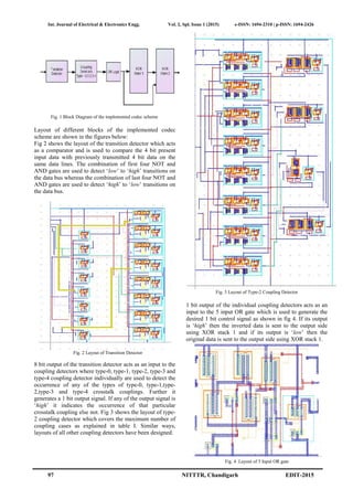
Fig 5 shows XOR Stack 1 which is used to transmit the
data to the decoder end according to the implemented logic
and the status of the control signal. A similar type of XOR
stack is used at the output end to decode the received
information depending upon the implemented logic and the
status of the control signal
Fig. 5 Layout of XOR Stack 1
IV. RESULTS AND DISCUSSION
The design has been implemented using Cadence Virtuoso
Analog Design Suite in 0.18µm technology. Virtuoso
layout editor has been used to generate the physical
description of the circuit. Table II highlights the total pre
and post layout power consumption of the implemented
codec scheme individually for all 16 possible combinations
of present and previous data. Power and delay results for
the maximum power consuming present and previous data
are shown in table III.
Table II. Total power results
Present
data
Previous
Data
Pre-layout
total power
consumption
(mW)
Post-layout total
power consumption
(mW)
0000 1111 2.705 3.190
0001 0000 1.521 1.590
0010 0001 1.851 2.072
0011 0010 1.521 1.590
0100 0011 2.542 2.929
0101 0100 1.521 1.590
0110 0101 1.849 2.082
0111 0110 1.519 1.592
1000 0111 2.937 3.508
1001 1000 1.521 1.592
1010 1001 1.849 2.082
1011 1010 1.521 1.592
1100 1011 2.540 2.917
1101 1100 1.521 1.582
1110 1101 1.848 2.074
1111 1110 1.521 1.586
Table III. Power and delay results for the worst combination
when present and previous data is “1000” and “0111”
Pre layout Post layout
Total power (mW) 2.937 3.508
Dynamic power (µW) 5.40 6.44
Total delay (ps) 402.4 722.7
Table IV shows the comparison of present work with
previously done work in terms of power consumption and
propagation delay.
TABLE IV. Comparison of present work with previous work
Parameter [1] Present Work
Power (µW) 10.54 6.44
Propagation Delay
(ps)
296 722.7
There is a significant improvement of 38.89% in power
consumption in the work done as compared to the previous
work. A codec scheme has been presented which focuses
mainly on reducing the switching and coupling activity so
as to reduce the power consumption. Modeling the
complete scheme using Full-Custom design approach has
been the focus point instead of using the traditional Semi-
Custom approach of design. Full-Custom design
methodology gives the liberty to the designer to specify the
layout of each and every transistor and the interconnections
between them. Whereas, in case of Semi-Custom designing
pre defined and pre characterized libraries are used, not
giving the privilege of complete customization to the
designer. Though there has been improvement in power
but increase in delay has been observed in the present work
as previous work focused the research on couplings
associated with either RC or RLC modeled interconnects.
In the present work, stress has been laid upon both of them
equally. The scheme has been designed for all types of
crosstalk couplings rather than focusing on only inductive
or resistive couplings in particular leading to a trade-off
between power and delay.
V. CONCLUSION
Codec Scheme implementation for optimizing power in
VLSI Interconnects has been presented. The pre and post
layout results have been compared. Also the comparison of
the present design has been done with the previously done
work in terms of power and propagation delay and a
significant improvement in dynamic power consumption
has been observed.
REFERENCES
[1]Deepika Agarwal, G. Nagendra Babu, B.K. Kaushik, S.K. Manhas,
“Reduction of Crosstalk in RC Modeled Interconnects with Low
Power Encoder” Emerging Trends in Networks and Computer
Communications (ETNCC),IEEE International Conference, pp. 115-
120, 2011.
[2]G. Nagendra Babu, Deepika Agarwal, B.K. Kaushik, S.K. Manhas,
Brijesh Kumar “Crosstalk avoidance in RLC modelled interconnects
using low encoder,” Recent advances in Intelligent Computational
Systems (RAICS),pp 921-924, 2011.
4. Int. Journal of Electrical & Electronics Engg. Vol. 2, Spl. Issue 1 (2015) e-ISSN: 1694-2310 | p-ISSN: 1694-2426
99 NITTTR, Chandigarh EDIT-2015
[3]Chih-Peng Fan and Chia-Hao Fang, “Efficient RC Low-power bus
encoding methods for Crosstalk reduction,” Integration VLSI Journal,
Elsevier, vol. 44, no. 1, pp. 75-86, Jan. 2011.
[4]M.R Stan, and W.P. Burleson, “Bus-Invert Coding for Low-power
I/O,” IEEE Trans. On Very Large Scale Integration System, vol.3, no.
1, pp. 49-58, March 1995.
[5]S.K. Verma and B.K. Kaushik, “A Bus Encoding Method for Crosstalk
and Power Reduction in RC Coupled VLSI Interconnects”
International Journal of VLSI design & Communication Systems
(VLSICS) Vol.3, No.2, April 2012, pp.29-39.
[6]S.K. Verma and B.K. Kaushik ,“Crosstalk and Power Reduction Using
Bus Encoding in RC Coupled VLSI Interconnects” Third International
Conference on Emerging Trends in Engineering and Technology
(ICETET), IEEE computer society, November 2010, pp.735-740.
[7]Jan M. Rabaey, Anantha Chandrakasan, and Borivoje Nikolic,
“Digital Integrated Circuits,” 2nd
Edition, PrenticeHall Publication,
2003.