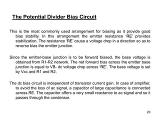
1
Chapter 3
TRANSITOR BIASING CIRCUITS AND
THERMAL STABILITY
2
Transistor Biasing
The basic function of transistor is amplification. The process of raising the
strength of weak signal without any change in its general shape is
referred as faithful amplification.
For faithful amplification it is essential that:-
1. Emitter-Base junction is forward biased
2. Collector- Base junction is reversed biased
3. Proper zero signal collector current
Transistor Biasing:
The proper flow of zero signal collector current and the
maintenance of proper collector emitter voltage during the
passage of signal is called transistor biasing.
3
4
WHY BIASING?
If the transistor is not biased properly, it would work inefficiently and
produce distortion in output signal.
HOW A TRANSISTOR CAN BE BIASED?
A transistor is biased either with the help of battery or associating a
circuit with the transistor. The later method is more efficient and is
frequently used. The circuit used for transistor biasing is called the
biasing circuit.
5
Bias Stability
The collector current in a transistor changes rapidly when
1) the temperature changes,
2) the transistor is replaced by another of the same type.
This is due to the inherent variations of transistor
parameters.
Through proper biasing, a desired quiescent operating point
of the transistor amplifier in the active region (linear region)
of the characteristics is obtained. It is desired that once
selected the operating point should remain stable. The
maintenance of operating point stable is called
Stabilisation.
6
Need for Stabilisation
The operating point of a transistor amplifier shifts mainly
with changes in temperature, since the transistor
parameters — β, ICO and VBE which are functions of
temperature.
Stabilisation of the operating point is necessary due to
the following reasons :
(i)Temperature dependence of IC
(ii)Individual variations
(iii)Thermal runaway
7
Stability Factor
Stability Factor S:- The rate of change of collector current IC w.r.t. the
collector leakage current *ICO at constant  and IB is called stability
factor
8
Stability Factor
9
Methods of Transistor Biasing
1) Base resistor method
2) Emitter bias method
3) Biasing with collector-feedback resistor
4) Voltage-divider bias
Base resistor method
10
Base resistor method
11
Base resistor method
12
Base resistor method
13
Advantages :
(i)This biasing circuit is very simple as only one resistance RB is
required.
(ii) Biasing conditions can easily be set, and the calculations are simple.
(iii) There is no loading of the source by the biasing circuit since no
resistor is employed across base-emitter junction.
Base resistor method
Disadvantages :
(i)This method provides poor stabilisation.
(ii)The stability factor is very high. Therefore, there are strong chances of thermal
runaway.
Due to these disadvantages, this method of biasing is rarely employed
14
15
The fixed bias circuit is modified
by attaching an external resistor
to the emitter. This resistor
introduces negative feedback
that stabilizes the Q-point.
Fixed bias with emitter resistor
16
Merits:
• The circuit has the tendency to stabilize operating point against changes in
temperature and β-value.
Demerits:
• As β-value is fixed for a given transistor, this relation can be satisfied either
by keeping RE very large, or making RB very low.
 If RE is of large value, high VCC is necessary. This increases cost
as well as precautions necessary while handling.
 If RB is low, a separate low voltage supply should be used in the base
circuit. Using two supplies of different voltages is impractical.
• In addition to the above, RE causes ac feedback which reduces the voltage
gain of the amplifier.
Usage:
The feedback also increases the input impedance of the amplifier when seen
from the base, which can be advantageous. Due to the above disadvantages,
this type of biasing circuit is used only with careful consideration of the trade-
offs involved.
17
The Collector to Base Bias Circuit
VCC
RC
C
E
B
RF
Ic
Ib
VBE
+
- IE
This configuration employs negative
feedback to prevent thermal runaway and
stabilize the operating point. In this form of
biasing, the base resistor RF is connected to
the collector instead of connecting it to the
DC source Vcc. So any thermal runaway will
induce a voltage drop across the Rc resistor
that will throttle the transistor's base current.
18
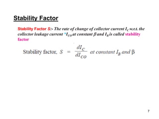
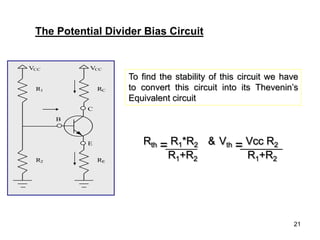
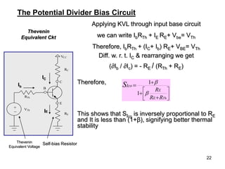
Applying KVL through base circuit
we can write (Ib+ IC) RC + Ib Rf+ Vbe= Vcc
Diff. w. r. t. IC we get
(∂Ib / ∂Ic) = - RC / (Rf + RC)
Therefore, SIco ═ (1+ β)
1+ [βRC/(RC+ Rf)]
Which is less than (1+β), signifying better thermal stability
19
Merits:
• Circuit stabilizes the operating point against variations in temperature
and β (i.e. replacement of transistor)
Demerits:
• As β -value is fixed (and generally unknown) for a given transistor, this
relation can be satisfied either by keeping Rc fairly large or making Rf very
low.
 If Rc is large, a high Vcc is necessary, which increases
cost as well as
precautions necessary while handling.
If Rf is low, the reverse bias of the collector–base region is
small, which limits the range of collector voltage swing that
leaves the transistor in active mode.
•The resistor Rf causes an AC feedback, reducing the voltage
gain of the amplifier. This undesirable effect is a trade-off for
greater Q-point stability.
Usage: The feedback also decreases the input impedance of the amplifier
as seen from the base, which can be advantageous. Due to the gain
reduction from feedback, this biasing form is used only when the trade-off
for stability is warranted.
20
This is the most commonly used arrangement for biasing as it provide good
bias stability. In this arrangement the emitter resistance ‘RE’ provides
stabilization. The resistance ‘RE’ cause a voltage drop in a direction so as to
reverse bias the emitter junction.
Since the emitter-base junction is to be forward biased, the base voltage is
obtained from R1-R2 network. The net forward bias across the emitter base
junction is equal to VB- dc voltage drop across ‘RE’. The base voltage is set
by Vcc and R1 and R2.
The dc bias circuit is independent of transistor current gain. In case of amplifier,
to avoid the loss of ac signal, a capacitor of large capacitance is connected
across RE. The capacitor offers a very small reactance to ac signal and so it
passes through the condensor.
The Potential Divider Bias Circuit
21
VCC
RC
C
E
B
VCC
R1
RE
R2
IE
IC
Ib
The Potential Divider Bias Circuit
To find the stability of this circuit we have
to convert this circuit into its Thevenin’s
Equivalent circuit
Rth = R1*R2 & Vth = Vcc R2
R1+R2 R1+R2
VCC
RC
C
E
B
VCC
R1
RE
R2
Rth = R1*R2 & Vth = Vcc R2
R1+R2 R1+R2
Rth = R1*R2 & Vth = Vcc R2
R1+R2 R1+R2
Rth = R1*R2 & Vth = Vcc R2
R1+R2 R1+R2
22
Applying KVL through input base circuit
we can write IbRTh + IE RE+ Vbe= VTh
Therefore, IbRTh + (IC+ Ib) RE+ VBE= VTh
Diff. w. r. t. IC & rearranging we get
(∂Ib / ∂Ic) = - RE / (RTh + RE)
Therefore,
This shows that SIco
is inversely proportional to RE
and It is less than (1+β), signifying better thermal
stability
Thevenin
Equivalent Ckt










Th
R
R
R
E
E
Ico
S


1
1
The Potential Divider Bias Circuit
VCC
RC
C
E
B
RE
RTh
VTh
_
+
Thevenin
Equivalent Voltage
Self-bias Resistor
IE
Ib
IC
23
Merits:
• Operating point is almost independent of β variation.
• Operating point stabilized against shift in temperature.
Demerits:
• As β-value is fixed for a given transistor, this relation can be satisfied either
by keeping RE fairly large, or making R1||R2 very low.
 If RE is of large value, high VCC is necessary. This increases cost as well
as precautions necessary while handling.
 If R1 || R2 is low, either R1 is low, or R2 is low, or both are low. A low R1
raises VB closer to VC, reducing the available swing in collector voltage,
and limiting how large RC can be made without driving the transistor out
of active mode. A low R2 lowers Vbe, reducing the allowed collector
current. Lowering both resistor values draws more current from the power
supply and lowers the input resistance of the amplifier as seen from the
base.
 AC as well as DC feedback is caused by RE, which reduces the AC
voltage gain of the amplifier. A method to avoid AC feedback while
retaining DC feedback is discussed below.
Usage:
The circuit's stability and merits as above make it widely used for linear
circuits.
24
Summary
• The Q-point is the best point for operation of a
transistor for a given collector current.
• The purpose of biasing is to establish a stable
operating point (Q-point).
• The linear region of a transistor is the region of
operation within saturation and cutoff.
• Out of all the biasing circuits, potential divider
bias circuit provides highest stability to operating
point.

Chapter 3 (2).ppt

  • 1.
    1 Chapter 3 TRANSITOR BIASINGCIRCUITS AND THERMAL STABILITY
  • 2.
    2 Transistor Biasing The basicfunction of transistor is amplification. The process of raising the strength of weak signal without any change in its general shape is referred as faithful amplification. For faithful amplification it is essential that:- 1. Emitter-Base junction is forward biased 2. Collector- Base junction is reversed biased 3. Proper zero signal collector current Transistor Biasing: The proper flow of zero signal collector current and the maintenance of proper collector emitter voltage during the passage of signal is called transistor biasing.
  • 3.
  • 4.
    4 WHY BIASING? If thetransistor is not biased properly, it would work inefficiently and produce distortion in output signal. HOW A TRANSISTOR CAN BE BIASED? A transistor is biased either with the help of battery or associating a circuit with the transistor. The later method is more efficient and is frequently used. The circuit used for transistor biasing is called the biasing circuit.
  • 5.
    5 Bias Stability The collectorcurrent in a transistor changes rapidly when 1) the temperature changes, 2) the transistor is replaced by another of the same type. This is due to the inherent variations of transistor parameters. Through proper biasing, a desired quiescent operating point of the transistor amplifier in the active region (linear region) of the characteristics is obtained. It is desired that once selected the operating point should remain stable. The maintenance of operating point stable is called Stabilisation.
  • 6.
    6 Need for Stabilisation Theoperating point of a transistor amplifier shifts mainly with changes in temperature, since the transistor parameters — β, ICO and VBE which are functions of temperature. Stabilisation of the operating point is necessary due to the following reasons : (i)Temperature dependence of IC (ii)Individual variations (iii)Thermal runaway
  • 7.
    7 Stability Factor Stability FactorS:- The rate of change of collector current IC w.r.t. the collector leakage current *ICO at constant  and IB is called stability factor
  • 8.
  • 9.
    9 Methods of TransistorBiasing 1) Base resistor method 2) Emitter bias method 3) Biasing with collector-feedback resistor 4) Voltage-divider bias
  • 10.
  • 11.
  • 12.
  • 13.
    Base resistor method 13 Advantages: (i)This biasing circuit is very simple as only one resistance RB is required. (ii) Biasing conditions can easily be set, and the calculations are simple. (iii) There is no loading of the source by the biasing circuit since no resistor is employed across base-emitter junction.
  • 14.
    Base resistor method Disadvantages: (i)This method provides poor stabilisation. (ii)The stability factor is very high. Therefore, there are strong chances of thermal runaway. Due to these disadvantages, this method of biasing is rarely employed 14
  • 15.
    15 The fixed biascircuit is modified by attaching an external resistor to the emitter. This resistor introduces negative feedback that stabilizes the Q-point. Fixed bias with emitter resistor
  • 16.
    16 Merits: • The circuithas the tendency to stabilize operating point against changes in temperature and β-value. Demerits: • As β-value is fixed for a given transistor, this relation can be satisfied either by keeping RE very large, or making RB very low.  If RE is of large value, high VCC is necessary. This increases cost as well as precautions necessary while handling.  If RB is low, a separate low voltage supply should be used in the base circuit. Using two supplies of different voltages is impractical. • In addition to the above, RE causes ac feedback which reduces the voltage gain of the amplifier. Usage: The feedback also increases the input impedance of the amplifier when seen from the base, which can be advantageous. Due to the above disadvantages, this type of biasing circuit is used only with careful consideration of the trade- offs involved.
  • 17.
    17 The Collector toBase Bias Circuit VCC RC C E B RF Ic Ib VBE + - IE This configuration employs negative feedback to prevent thermal runaway and stabilize the operating point. In this form of biasing, the base resistor RF is connected to the collector instead of connecting it to the DC source Vcc. So any thermal runaway will induce a voltage drop across the Rc resistor that will throttle the transistor's base current.
  • 18.
    18 Applying KVL throughbase circuit we can write (Ib+ IC) RC + Ib Rf+ Vbe= Vcc Diff. w. r. t. IC we get (∂Ib / ∂Ic) = - RC / (Rf + RC) Therefore, SIco ═ (1+ β) 1+ [βRC/(RC+ Rf)] Which is less than (1+β), signifying better thermal stability
  • 19.
    19 Merits: • Circuit stabilizesthe operating point against variations in temperature and β (i.e. replacement of transistor) Demerits: • As β -value is fixed (and generally unknown) for a given transistor, this relation can be satisfied either by keeping Rc fairly large or making Rf very low.  If Rc is large, a high Vcc is necessary, which increases cost as well as precautions necessary while handling. If Rf is low, the reverse bias of the collector–base region is small, which limits the range of collector voltage swing that leaves the transistor in active mode. •The resistor Rf causes an AC feedback, reducing the voltage gain of the amplifier. This undesirable effect is a trade-off for greater Q-point stability. Usage: The feedback also decreases the input impedance of the amplifier as seen from the base, which can be advantageous. Due to the gain reduction from feedback, this biasing form is used only when the trade-off for stability is warranted.
  • 20.
    20 This is themost commonly used arrangement for biasing as it provide good bias stability. In this arrangement the emitter resistance ‘RE’ provides stabilization. The resistance ‘RE’ cause a voltage drop in a direction so as to reverse bias the emitter junction. Since the emitter-base junction is to be forward biased, the base voltage is obtained from R1-R2 network. The net forward bias across the emitter base junction is equal to VB- dc voltage drop across ‘RE’. The base voltage is set by Vcc and R1 and R2. The dc bias circuit is independent of transistor current gain. In case of amplifier, to avoid the loss of ac signal, a capacitor of large capacitance is connected across RE. The capacitor offers a very small reactance to ac signal and so it passes through the condensor. The Potential Divider Bias Circuit
  • 21.
    21 VCC RC C E B VCC R1 RE R2 IE IC Ib The Potential DividerBias Circuit To find the stability of this circuit we have to convert this circuit into its Thevenin’s Equivalent circuit Rth = R1*R2 & Vth = Vcc R2 R1+R2 R1+R2 VCC RC C E B VCC R1 RE R2 Rth = R1*R2 & Vth = Vcc R2 R1+R2 R1+R2 Rth = R1*R2 & Vth = Vcc R2 R1+R2 R1+R2 Rth = R1*R2 & Vth = Vcc R2 R1+R2 R1+R2
  • 22.
    22 Applying KVL throughinput base circuit we can write IbRTh + IE RE+ Vbe= VTh Therefore, IbRTh + (IC+ Ib) RE+ VBE= VTh Diff. w. r. t. IC & rearranging we get (∂Ib / ∂Ic) = - RE / (RTh + RE) Therefore, This shows that SIco is inversely proportional to RE and It is less than (1+β), signifying better thermal stability Thevenin Equivalent Ckt           Th R R R E E Ico S   1 1 The Potential Divider Bias Circuit VCC RC C E B RE RTh VTh _ + Thevenin Equivalent Voltage Self-bias Resistor IE Ib IC
  • 23.
    23 Merits: • Operating pointis almost independent of β variation. • Operating point stabilized against shift in temperature. Demerits: • As β-value is fixed for a given transistor, this relation can be satisfied either by keeping RE fairly large, or making R1||R2 very low.  If RE is of large value, high VCC is necessary. This increases cost as well as precautions necessary while handling.  If R1 || R2 is low, either R1 is low, or R2 is low, or both are low. A low R1 raises VB closer to VC, reducing the available swing in collector voltage, and limiting how large RC can be made without driving the transistor out of active mode. A low R2 lowers Vbe, reducing the allowed collector current. Lowering both resistor values draws more current from the power supply and lowers the input resistance of the amplifier as seen from the base.  AC as well as DC feedback is caused by RE, which reduces the AC voltage gain of the amplifier. A method to avoid AC feedback while retaining DC feedback is discussed below. Usage: The circuit's stability and merits as above make it widely used for linear circuits.
  • 24.
    24 Summary • The Q-pointis the best point for operation of a transistor for a given collector current. • The purpose of biasing is to establish a stable operating point (Q-point). • The linear region of a transistor is the region of operation within saturation and cutoff. • Out of all the biasing circuits, potential divider bias circuit provides highest stability to operating point.