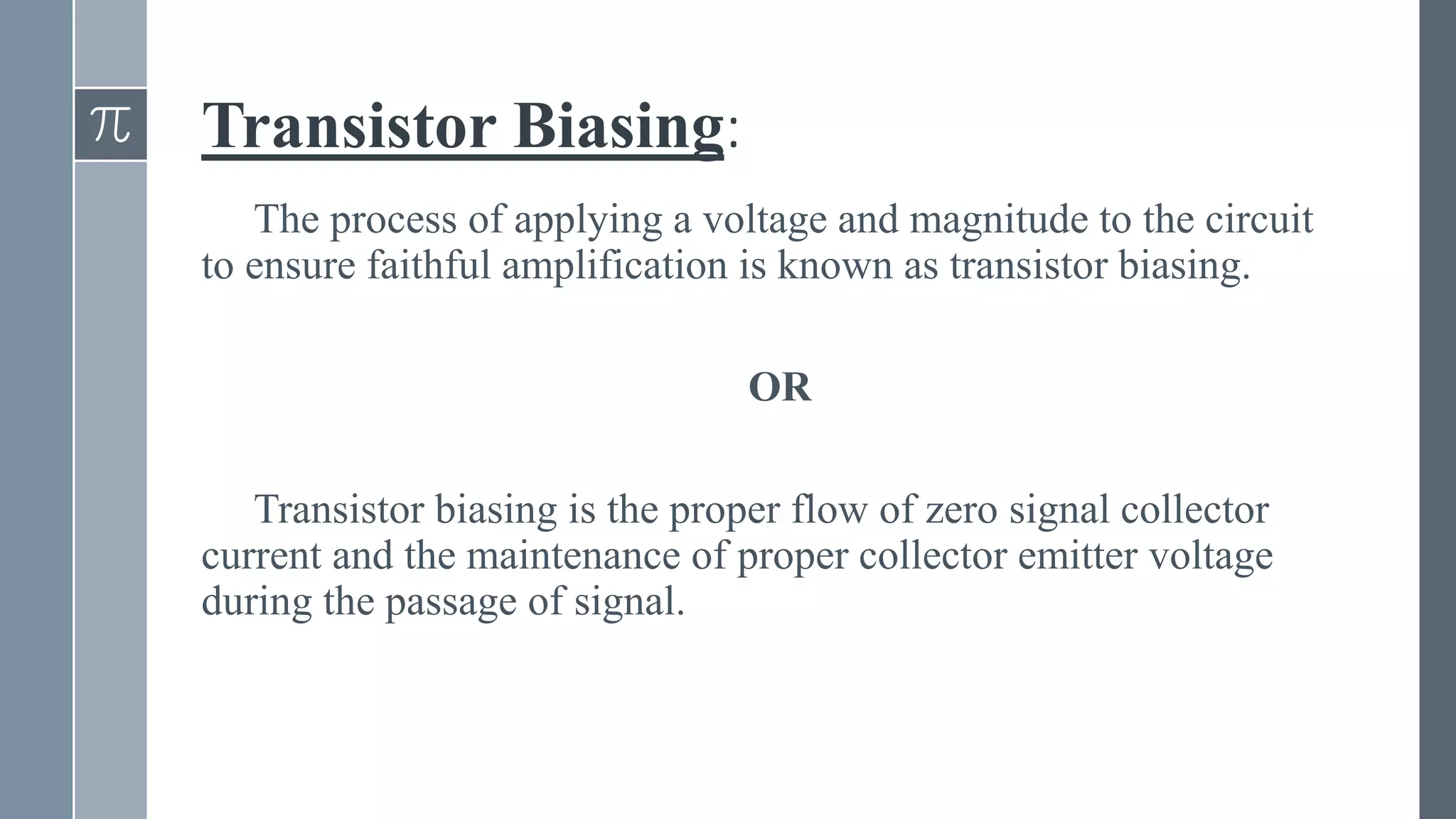
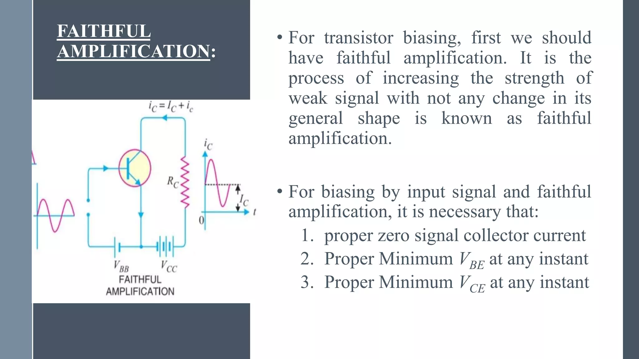
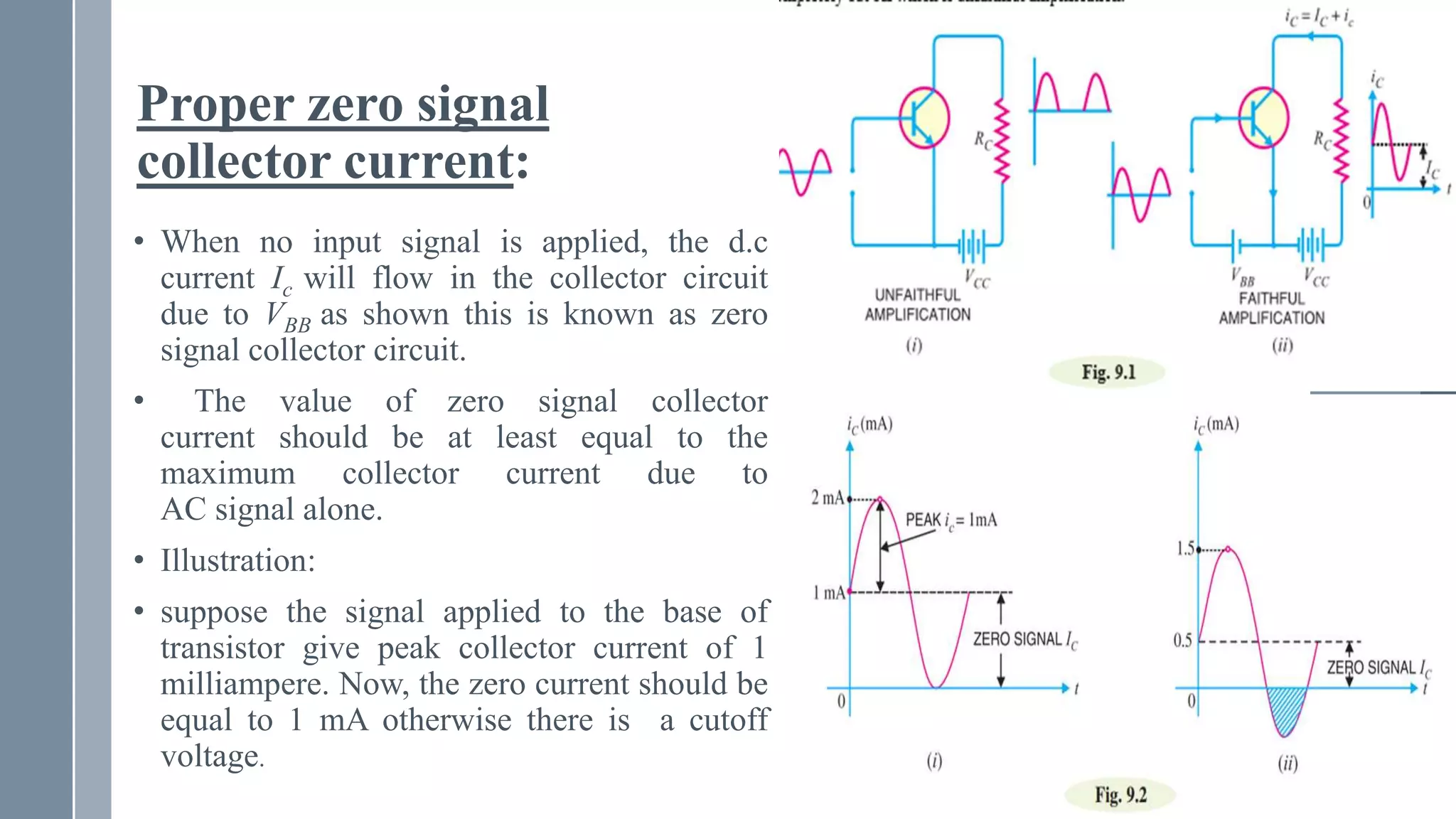
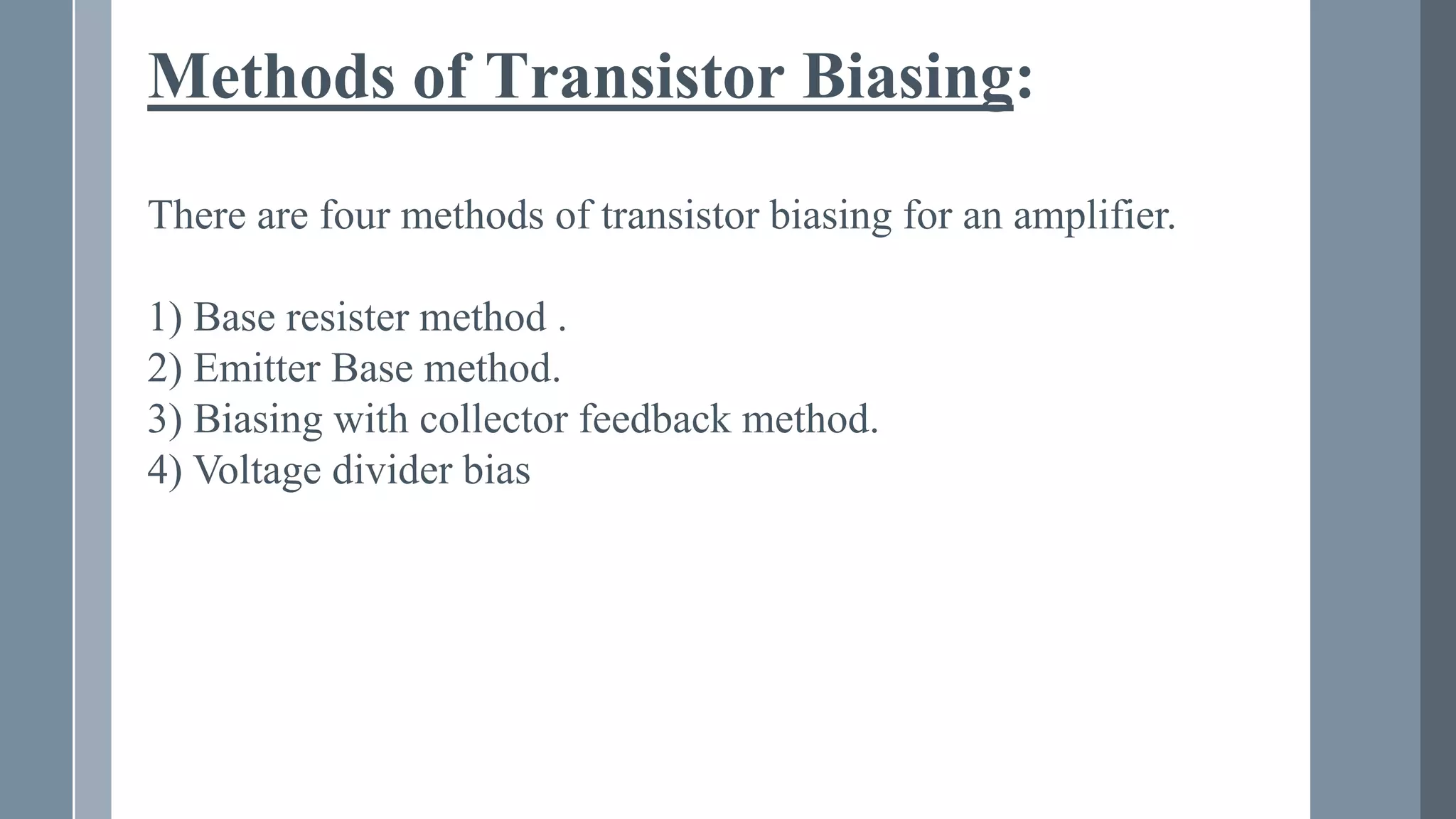
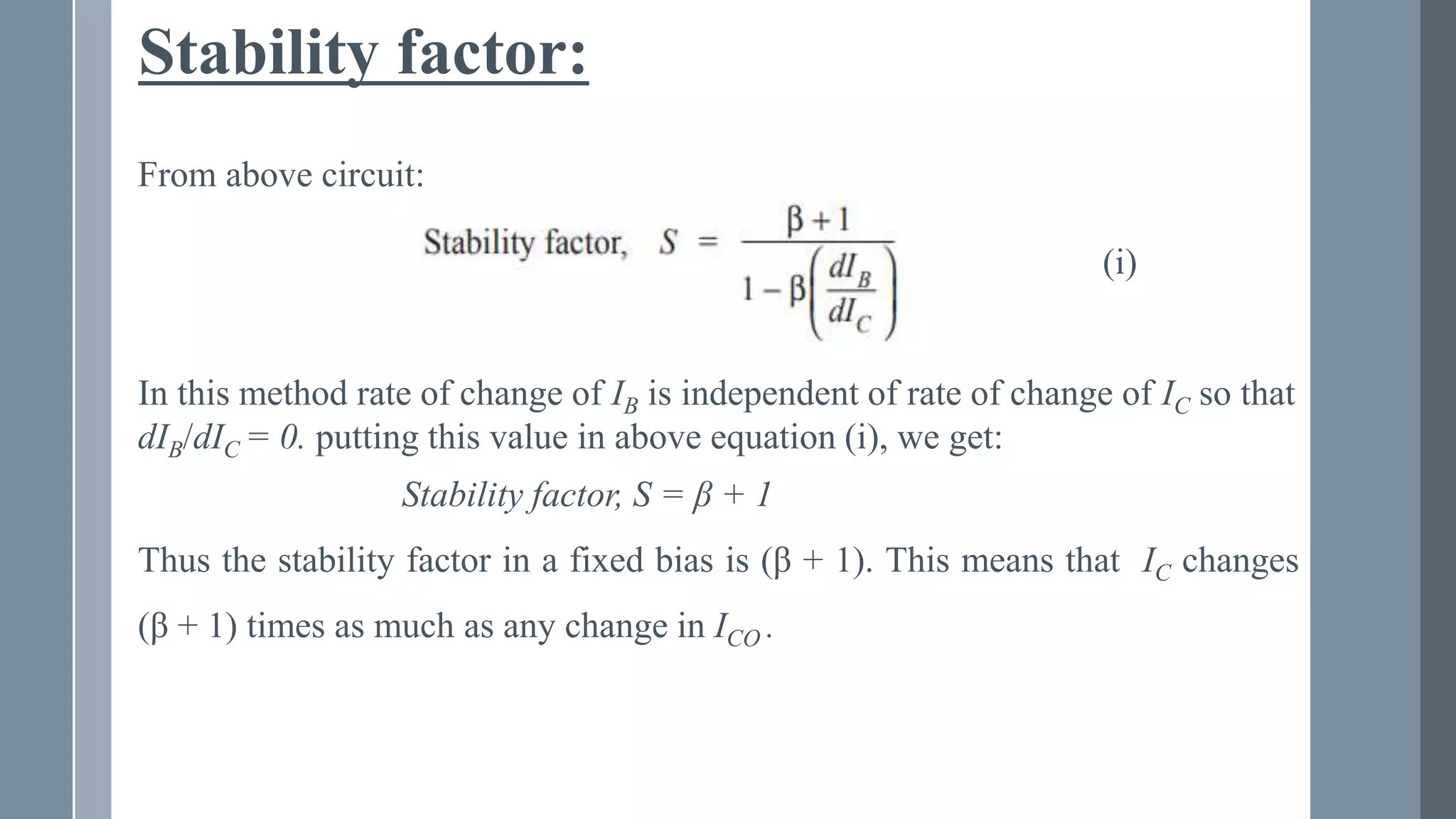
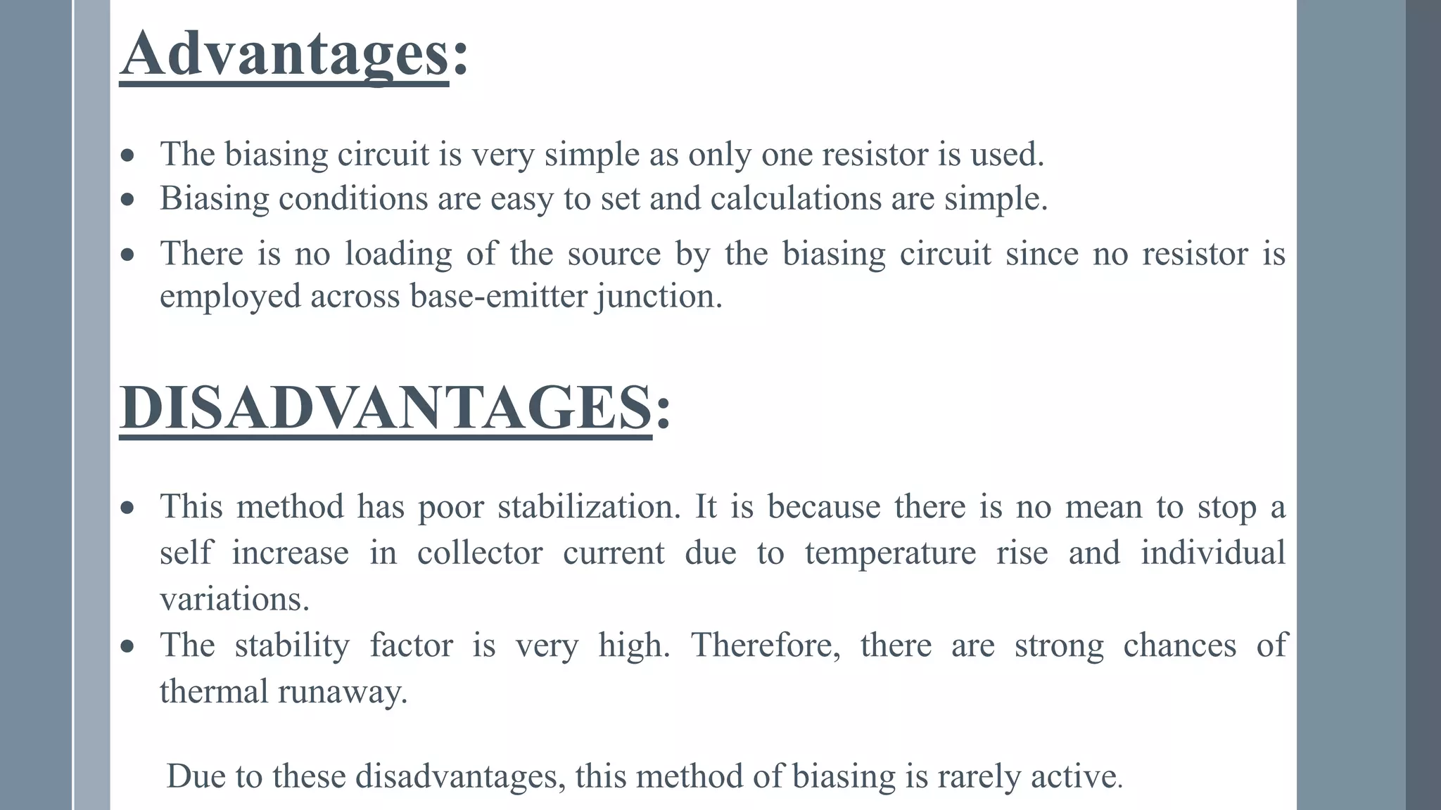
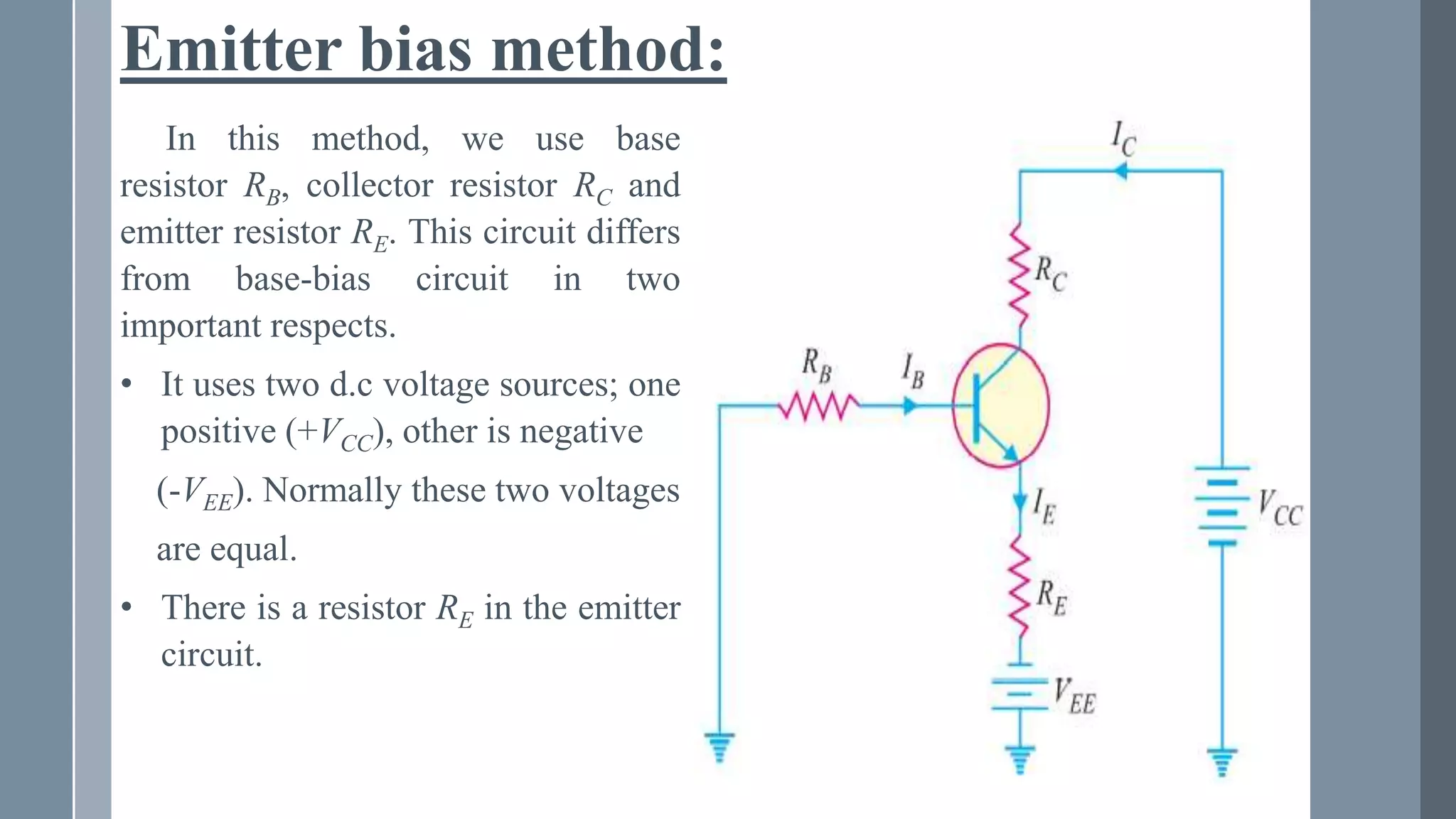
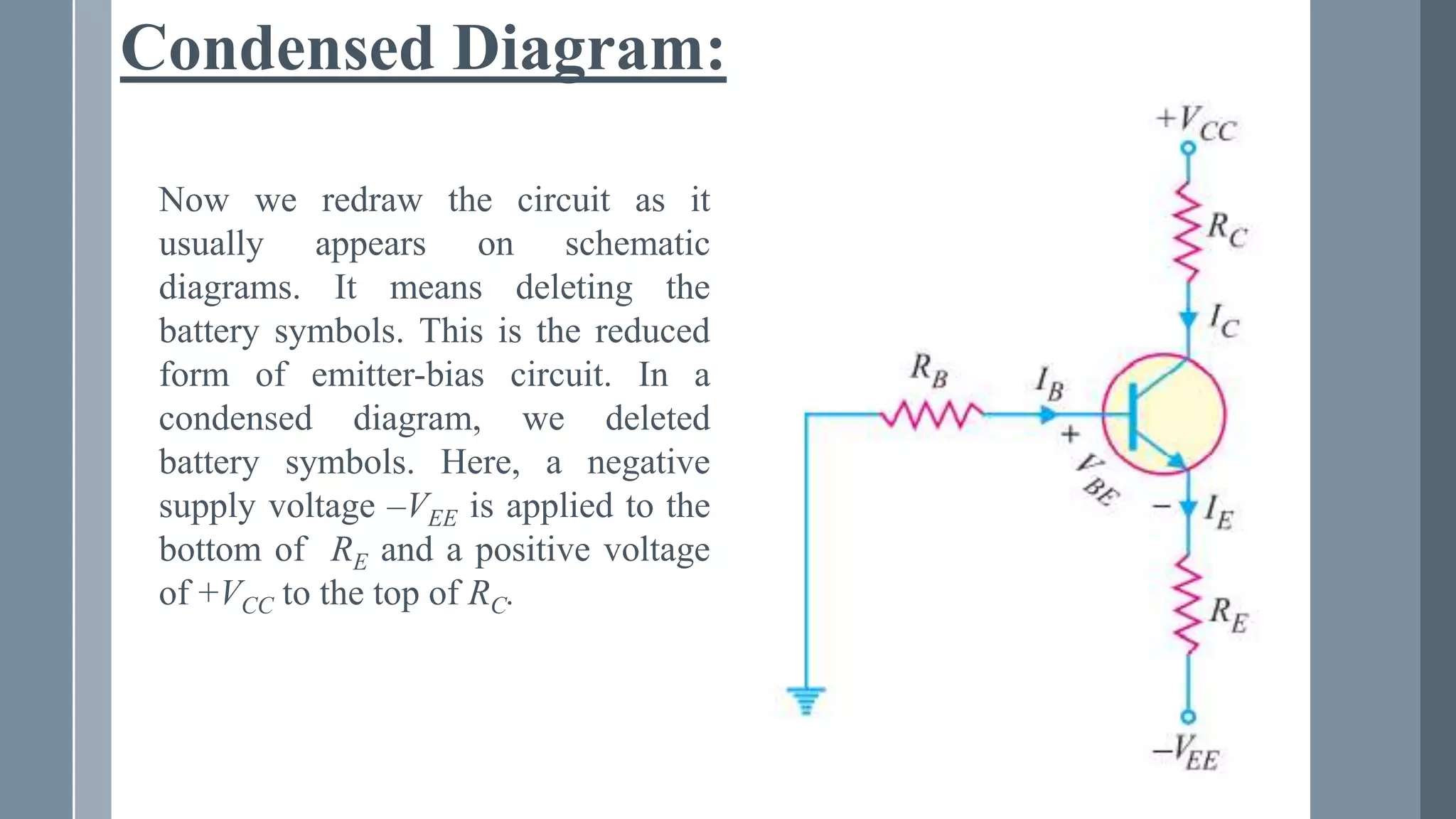
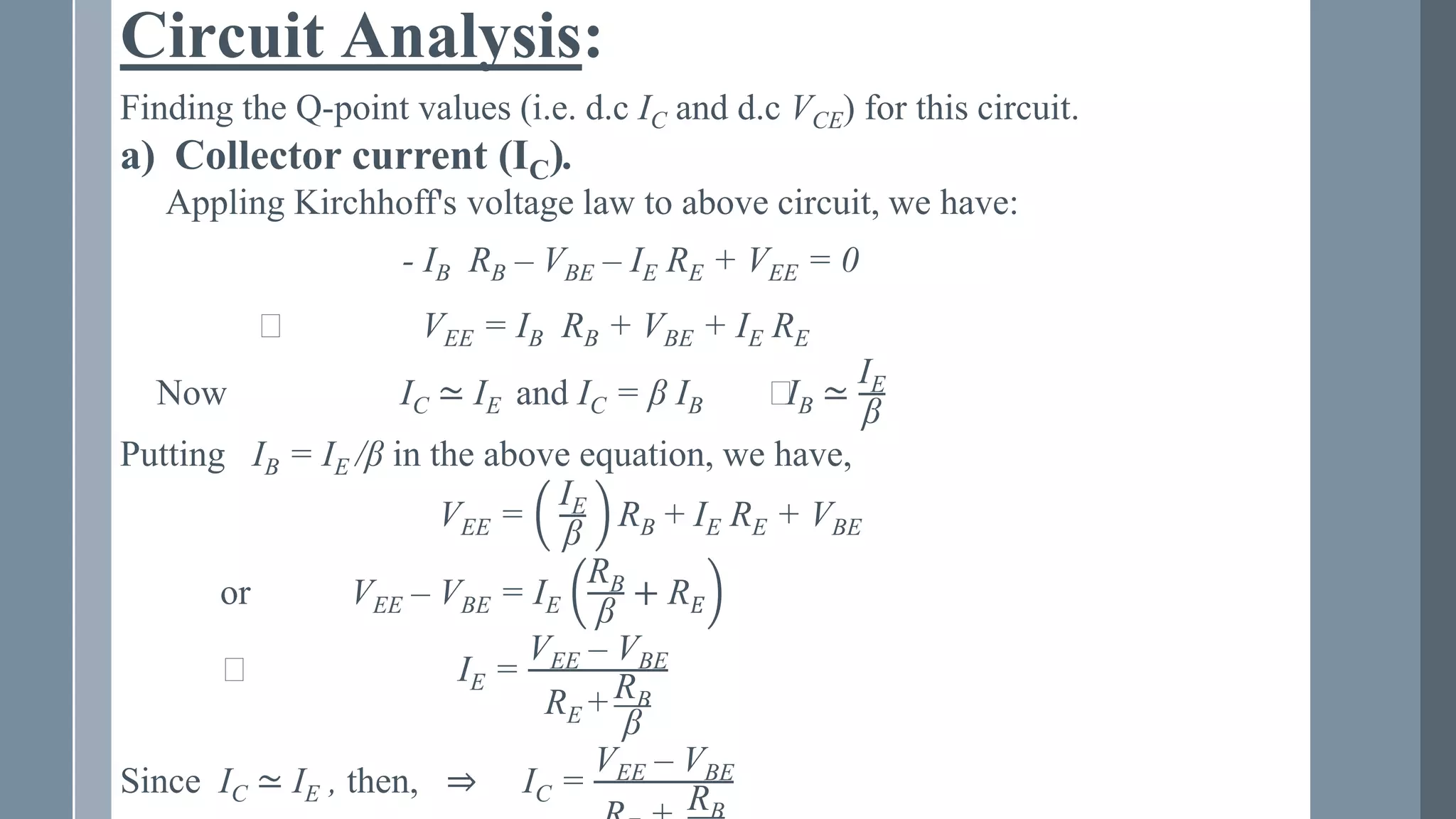
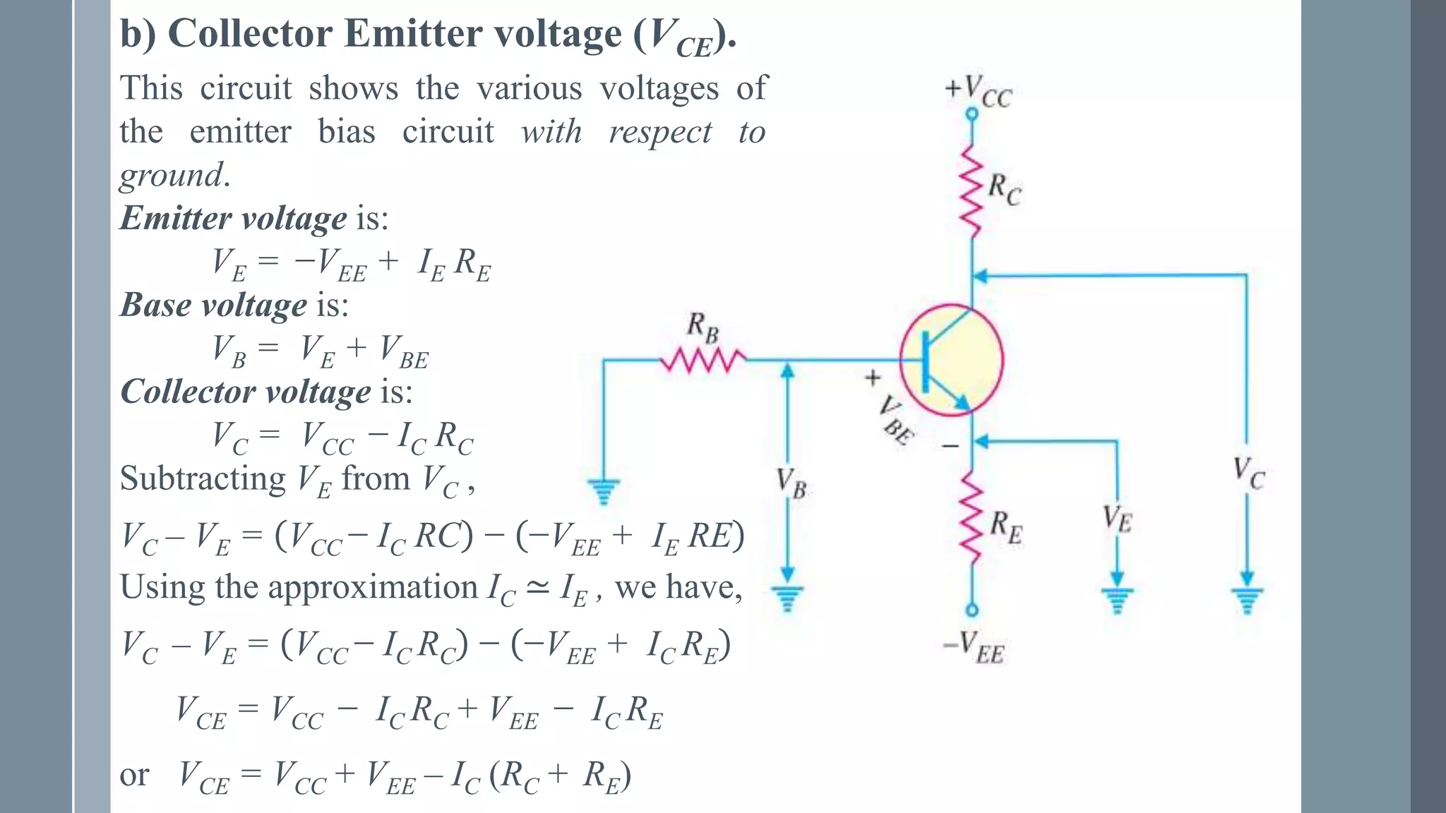
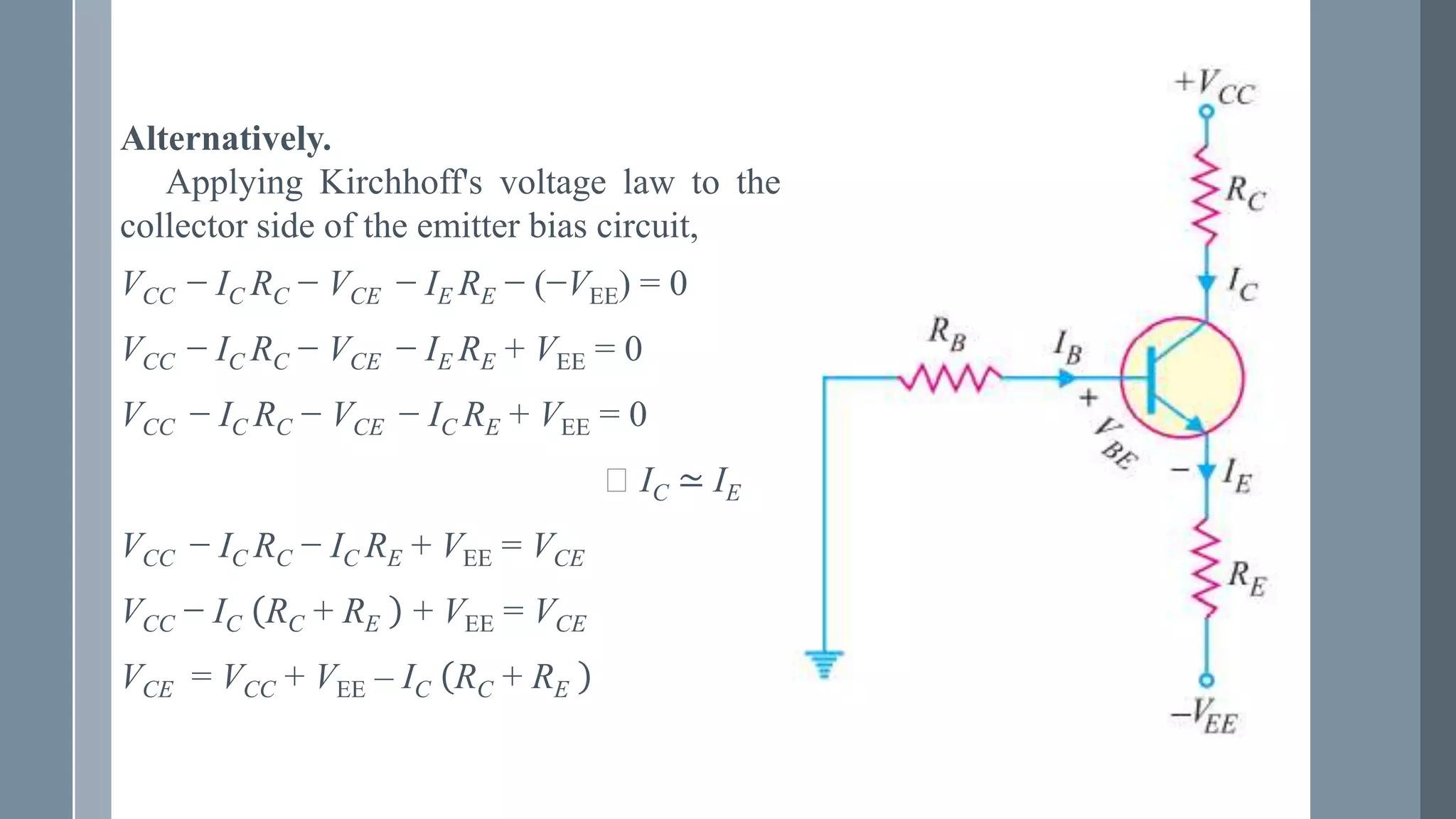
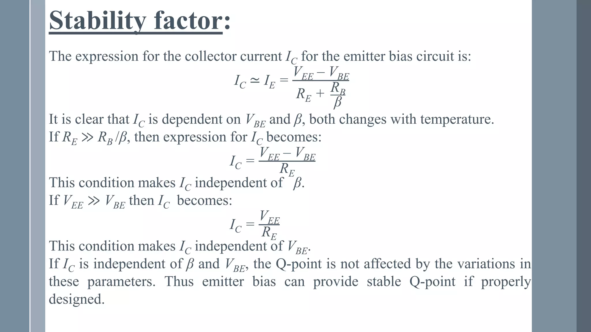
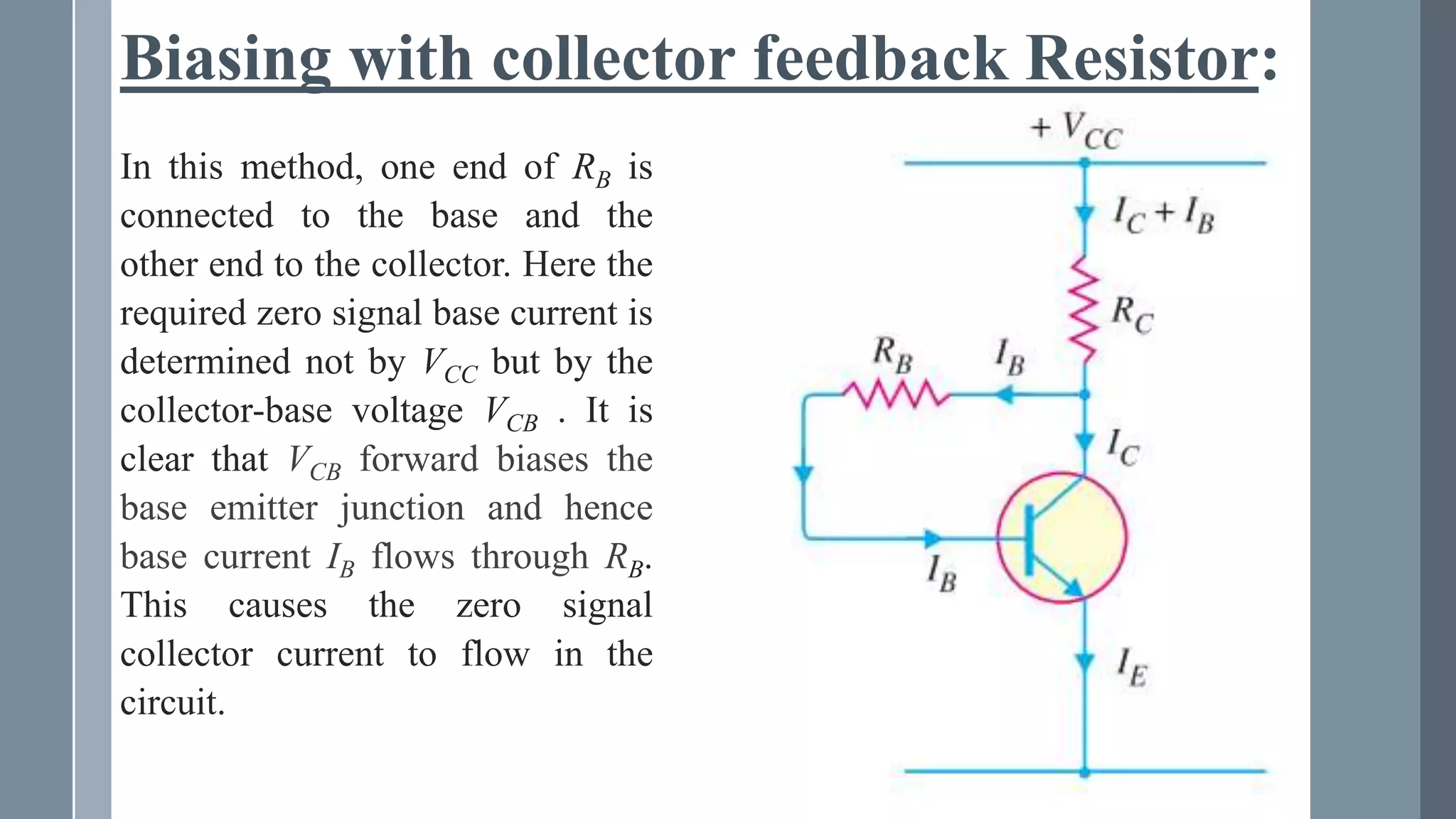
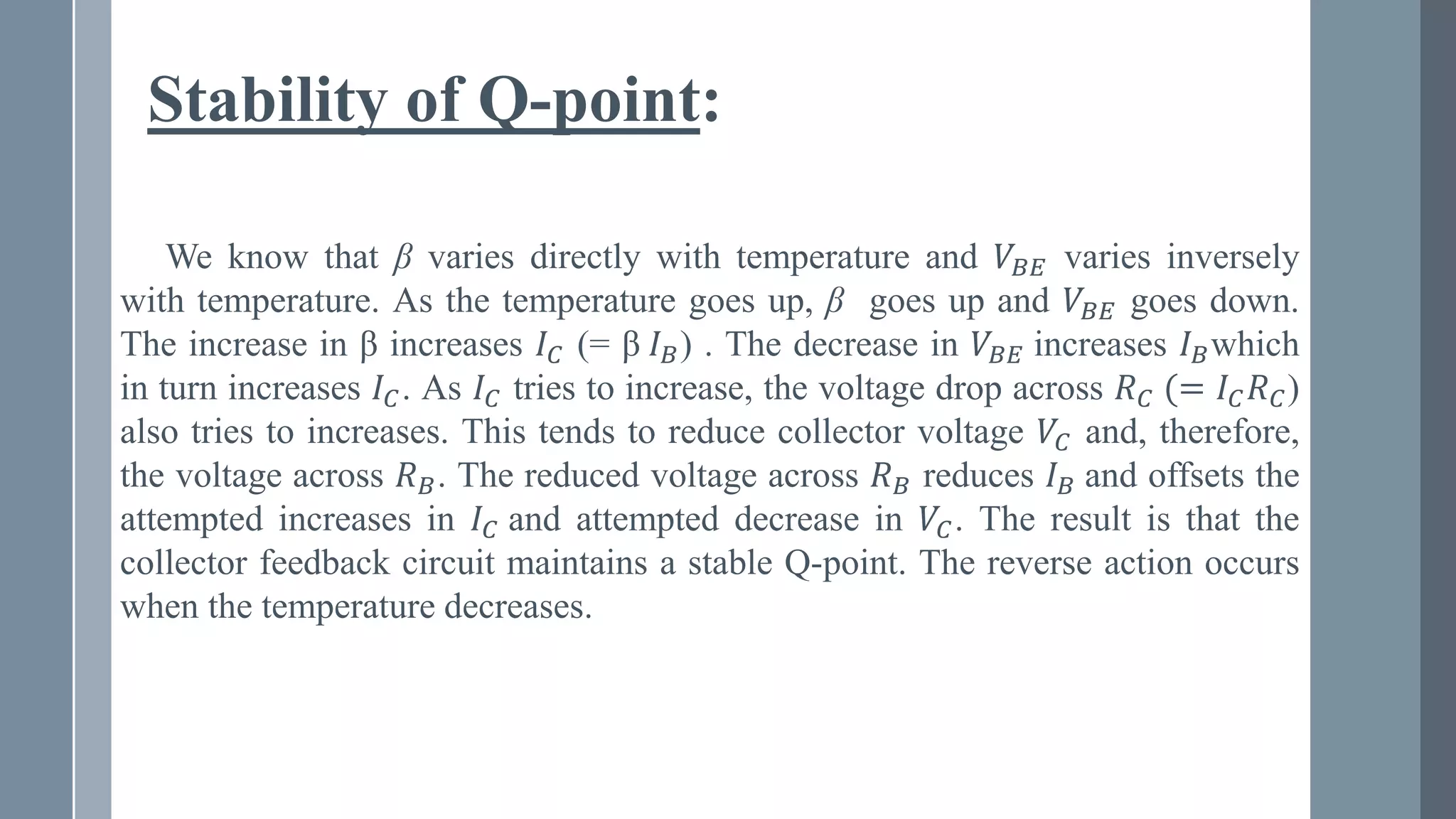
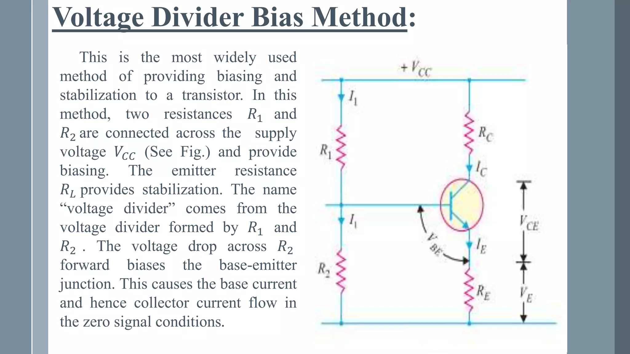
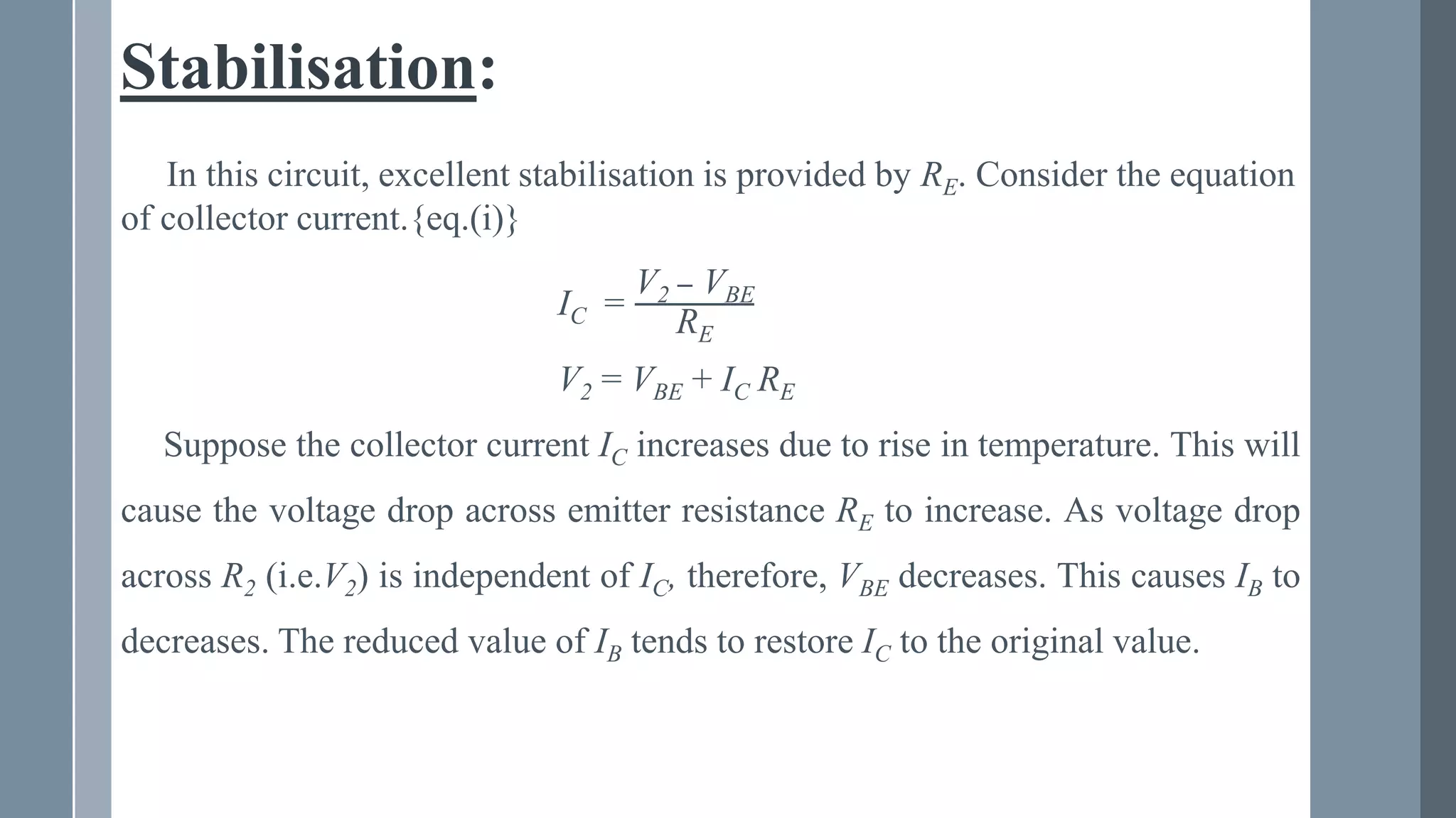
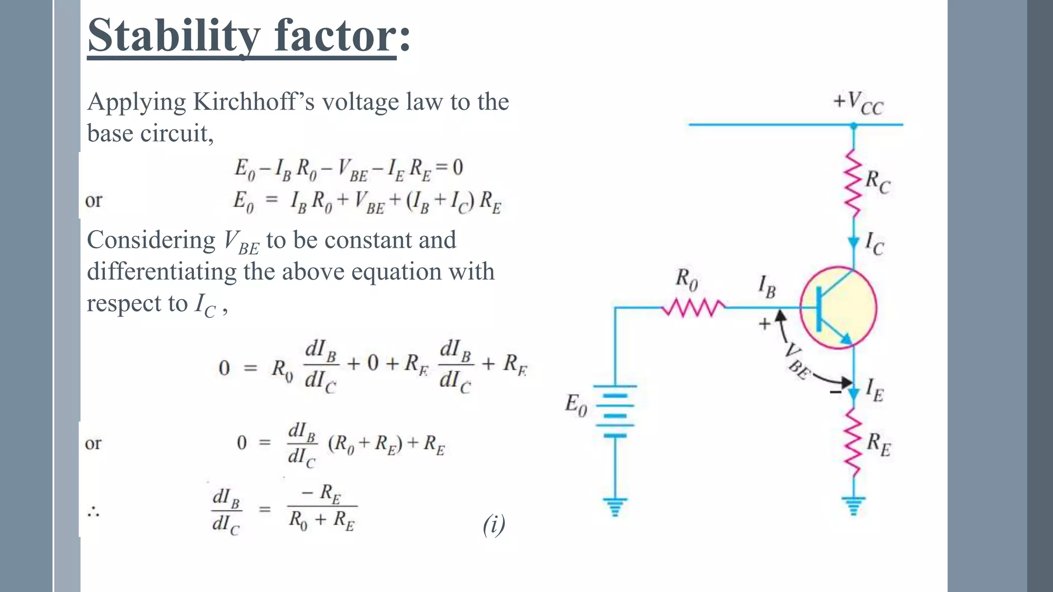
discussing differences faithful and un- faithful amplification
discussing stabilition in transistors
and how temperature affect collector current
discussing various methods of transistor biasing like
Base resister method ,Emitter Base method , Biasing with collector feedback method , Voltage divider bias
Transistors can be used as switches or amplifiers. The document discusses the basics of bipolar transistors including their structure, operation, and different configurations (common base, common emitter, common collector). It provides examples of calculating currents and voltages in transistor circuits using characteristics curves and explains how different classes of amplifiers (A, B, AB, C) determine the portion of the input signal cycle during which the transistor is active.
1. The document discusses the principles of operation of p-n junction diodes and their use in analog electronic circuits. It describes how a diode only conducts current in one direction when forward biased and acts as an open switch when reverse biased.
2. Diode clipper circuits are introduced which can clip off portions of an input signal by only allowing the signal to pass through the diode when above or below a certain threshold set by a bias voltage. Parallel and series clipper configurations are examined along with their input-output characteristics.
3. Double-ended clipper circuits are described which can clip both the positive and negative portions of a signal simultaneously using two back-to-back diodes biased to conduct only
This document discusses transistor bias circuits. It explains that a transistor must be properly biased with a DC voltage in order to operate as a linear amplifier. A voltage divider bias circuit is then introduced as a practical method for establishing the DC operating point. The voltage divider uses two resistors connected from the positive supply to ground to set the base voltage. As long as the base current is small compared to the divider current, the base voltage will remain relatively constant. Graphs of transistor characteristics are also used to illustrate how the operating point is established on the load line between cutoff and saturation.
This document discusses different biasing schemes for BJTs, including fixed bias, collector base bias, and voltage divider bias. It explains how each biasing scheme works, its advantages and disadvantages, typical applications, and how stability is achieved. The key points are:
1) Different biasing schemes like fixed bias, collector base bias and voltage divider bias are used to set the operating point of BJTs and provide stability against variations in temperature, transistor parameters etc.
2) Collector base bias provides better stability than fixed bias by using negative feedback, but it reduces gain. Voltage divider bias is most widely used as it provides both stable biasing and high gain.
3) Stability is improved by
BJT Biasing for B.Tech Ist Year EngineeringRaghav Bansal
Okay, let's solve this step-by-step:
1) Given: IC = 2 mA
2) We're told IC = βIB
3) So we can set up and solve for β:
IC = βIB
2 mA = βIB
β = IC/IB = 2 mA / 0.5 mA = 4
So the answer for part a is:
β = 4
4) We're also given: IB = 0.5 mA
5) Using the voltage divider formula:
VB = VCC * (RB2 / (RB1 + RB2))
6) We know: VB = 0.7 V (for the B-
This document contains lecture slides about BJT transistors and amplifier circuits. It discusses BJT biasing, modes of operation, input and output characteristics, and analysis of transistor circuits using voltage loops. Examples are provided to demonstrate analyzing DC operating points and determining AC quantities like transconductance and input resistance. The document also introduces small-signal models for analyzing transistor amplifiers.
- The document discusses the structure and operation of bipolar junction transistors (BJTs), specifically NPN and PNP transistors.
- It describes the basic BJT components - emitter, base, and collector - and how current flows when the emitter-base junction is forward biased and the collector-base junction is reverse biased, known as the active mode.
- Key points covered include how the base current is a fraction of the collector current, represented by the current gain β, and how the emitter current can be expressed in terms of the collector and base currents.
- Equivalent circuit models of the BJT are presented, including the common emitter configuration with β as the current gain.
1) CE amplifiers use bias circuits to set an operating point for the transistor. Simple bias circuits vary with transistor parameters like beta.
2) Load line analysis graphs the interplay between circuit constraints and the transistor output characteristic to determine the operating point.
3) Stabilized bias circuits aim to fix the emitter current independently of beta using an emitter resistor and potential divider bias network. Negative feedback bias circuits also use feedback from the collector voltage.
Common emitter amplifier by YEASIN NEWAJYeasinNewaj
This slide has been created for students who are studying electrical engineering and who want to gain knowledge of basic electronics. The topic is COMMON EMITTER AMPLIFIER OF BJT
The document discusses bipolar junction transistors (BJTs). It covers:
1) The basic structure of a BJT, which consists of three doped semiconductor regions forming two back-to-back PN junctions.
2) The common NPN and PNP transistor configurations and their symbols. BJTs operate by forward biasing one PN junction and reverse biasing the other.
3) Key characteristics including current gain (beta) and the different regions of operation - cutoff, active, and saturation. BJTs are commonly used as linear amplifiers and switches.
This document discusses bipolar junction transistors (BJTs). It describes the basic structure and operation of NPN and PNP BJTs, including their three terminals (base, emitter, collector), current flow, and biasing. BJTs can be used as switches in digital circuits or amplifiers in analog circuits. The document also covers BJT characteristics such as active, saturation, and cutoff regions; DC current gains; and voltage relationships. BJT amplifier classes like Class A, B, AB, and C are introduced along with their relative efficiencies. Stabilization techniques for BJT amplifiers using emitter feedback and voltage divider biasing are also summarized.
The document discusses bipolar junction transistors (BJTs). It describes the basic construction of an NPN and PNP transistor including the emitter, base, and collector regions. It explains that the base-emitter junction must be forward biased and the base-collector junction must be reverse biased for the transistor to operate properly. The document also discusses BJT biasing circuits, operating regions including cutoff, saturation, and active modes, and uses of BJTs as switches and amplifiers.
Bipolar junction transistor : Biasing and AC AnalysisTahmina Zebin
1. The document discusses various transistor amplifier circuit designs and analysis techniques, including biasing circuits like base bias, voltage divider bias, and emitter feedback bias.
2. It introduces the small-signal h-parameter transistor model that represents the transistor under AC conditions and defines terms like small-signal current gain and output conductance.
3. The document provides examples of calculating Q-points, load lines, and biasing component values for different transistor amplifier circuits.
The document provides information about bipolar junction transistors (BJTs), including:
1) BJTs have three doped semiconductor regions (emitter, base, collector) separated by two pn junctions and operate using both holes and electrons.
2) For a BJT to operate as an amplifier, the base-emitter junction must be forward-biased and the base-collector junction must be reverse-biased.
3) Changes in base current cause much larger changes in collector current, allowing BJTs to amplify signals.
A bipolar junction transistor (BJT) has three regions - the emitter, base, and collector - separated by two pn junctions. In normal operation, the base-emitter junction is forward-biased and the base-collector junction is reverse-biased. The current flowing into the base controls the much larger currents flowing between the collector and emitter. BJTs can be used as amplifiers, switches, or other circuit elements depending on the biasing conditions. Key specifications include the current gain and maximum voltage and current ratings.
The document discusses bipolar junction transistors (BJTs) and their operation. It begins by introducing the npn and pnp transistor structures, which contain three doped regions: emitter, base, and collector. It describes the active, cutoff, and saturation regions of operation. The document then provides mathematical expressions to relate the emitter, base, and collector currents based on the common-emitter configuration. It also discusses the common-base current gain and common-emitter current gain. Examples are provided to calculate different transistor parameters like beta, alpha, and currents. Finally, the common-emitter configuration and its current-voltage characteristics are summarized.
This document provides an overview of bipolar junction transistors (BJT) including:
- The basic structure of an NPN or PNP transistor with emitter, base, and collector layers.
- How transistors operate in cutoff, saturation, and active modes depending on biasing of the PN junctions.
- How a small base current controls a larger collector current in the active region, allowing transistors to function as electronic switches or amplifiers.
The document summarizes some basic characteristics of transistors:
1. The forward current transfer ratio (CB) is represented by a horizontal line on an Ic-VCB graph, showing Ic=IE. The DC current gain (α) is defined as the ratio of collector current (Ic) to base current (IE).
2. The AC current gain (β) is the ratio of changes in collector and base currents. It is typically less than 1, but the transistor still provides voltage and power gain due to the high load resistance.
3. The relation between α and β is defined as β=α/(1-α) and α=β/(1-β).
Bipolar junction transistors (BJTs) are composed of three sections of semiconductors with different dopings. The middle section is the base, which is narrow. BJTs come in NPN and PNP variants. NPN transistors are more common as electrons move faster. A BJT acts as a valve, controlling current flow between the collector and emitter terminals based on the base current. To analyze BJT circuits, one must determine if the transistor is in cutoff, active-linear, or saturation mode by checking voltages and currents against the transistor's characteristics.
This document provides information about the diac, including its structure, operation, and applications. It discusses how a diac is a bidirectional semiconductor device that can be switched from an OFF state to an ON state with either polarity of applied voltage. When the applied voltage exceeds the breakover voltage, the diac begins conducting. Diacs are commonly used to trigger triacs in applications like light dimmers and heat controls to smoothly vary the output voltage through phase control of AC power.
DC biasing applies fixed voltages to transistors to place them in an operating region for amplification. The operating point defines the transistor's quiescent operating conditions under DC. Stability refers to a circuit's insensitivity to parameter variations like temperature. Emitter-stabilized and voltage divider biasing improve stability over fixed biasing by incorporating an emitter or voltage divider resistor. Feedback biasing further increases stability by introducing negative feedback from collector to base.
The document discusses the AC analysis of BJT and MOSFET inverting amplifiers. It begins by stating the lesson objectives which are to draw small signal models, calculate parameters, and analyze performance characteristics like voltage gain, input and output resistances. It then discusses the hybrid-pi model of BJTs and defines the transconductance, output resistance and input resistance. Equivalent circuit models are shown for common-emitter and common-source amplifiers using BJTs and MOSFETs. Calculations are presented for voltage gain, input and output resistances of these amplifiers both with and without bypassing the emitter or source resistances. Examples are also worked through.
The document discusses the bipolar junction transistor (BJT) including its physical structure and operation, current-voltage characteristics in common-base, common-emitter, and saturation modes, use in amplifier circuits, and biasing techniques. It covers topics such as equivalent circuit models, transconductance, input and output resistances, and the design of common-emitter amplifiers. Diagrams illustrate equivalent circuits, amplifier bias points, and the graphical analysis of amplifier behavior.
Through proper biasing, a desired quiescent operating point of the transistor amplifier in the active region (linear region) of the characteristics is obtained. It is desired that once selected the operating point should remain stable. The maintenance of operating point stable is called Stabilisation.
transistor biasing and
stability factor , β
The document describes a voltage divider bias circuit for a BJT transistor that provides stability using a single voltage supply. It contains a link to a lab manual on building the circuit, lists related BJT experiments, and explains that running a DC analysis will obtain the collector current, base current, base voltage, emitter voltage, and collector voltage values.
Emitter bias method of transistor biasingAnisur Rahman
Transistor biasing is the process of setting a transistor's operating voltage or current levels so that an AC input signal can be correctly amplified. There are several commonly used biasing methods including emitter biasing. Emitter biasing uses both positive and negative power supplies to provide a stable bias that fluctuates little with temperature variation or transistor replacement. It works by using the voltage drop across an emitter resistor from the emitter current to forward bias the emitter-base junction. Any increase in emitter current further reverse biases the junction, keeping the bias stable. Resistor values are typically chosen such that the emitter resistor voltage drop is 10% of the power supply voltage and the base resistor current
Rec101 unit ii (part 2) bjt biasing and re modelDr Naim R Kidwai
This document discusses biasing of bipolar junction transistors (BJTs) including different biasing configurations such as fixed bias, emitter bias, voltage divider bias, and collector feedback. It explains how setting the operating or quiescent point on the transistor characteristics curve is important for proper amplification. The concepts of cutoff, saturation and active regions are covered. Equations for analyzing common emitter, common base and common collector configurations are provided. An example calculation of the collector current and voltage at the operating point is shown. Finally, bias stability and factors affecting it are briefly discussed.
This document discusses transistor biasing and faithful signal amplification in transistors. It begins by explaining that the basic function of a transistor is amplification, and that for faithful amplification the input circuit must remain forward biased and the output circuit must remain reverse biased during the signal. This is achieved through transistor biasing, which provides the proper zero-signal collector current, base-emitter voltage, and collector-emitter voltage. Several common biasing circuits are described, including base resistor, collector feedback resistor, and voltage divider methods. The key requirements for faithful amplification and the effects of improper biasing are illustrated. Transistor characteristics like the input curve and output curve are also discussed.
Transistors are semiconductor devices with three terminals - collector, base, and emitter. There are two main types, NPN and PNP, which differ in the doping of the semiconductor regions. Bipolar transistors can operate as amplifiers, switches, or oscillators depending on the biasing conditions. The common emitter configuration provides voltage gain but inverts the phase, while common base and common collector configurations do not invert phase. Transistor gain is determined by factors like current gain (beta) and varies based on operating point and temperature.
This document summarizes key aspects of the bipolar junction transistor (BJT). It describes the BJT as a three-layer semiconductor device with two p-n junctions: the emitter-base junction and the collector-base junction. The emitter-base junction is forward biased for amplification while the collector-base junction is reverse biased. There are three main configurations for connecting a BJT in a circuit: common emitter, common base, and common collector. The document provides details on the input and output characteristics of each configuration. It also compares the properties of the configurations in terms of factors like voltage gain, current gain, and input/output resistances.
This document discusses transistor biasing circuits. It outlines different types of biasing circuits including fixed bias, emitter bias, collector feedback bias, and voltage divider bias. It explains how each circuit works, analyzing key parameters like collector current, collector-emitter voltage, and stability factor. The goal of biasing circuits is to set the transistor's operating point in the active region for faithful signal amplification while stabilizing it against temperature and other variations. Voltage divider bias is highlighted as the most widely used method due to its ability to stabilize the operating point through negative feedback.
1) Bipolar junction transistors (BJTs) are commonly used semiconductor devices that can be used as amplifiers and logic switches. They consist of three terminals: collector, base, and emitter.
2) There are several types of biasing circuits that can be used with BJTs, including fixed bias, collector feedback bias, fixed bias with emitter resistor, and voltage divider biasing. Biasing circuits ensure that the BJT operates in its active region.
3) The characteristics curves of different biasing circuits show how voltages and currents vary with each other. Mathematical equations can be derived to describe the relationships between voltages and currents for different biasing configurations.
There are four main methods of transistor biasing: base resistor method, emitter bias method, biasing with collector feedback resistor, and voltage-divider bias method. The document then focuses on explaining the base resistor method and voltage-divider bias method in more detail. For the base resistor method, a resistor is used to provide base current, but it has poor stability. For the voltage-divider bias method, two resistors are used to provide stable biasing of the transistor by controlling the base-emitter voltage. This method is widely used due to its stability from the emitter resistor preventing changes in collector current.
Biasing is the process of applying external voltages to transistors to ensure proper operation. It involves forward or reverse biasing transistor junctions to place the device in specific regions like active, saturation, or cutoff. Common biasing circuits include fixed bias using a base resistor, collector-to-base bias which provides feedback, and emitter bias where a resistor is added to stabilize operating point. Proper biasing establishes a quiescent point and load line on the transistor characteristics curve for linear amplification.
DC Biasing – Bipolar Junction Transistors (BJTs)ssuserb29892
This document discusses various methods of biasing bipolar junction transistors (BJTs) for proper operation, including voltage-divider bias, emitter bias, and collector feedback bias. It explains that transistors must be biased to establish a stable operating point between cutoff and saturation. Various bias circuits are analyzed using Kirchhoff's laws and the transistor model. Key aspects of establishing bias, such as determining the quiescent point and load lines, as well as sources of instability and techniques to improve stability, are covered. Examples are provided to illustrate calculating important bias parameters.
This document discusses biasing circuits for BJTs. It begins by explaining that biasing circuits apply DC voltages to establish fixed operating points for transistors. This allows them to operate in the linear region. It then discusses several common biasing circuits: fixed bias, emitter-stabilized bias, and voltage divider bias. The fixed bias circuit uses two resistors and provides DC paths. The emitter-stabilized bias adds a resistor at the emitter for improved stability. The voltage divider bias uses a voltage divider network to provide DC voltages, making the operating point largely independent of transistor beta. It analyzes examples of each circuit type and discusses how to determine key voltages and currents like the Q-point, VCE, and
Common Emitter Configuration and Collector CurveZeeshan Rafiq
This document discusses common emitter configuration in transistors. It describes:
- The common emitter configuration has the emitter common to both input and output terminals. It provides high gain and is widely used in amplifier designs.
- The input characteristics are similar to a diode with the output characteristics relating collector current (IC) to collector voltage (VCE) for different base currents (IB).
- The active, cutoff, and saturation regions are described on the output characteristics graph.
Electrical current, voltage, resistance, capacitance, and inductance are a few of the basic elements of electronics and radio. Apart from current, voltage, resistance, capacitance, and inductance, there are many other interesting elements to electronic technology. ... Use Electronics Notes to learn electronics online.
The document discusses transistor biasing and stabilization. It defines biasing as establishing a quiescent point (Q-point) for the transistor in the active region through supply voltages and resistances. This allows distortion-free amplification. Thermal runaway occurs when increased collector current further increases junction temperature, leading to uncontrollable positive feedback. Several biasing circuits are described, including fixed bias, emitter feedback bias, collector-to-base feedback bias, collector-emitter feedback bias, and voltage divider/emitter bias. Stability factor is a measure of how sensitive the collector current is to changes in the transistor's reverse saturation current. Voltage divider bias establishes a Q-point independently of beta through a resistor
The potential divider bias circuit provides the most stable operating point (Q-point) for a transistor. It uses two resistors (R1 and R2) in a potential divider configuration to set the base voltage, and a third resistor (RE) connected from the emitter to ground introduces negative feedback. This feedback makes the Q-point nearly independent of temperature variations and transistor parameter changes, providing the highest stability of any biasing circuit.
Transistor biasing circuits establish a quiescent operating point (Q-point) for the transistor in the active region to produce distortion-free amplification. Five common biasing circuits are described: fixed bias, emitter feedback bias, collector feedback bias, collector-emitter feedback bias, and self/emitter bias. The self/emitter bias circuit forms a voltage divider with external resistors to set the base voltage independently of beta, improving stability against temperature variations and beta changes between transistors. Stability is quantified by the stability factor and improved by increasing the emitter resistor relative to the base resistor.
This document discusses biasing schemes and stability of BJT transistors. It describes four common biasing schemes - fixed bias, collector base bias, voltage divider bias, and emitter bias. Voltage divider bias is the most widely used as it provides both biasing and stabilization. Stabilization is important to prevent thermal runaway from temperature and parameter variations. The stability factor S indicates how sensitive the collector current is to changes in the collector-base leakage current. Lower S provides better stability.
Bipolar junction transistor characterstics biassing and amplification, lab 9kehali Haileselassie
This document summarizes an experiment on characterizing the input and output properties of a bipolar junction transistor (BJT) and demonstrating its signal amplification capabilities. The experiment involved establishing the transistor's DC operating point, then evaluating its small-signal AC operation. Key results included measuring the transistor's DC current gain and small-signal voltage gain, which compared reasonably well to theoretical predictions. The document also discussed the different regions of BJT operation and their implications for circuit applications.
Bipolar junction transistor characterstics biassing and amplification, lab 9kehali Haileselassie
This document summarizes an experiment on characterizing the input and output properties of a bipolar junction transistor (BJT) and demonstrating its ability to amplify signals when biased in the active region. Key findings include:
1) Measured voltages and currents matched predicted values closely, both from hand calculations and PSPICE simulations.
2) In the active region, a small AC input signal produced a larger AC output signal, demonstrating amplification. Measured gains matched predictions from an equivalent circuit model.
3) BJT regions of interest - active, cutoff, and saturation - were explored. In the active region the BJT acts as a current source, enabling its use as a signal amplifier.
Transistor cb cc ce power point transistor2004akkuu
This document discusses transistor configurations and biasing. It describes the common base, common emitter, and common collector configurations. It explains how biasing circuits like fixed bias, collector feedback bias, and voltage divider bias can stabilize the operating point. Thermal runaway and the use of heat sinks are also covered. Single-stage amplifiers using common emitter configuration with input and output coupling capacitors are discussed. Finally, the concepts of frequency response and bandwidth are introduced.
Similar to Electronics and modern physics presentation (20)
Nucleophilic Addition of carbonyl compounds.pptxSSR02
Nucleophilic addition is the most important reaction of carbonyls. Not just aldehydes and ketones, but also carboxylic acid derivatives in general.
Carbonyls undergo addition reactions with a large range of nucleophiles.
Comparing the relative basicity of the nucleophile and the product is extremely helpful in determining how reversible the addition reaction is. Reactions with Grignards and hydrides are irreversible. Reactions with weak bases like halides and carboxylates generally don’t happen.
Electronic effects (inductive effects, electron donation) have a large impact on reactivity.
Large groups adjacent to the carbonyl will slow the rate of reaction.
Neutral nucleophiles can also add to carbonyls, although their additions are generally slower and more reversible. Acid catalysis is sometimes employed to increase the rate of addition.
ANAMOLOUS SECONDARY GROWTH IN DICOT ROOTS.pptxRASHMI M G
Abnormal or anomalous secondary growth in plants. It defines secondary growth as an increase in plant girth due to vascular cambium or cork cambium. Anomalous secondary growth does not follow the normal pattern of a single vascular cambium producing xylem internally and phloem externally.
Current Ms word generated power point presentation covers major details about the micronuclei test. It's significance and assays to conduct it. It is used to detect the micronuclei formation inside the cells of nearly every multicellular organism. It's formation takes place during chromosomal sepration at metaphase.
hematic appreciation test is a psychological assessment tool used to measure an individual's appreciation and understanding of specific themes or topics. This test helps to evaluate an individual's ability to connect different ideas and concepts within a given theme, as well as their overall comprehension and interpretation skills. The results of the test can provide valuable insights into an individual's cognitive abilities, creativity, and critical thinking skills
Deep Behavioral Phenotyping in Systems Neuroscience for Functional Atlasing a...Ana Luísa Pinho
Functional Magnetic Resonance Imaging (fMRI) provides means to characterize brain activations in response to behavior. However, cognitive neuroscience has been limited to group-level effects referring to the performance of specific tasks. To obtain the functional profile of elementary cognitive mechanisms, the combination of brain responses to many tasks is required. Yet, to date, both structural atlases and parcellation-based activations do not fully account for cognitive function and still present several limitations. Further, they do not adapt overall to individual characteristics. In this talk, I will give an account of deep-behavioral phenotyping strategies, namely data-driven methods in large task-fMRI datasets, to optimize functional brain-data collection and improve inference of effects-of-interest related to mental processes. Key to this approach is the employment of fast multi-functional paradigms rich on features that can be well parametrized and, consequently, facilitate the creation of psycho-physiological constructs to be modelled with imaging data. Particular emphasis will be given to music stimuli when studying high-order cognitive mechanisms, due to their ecological nature and quality to enable complex behavior compounded by discrete entities. I will also discuss how deep-behavioral phenotyping and individualized models applied to neuroimaging data can better account for the subject-specific organization of domain-general cognitive systems in the human brain. Finally, the accumulation of functional brain signatures brings the possibility to clarify relationships among tasks and create a univocal link between brain systems and mental functions through: (1) the development of ontologies proposing an organization of cognitive processes; and (2) brain-network taxonomies describing functional specialization. To this end, tools to improve commensurability in cognitive science are necessary, such as public repositories, ontology-based platforms and automated meta-analysis tools. I will thus discuss some brain-atlasing resources currently under development, and their applicability in cognitive as well as clinical neuroscience.
Phenomics assisted breeding in crop improvementIshaGoswami9
As the population is increasing and will reach about 9 billion upto 2050. Also due to climate change, it is difficult to meet the food requirement of such a large population. Facing the challenges presented by resource shortages, climate
change, and increasing global population, crop yield and quality need to be improved in a sustainable way over the coming decades. Genetic improvement by breeding is the best way to increase crop productivity. With the rapid progression of functional
genomics, an increasing number of crop genomes have been sequenced and dozens of genes influencing key agronomic traits have been identified. However, current genome sequence information has not been adequately exploited for understanding
the complex characteristics of multiple gene, owing to a lack of crop phenotypic data. Efficient, automatic, and accurate technologies and platforms that can capture phenotypic data that can
be linked to genomics information for crop improvement at all growth stages have become as important as genotyping. Thus,
high-throughput phenotyping has become the major bottleneck restricting crop breeding. Plant phenomics has been defined as the high-throughput, accurate acquisition and analysis of multi-dimensional phenotypes
during crop growing stages at the organism level, including the cell, tissue, organ, individual plant, plot, and field levels. With the rapid development of novel sensors, imaging technology,
and analysis methods, numerous infrastructure platforms have been developed for phenotyping.
ESR spectroscopy in liquid food and beverages.pptxPRIYANKA PATEL
With increasing population, people need to rely on packaged food stuffs. Packaging of food materials requires the preservation of food. There are various methods for the treatment of food to preserve them and irradiation treatment of food is one of them. It is the most common and the most harmless method for the food preservation as it does not alter the necessary micronutrients of food materials. Although irradiated food doesn’t cause any harm to the human health but still the quality assessment of food is required to provide consumers with necessary information about the food. ESR spectroscopy is the most sophisticated way to investigate the quality of the food and the free radicals induced during the processing of the food. ESR spin trapping technique is useful for the detection of highly unstable radicals in the food. The antioxidant capability of liquid food and beverages in mainly performed by spin trapping technique.
The debris of the ‘last major merger’ is dynamically youngSérgio Sacani
The Milky Way’s (MW) inner stellar halo contains an [Fe/H]-rich component with highly eccentric orbits, often referred to as the
‘last major merger.’ Hypotheses for the origin of this component include Gaia-Sausage/Enceladus (GSE), where the progenitor
collided with the MW proto-disc 8–11 Gyr ago, and the Virgo Radial Merger (VRM), where the progenitor collided with the
MW disc within the last 3 Gyr. These two scenarios make different predictions about observable structure in local phase space,
because the morphology of debris depends on how long it has had to phase mix. The recently identified phase-space folds in Gaia
DR3 have positive caustic velocities, making them fundamentally different than the phase-mixed chevrons found in simulations
at late times. Roughly 20 per cent of the stars in the prograde local stellar halo are associated with the observed caustics. Based
on a simple phase-mixing model, the observed number of caustics are consistent with a merger that occurred 1–2 Gyr ago.
We also compare the observed phase-space distribution to FIRE-2 Latte simulations of GSE-like mergers, using a quantitative
measurement of phase mixing (2D causticality). The observed local phase-space distribution best matches the simulated data
1–2 Gyr after collision, and certainly not later than 3 Gyr. This is further evidence that the progenitor of the ‘last major merger’
did not collide with the MW proto-disc at early times, as is thought for the GSE, but instead collided with the MW disc within
the last few Gyr, consistent with the body of work surrounding the VRM.
Remote Sensing and Computational, Evolutionary, Supercomputing, and Intellige...University of Maribor
Slides from talk:
Aleš Zamuda: Remote Sensing and Computational, Evolutionary, Supercomputing, and Intelligent Systems.
11th International Conference on Electrical, Electronics and Computer Engineering (IcETRAN), Niš, 3-6 June 2024
Inter-Society Networking Panel GRSS/MTT-S/CIS Panel Session: Promoting Connection and Cooperation
https://www.etran.rs/2024/en/home-english/
What is greenhouse gasses and how many gasses are there to affect the Earth.moosaasad1975
What are greenhouse gasses how they affect the earth and its environment what is the future of the environment and earth how the weather and the climate effects.
Or: Beyond linear.
Abstract: Equivariant neural networks are neural networks that incorporate symmetries. The nonlinear activation functions in these networks result in interesting nonlinear equivariant maps between simple representations, and motivate the key player of this talk: piecewise linear representation theory.
Disclaimer: No one is perfect, so please mind that there might be mistakes and typos.
dtubbenhauer@gmail.com
Corrected slides: dtubbenhauer.com/talks.html
2. Transistor Biasing:
The process of applying a voltage and magnitude to the circuit
to ensure faithful amplification is known as transistor biasing.
OR
Transistor biasing is the proper flow of zero signal collector
current and the maintenance of proper collector emitter voltage
during the passage of signal.
3. FAITHFUL
AMPLIFICATION:
• For transistor biasing, first we should
have faithful amplification. It is the
process of increasing the strength of
weak signal with not any change in its
general shape is known as faithful
amplification.
• For biasing by input signal and faithful
amplification, it is necessary that:
1. proper zero signal collector current
2. Proper Minimum VBE at any instant
3. Proper Minimum VCE at any instant
4. Proper zero signal
collector current:
• When no input signal is applied, the d.c
current Ic will flow in the collector circuit
due to VBB as shown this is known as zero
signal collector circuit.
• The value of zero signal collector
current should be at least equal to the
maximum collector current due to
AC signal alone.
• Illustration:
• suppose the signal applied to the base of
transistor give peak collector current of 1
milliampere. Now, the zero current should be
equal to 1 mA otherwise there is a cutoff
voltage.
5. Proper Minimum VBE:
• In order to achieve faithful amplification, VBE should not fall below 0.5 V for
germanium and 0.7 V for silicon transistors. The base current is very small until
the input voltage overcomes the potential barrier at the base-emitter junction.
Once the potential barrier is overcome, the base current and hence collector
current increases sharply. But below potential barrier, the output is not properly
biased, and results in unfaithful amplification.
• Therefore, if base-emitter voltage VBE falls below these values during any part of
the signal, that part will be amplified to lesser extent due to small collector
current. This will result in unfaithful amplification.
6. Proper
Minimum VCE:
• For faithful amplification,
the collector-emitter
voltage VCE should not fall
below 0.5V for Ge
transistors and 1V for
silicon transistors. This is
called knee voltage.
Otherwise, it is forward
biased and instead of
attracting VCE it repel VCE.
• The value of VCE should
not be less than input
signal, otherwise it is not
amplified.
7. Stabilization:
The collector current IC in a transistor changes rapidly when
a) Temperature changes
b) Transistor is replaced by another of the same type. This is due to the
inherent variations (𝛽 − 𝑣𝑎𝑙𝑢𝑒) of transistor parameters.
When the temperature changes or the transistor is replaced, the operating
point also changes. However for faithful amplification, it is essential that
operating point remains fixed. This needs to make the operating point
independent of these variations. This is known as stabilization.
“The process of making operating point (zero signal IC and VBE)
independent of temperature changes and variations in transistor parameters is
called stabilization”.
Need for stabilization:
Stabilization of the operating point is necessary due to the following reasons:
(i) Individual variations (iii) Thermal runaway
(ii) Temperature dependence of IC
8. Temperature dependence of IC:
• The collector leakage current ICBO is greatly influenced (especially in
germanium transistor) by temperature changes. A rise of 10°C doubles
the collector leakage current ICBO which may be as high as 0.2 mA for
low powered germanium transistors. So, it also increases the IC.
IC = β IB + (β + 1) ICBO
Thermal runaway:
The self-destruction of unstabilised transistor is called thermal runaway.
The flow of IC produces heat in the transistor , which increases
temperature ,and it increases ICBO and it will increase the IC again. And
this process repeat again, and in few minutes , increase in IC will burn the
transistor.
To avoid thermal runaway, we decrease IB with temperature and IB
compensate the leakage current and it makes IC constant.
9. Stability factor:
The rate of change of collector current IC with respect to the
collector leakage current ICO at constant β and IB is called Stability
factor.
S = d IC / d ICO
IC =β IB + (β + 1) ICO
1 = β d IB / d Ic + (β + 1) d ICO / d Ic
1 = β d IB / d Ic + (β + 1) / S ⸪ 1/S = d ICO/ d Ic
S =
𝛽+1
1−𝛽
ⅆ𝐼𝑏
ⅆ𝐼𝑐
10. There are four methods of transistor biasing for an amplifier.
1) Base resister method .
2) Emitter Base method.
3) Biasing with collector feedback method.
4) Voltage divider bias
Methods of Transistor Biasing:
11. Base resistor method:
In this method, a high resistance RB
(several hundred kilo ohm) is connected
between the base and positive end of
supply for npn transistor. For pnp
transistor, RB is connected between the
base and negative end of supply. Here,
required zero signal base current is
provided by VCC and it flows through RB
. The base is positive w.r.t emitter. Base
emitter junction is forward biased. We
use the value of RB to get the value of
zero signal base current.
IC = β IB
12. Circuit Analysis:
To find RB , Collector current flows in the zero signal condition is required: Let
IC is a required zero signal collector current. Consider ABENA a closed circuit.
Now we apply Kirchhoff's voltage law,
VCC = IB RB + VBE
or IB RB = VCC – VBE
⸫ RB =
VCC – VBE
IB
VBE is very small as compared to VCC , then we neglect it:
RB =
VCC
IB
VCC is a known quantity and IB is chosen at some suitable value. Here, RB can
calculate directly and for this reason this method is sometimes called fixed
biased method.
13. Stability factor:
From above circuit:
(i)
In this method rate of change of IB is independent of rate of change of IC so that
dIB/dIC = 0. putting this value in above equation (i), we get:
Stability factor, S = β + 1
Thus the stability factor in a fixed bias is (β + 1). This means that IC changes
(β + 1) times as much as any change in ICO .
14. Advantages:
The biasing circuit is very simple as only one resistor is used.
Biasing conditions are easy to set and calculations are simple.
There is no loading of the source by the biasing circuit since no resistor is
employed across base-emitter junction.
DISADVANTAGES:
This method has poor stabilization. It is because there is no mean to stop a
self increase in collector current due to temperature rise and individual
variations.
The stability factor is very high. Therefore, there are strong chances of
thermal runaway.
Due to these disadvantages, this method of biasing is rarely active.
15. Emitter bias method:
In this method, we use base
resistor RB, collector resistor RC and
emitter resistor RE. This circuit differs
from base-bias circuit in two
important respects.
• It uses two d.c voltage sources; one
positive (+VCC), other is negative
(-VEE). Normally these two voltages
are equal.
• There is a resistor RE in the emitter
circuit.
16. Condensed Diagram:
Now we redraw the circuit as it
usually appears on schematic
diagrams. It means deleting the
battery symbols. This is the reduced
form of emitter-bias circuit. In a
condensed diagram, we deleted
battery symbols. Here, a negative
supply voltage –VEE is applied to the
bottom of RE and a positive voltage
of +VCC to the top of RC.
17. Circuit Analysis:
Finding the Q-point values (i.e. d.c IC and d.c VCE) for this circuit.
a) Collector current (IC).
Appling Kirchhoff's voltage law to above circuit, we have:
- IB RB – VBE – IE RE + VEE = 0
⸫ VEE = IB RB + VBE + IE RE
Now IC ≃ IE and IC = β IB ⸫
IB ≃
IE
β
Putting IB = IE /β in the above equation, we have,
VEE =
IE
β
RB + IE RE + VBE
or VEE – VBE = IE
RB
β
+ R𝐸
⸫ IE =
VEE – VBE
RE + RB
β
Since IC ≃ IE , then, ⇒ IC =
VEE – VBE
RB
18. b) Collector Emitter voltage (VCE).
This circuit shows the various voltages of
the emitter bias circuit with respect to
ground.
Emitter voltage is:
VE = −VEE + IE RE
Base voltage is:
VB = VE + VBE
Collector voltage is:
VC = VCC − IC RC
Subtracting VE from VC ,
VC – VE = VCC − IC RC − −VEE + IE RE
Using the approximation IC ≃ IE , we have,
VC – VE = VCC − IC RC − −VEE + IC RE
VCE = VCC − IC RC + VEE − IC RE
or VCE = VCC + VEE – IC (RC + RE)
19. Alternatively.
Applying Kirchhoff's voltage law to the
collector side of the emitter bias circuit,
VCC − IC RC − VCE − IE RE − (−VEE) = 0
VCC − IC RC − VCE − IE RE + VEE = 0
VCC − IC RC − VCE − IC RE + VEE = 0
⸪ IC ≃ IE
VCC − IC RC − IC RE + VEE = VCE
VCC − IC RC + RE + VEE = VCE
VCE = VCC + VEE – IC RC + RE
20. Stability factor:
The expression for the collector current IC for the emitter bias circuit is:
IC ≃ IE =
VEE – VBE
RE + RB
β
It is clear that IC is dependent on VBE and β, both changes with temperature.
If RE ≫ RB /β, then expression for IC becomes:
IC =
VEE – VBE
RE
This condition makes IC independent of β.
If VEE ≫ VBE then IC becomes:
IC =
VEE
RE
This condition makes IC independent of VBE.
If IC is independent of β and VBE, the Q-point is not affected by the variations in
these parameters. Thus emitter bias can provide stable Q-point if properly
designed.
21. Biasing with collector feedback Resistor:
In this method, one end of RB is
connected to the base and the
other end to the collector. Here the
required zero signal base current is
determined not by VCC but by the
collector-base voltage VCB . It is
clear that VCB forward biases the
base emitter junction and hence
base current IB flows through RB.
This causes the zero signal
collector current to flow in the
circuit.
22. Circuit Analysis:
The required value of RB needed to give the zero signal current IC can be
determined as follows. Referring to the given figure,
VCC = IC RC + IB RB + VBE
or RB =
VCC – VBE – IC RC
IB
RB =
VCC – VBE – β IB RC
IB
( ⸪
IC = β IB )
Alternatively,
VCE = VBE + VCB
or VCB = VCE – VBE
⸪ RB =
VCB
IB
=
VCE – VBE
IB
where IB =
IC
β
Mathematically, here stability factor S for this method is less than (β + 1) i.e.
Stability factor, S < (β + 1)
Therefore, this method provides better stability than the fixed bias.
23. Advantages:
• It is a simple method as it requires only one resistance RB .
• This circuit provides some stabilization of the operating point as discussed
below:
VCE = VBE + VCB
Suppose the temperature increases. This will increase collector leakage
current and hence the total collector current. But as soon as collector current
increase, VCB decrease i.e. lesser voltage is available across RB . Hence the base
current IB decreases. The smaller IB tends to decrease the collector current to
original value.
24. Disadvantage:
• The circuit does not provide good stabilization because stability factor is
fairly high, though it is lesser than that of fixed bias. Therefore, the
operating point does change, although to lesser extent, due to temperature
variations and other effects.
• This circuit provides a negative feedback which reduces the gain of the
amplifier as explained hereafter. During the positive half-cycle of the
signal, the collector current increases. The increased collector current
would result in greater voltage drop across RC. This will reduce the base
current and hence collector current.
25. Stability of Q-point:
We know that β varies directly with temperature and 𝑉𝐵𝐸 varies inversely
with temperature. As the temperature goes up, β goes up and 𝑉𝐵𝐸 goes down.
The increase in β increases 𝐼𝐶 (= β 𝐼𝐵) . The decrease in 𝑉𝐵𝐸 increases 𝐼𝐵which
in turn increases 𝐼𝐶. As 𝐼𝐶 tries to increase, the voltage drop across 𝑅𝐶 (= 𝐼𝐶𝑅𝐶)
also tries to increases. This tends to reduce collector voltage 𝑉𝐶 and, therefore,
the voltage across 𝑅𝐵. The reduced voltage across 𝑅𝐵 reduces 𝐼𝐵 and offsets the
attempted increases in 𝐼𝐶 and attempted decrease in 𝑉𝐶. The result is that the
collector feedback circuit maintains a stable Q-point. The reverse action occurs
when the temperature decreases.
26. Voltage Divider Bias Method:
This is the most widely used
method of providing biasing and
stabilization to a transistor. In this
method, two resistances 𝑅1 and
𝑅2 are connected across the supply
voltage 𝑉𝐶𝐶 (See Fig.) and provide
biasing. The emitter resistance
𝑅𝐿 provides stabilization. The name
“voltage divider” comes from the
voltage divider formed by 𝑅1 and
𝑅2 . The voltage drop across 𝑅2
forward biases the base-emitter
junction. This causes the base current
and hence collector current flow in
the zero signal conditions.
27. Circuit Analysis:
Suppose that the current flowing through resistance 𝑅1 is 𝐼1 . As base current
𝐼𝐵 is very small, therefore, it can be assumed with reasonable accuracy that
current flowing through R2 is also I1 .
a) Collector current (IC).
I1 =
VCC
R1+R2
⸪ Voltage across resistance R2 is: V2 = I1 R2
V2 =
VCC
R1+R2
R2
Appling Kirchhoff's voltage law to the base circuit of figure:
V2 = 𝑉𝐵𝐸 + 𝑉𝐸
or V2 = VBE + IE RE
or IE =
V2 − VBE
RE
Since IE ≃ IC
⸪ IC =
V2 − VBE
RE
(i)
28. b) Collector-Emitter Voltage (VCE).
It is clear from above eq. (i) IC does not depends upon β. But IC depends upon
𝑉𝐵𝐸.
If 𝑉2 ≫ 𝑉𝐵𝐸 then IC is practically independent of 𝑉𝐵𝐸. Thus IC in this circuit is
almost independent of transistor parameters. This ensures good stabilization.
Due to this reason, potential divider bias has become universal method for
providing transistor biasing.
Applying Kirchhoff’s voltage law to the collector side of the circuit,
VCC = IC RC + VCE + IE RE
VCC = IC RC + VCE + IC RE (⸪
IE ≃ IC)
VCC = IC RC + RE + VCE
⸪ VCE = VCC − IC RC + RE
29. Stabilisation:
In this circuit, excellent stabilisation is provided by RE. Consider the equation
of collector current.{eq.(i)}
IC =
V2 − VBE
RE
V2 = VBE + IC RE
Suppose the collector current IC increases due to rise in temperature. This will
cause the voltage drop across emitter resistance RE to increase. As voltage drop
across R2 (i.e.V2) is independent of IC, therefore, VBE decreases. This causes IB to
decreases. The reduced value of IB tends to restore IC to the original value.
30. Stability factor:
Applying Kirchhoff’s voltage law to the
base circuit,
Considering VBE to be constant and
differentiating the above equation with
respect to IC ,
(i)
31. The general expression for stability factor is
Putting the value of from eq. (i) into the expression for S,
Dividing the numerator and denominator of R.H.S of above equation by RE,
(ii)
This equation gives the formula of stability factor S for potential divider bias
32. Two points should be noted here;
(i) For greater thermal stability, the value of S should be small. We can get this
by making small. If is made very small, then it can be neglected
as compared to 1.
⸪
This is an ideal value of S and leads to the maximum thermal stability.
(ii) The ratio can be made very small by decreasing R0 and increasing
RE. Low value of R0 can be obtained by making R2 very small. But with low
value of R2 , current drawn from VCC will be large. This puts the restriction on
the value of R0. Increasing the value of RE requires greater VCC in order in order
to maintain the same zero signal collector current. Due to these limitations, a
compromise is made in the selection of the values of R0 and RE. Generally, these
values are so selected that S ≃ 10.