Download as PDF, PPTX

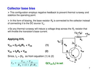
![Collector base bias
Advantages:
Better stabilization compared to fixed bias
Disadvantages:
This circuit provides negative feedback which reduces the gain of the amplifier.
Usage:
The feedback also decreases the input impedance of the amplifier as seen from
the base, which can be advantageous. Due to the gain reduction from feedback, this
biasing form is used only when the trade-off for stability is warranted.
8
How the bias stability is improved in collector base bias?
If IC becomes larger than design value, it causes an increase voltage drop
across RC hence smaller value of VCE which in turn causes IB to be smaller than
its design value. Since IC = βIB thus IC will also tend to be reduced towards its
original value.
biasing form is used only when the trade-off for stability is warranted.
]
)
1
(
[
C
B
BE
CC
C
R
R
V
V
I
β
β
+
+
−
=
C
BE
CC
C
R
V
V
I
−
=
If RB βRC
For bais Stabilization : RB βRC](https://image.slidesharecdn.com/lec-7-221021173633-143109d3/85/Lec-7-pdf-8-320.jpg)


This document discusses biasing schemes and stability of BJT transistors. It describes four common biasing schemes - fixed bias, collector base bias, voltage divider bias, and emitter bias. Voltage divider bias is the most widely used as it provides both biasing and stabilization. Stabilization is important to prevent thermal runaway from temperature and parameter variations. The stability factor S indicates how sensitive the collector current is to changes in the collector-base leakage current. Lower S provides better stability.


![Bipolar Junction Transistor Biasing [Types]](https://cdn.slidesharecdn.com/ss_thumbnails/ele307module2working-1-251030220651-e41b5c93-thumbnail.jpg?width=640&height=640&fit=bounds)