1. Transistor biasing involves setting the proper zero signal collector current and maintaining the proper collector-emitter voltage during signal passage. This is done to ensure faithful amplification.
2. If a transistor is not properly biased, it will work inefficiently and distort the output signal. Biasing can be done with a battery or biasing circuit associated with the transistor.
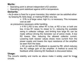
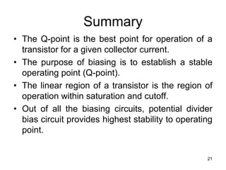
3. Proper biasing sets the operating point in the active region and aims to keep it stable despite temperature changes or other variations, through techniques like negative feedback. The potential divider bias circuit is commonly used due to its stability.
The document summarizes different classes of power amplifiers: Class A amplifiers conduct through the full 360 degrees of the input signal with the Q-point set in the middle of the load line. Class B amplifiers conduct through 180 degrees of the input with the Q-point at 0V. Class AB is a compromise between A and B, conducting between 180-360 degrees with the Q-point between the midpoint and cutoff. Class C conducts less than 180 degrees with the Q-point below cutoff. Class D is biased for digital signals and has high efficiency.
Power Amplifier circuits.
Output stages of types of power amplifier (class A, class B, class AB, class C, class D)
Distortions( Harmonic and Crossover).
Push-pull amplifier with and without transformer.
Complimentary symmetry and Quasi- complimentary symmetry push pull amplifier.
1) Biasing is important in transistors to prevent saturation or cutoff. Voltage divider bias uses resistors in a potential divider configuration to provide stable biasing.
2) In common emitter configuration, the input is between base and emitter, and output is between collector and emitter. The input characteristics show base current vs base-emitter voltage, and output characteristics show collector current vs collector-emitter voltage.
3) A document describing an electronics assignment covering topics on transistor biasing circuits, characteristics, and configurations. Diagrams and equations are provided as answers to questions.
1. Low-pass filters allow low frequencies to pass through but attenuate frequencies higher than the cutoff frequency. They are implemented using a resistor and capacitor in conjunction with an op-amp amplifier.
2. A first-order low-pass filter has a single RC pair and rolls off at -20dB per decade above the cutoff frequency. Higher-order filters use multiple RC stages to achieve steeper roll-offs such as -40dB per decade for a second-order filter.
3. The cutoff frequency is the frequency at which the gain is 3dB below the maximum and is inversely proportional to the product of the resistor and capacitor values in each stage.
Here are the steps to solve this:
1) VZ = VBE3 (zener voltage is equal to BJT base-emitter voltage)
2) Using KVL: -VZ + VBE3 + IE3RE = 0
3) Simplify: IE3RE = 0
4) IE3 is constant
Therefore, with a zener diode replacing R2, the current IE3 (and thus IT) remains constant regardless of load or temperature variations. The zener diode acts to stabilize the BJT base-emitter voltage, keeping the current constant.
Class A amplifiers have the highest linearity because the transistor is always conducting. They are the least efficient at 30% due to continuous power loss. Class B amplifiers only conduct for half of the signal cycle, improving efficiency to 50% but introducing crossover distortion. Class AB balances efficiency and distortion by conducting more than half but less than the full cycle. Class C amplifiers have the greatest efficiency of 80% but introduce heavy distortion as they conduct for less than half of the input cycle. They are used for radio frequency amplification rather than audio.
in this slide you will learn what are classes of amplifiers and what is main difference between all classes of amplifier
and after reading this slide you will be able to explain all clases of amplifier
A power amplifier is designed to provide maximum power output and is used to amplify weak signals to a level sufficient to drive a loudspeaker or other output device. It consists of multiple stages, with the final stage designed specifically for high power output. Power amplifiers use power transistors that can handle large currents and dissipate significant heat. They are classified based on the operating mode of the transistors, including class A, B, AB, and C power amplifiers. Transformer coupling is commonly used to match impedances in power amplifier circuits.
Bjt(common base ,emitter,collector) from university of central punjabKhawaja Shazy
The document discusses the bipolar junction transistor (BJT) and its three configurations: common base, common emitter, and common collector.
1. A BJT consists of three terminals - collector, base, and emitter - and comes in two types, npn and pnp, depending on whether it has two n-type and one p-type semiconductor or two p-type and one n-type.
2. The common base configuration has zero phase shift/angle and high input impedance and output impedance. Common emitter has 180 degree phase shift and is most commonly used due to its high current and voltage gain. Common collector is also called emitter follower and has low output imped
Class AB amplifiers combine aspects of Class A and Class B amplifiers. They are biased so both transistors conduct for small signals like Class A for lower distortion, and for large signals only one transistor conducts at a time like Class B for higher efficiency. The circuit uses a voltage divider and diodes to bias the transistors into slight conduction even without an input signal. This overcomes crossover distortion. The output operates with the Q-point slightly above cutoff and ac cutoff at the supply voltage for Class AB operation between Class A and Class B.
Direct coupled amplifiers amplify lower frequencies by directly connecting the output of one transistor stage to the input of the next without any coupling components. They have a simple circuit arrangement with minimal components, making them low cost. However, they cannot amplify high frequencies and are susceptible to operating point shifts from temperature variations. Direct coupled amplifiers are well-suited for applications requiring low frequency or low current amplification such as photoelectric or thermoelectric sensors.
Introduction to operational Amplifier. For A2 level physics (CIE). Discusses characteristics of op amp, inverting and non inverting amplifier, and voltage follower, and transfer characetristics, virtual earth , etc
There are four main methods of transistor biasing: base resistor method, emitter bias method, biasing with collector feedback resistor, and voltage-divider bias method. The document then focuses on explaining the base resistor method and voltage-divider bias method in more detail. For the base resistor method, a resistor is used to provide base current, but it has poor stability. For the voltage-divider bias method, two resistors are used to provide stable biasing of the transistor by controlling the base-emitter voltage. This method is widely used due to its stability from the emitter resistor preventing changes in collector current.
This document discusses power amplifiers classified as Class A amplifiers. It describes the basic operation of a Class A amplifier, in which the collector current is always nonzero, resulting in low maximum efficiency of 25%. It covers the DC and AC analyses of a basic common-emitter Class A amplifier and a transformer-coupled Class A amplifier. The transformer-coupled configuration allows for a higher theoretical maximum efficiency of 50% by keeping the operating point very close to the supply voltage. However, practical efficiencies are still typically less than 40% due to losses in the transformer.
A voltage regulator is a circuit that creates and maintains a fixed output voltage, irrespective of changes to the input voltage or load conditions. Voltage regulators (VRs) keep the voltages from a power supply within a range that is compatible with the other electrical components. While voltage regulators are most commonly used for DC/DC power conversion, some can perform AC/AC or AC/DC power conversion as well. This article will focus on DC/DC voltage regulators.
Amplifier classes of operation and biasing networks latestHrudya Balachandran
This document discusses different classes of amplifier operation and biasing networks. It covers:
- Amplifier classes are defined by the conduction angle of the active device during the input cycle, including Class A (360 degrees), Class B (180 degrees), Class C (less than 180 degrees), and Class AB (more than 180 degrees but less than 360 degrees).
- Biasing networks are needed to set the operating conditions of active devices and can be passive (using resistors) or active (using additional active components for better temperature stability).
- Passive networks are simple but have poor temperature stability while active networks are more complex but provide excellent temperature stability from shared heat sinking of components.
Rectifier converts alternating current (AC) to direct current (DC). There are two main types of rectifiers: half wave and full wave. Half wave rectifiers only conduct current during one half of the AC cycle, resulting in lower power output. Full wave rectifiers conduct current during both halves of the AC cycle, doubling the output frequency and power compared to half wave rectifiers. Common full wave rectifier circuits include the center tap and bridge rectifier.
This document discusses Class B amplifiers. It explains that Class B amplifiers use two transistors to conduct for alternating half cycles of the input signal, improving efficiency over Class A amplifiers. The theoretical maximum efficiency of a Class B amplifier is 78.5%. Circuit diagrams of common-collector and push-pull Class B amplifier configurations are presented, along with their input/output waveforms and operating principles. Distortion caused by crossover regions when the input signal is low is also discussed.
1) CE amplifiers use bias circuits to set an operating point for the transistor. Simple bias circuits vary with transistor parameters like beta.
2) Load line analysis graphs the interplay between circuit constraints and the transistor output characteristic to determine the operating point.
3) Stabilized bias circuits aim to fix the emitter current independently of beta using an emitter resistor and potential divider bias network. Negative feedback bias circuits also use feedback from the collector voltage.
A multistage transistor amplifier contains more than one stage of amplification. In a multistage amplifier, a number of single amplifiers are connected together. There are three main types of multistage transistor amplifiers: R-C coupled amplifiers use capacitors to couple stages, transformer coupled amplifiers use transformers, and direct coupled amplifiers directly connect stages without isolation. Transformer coupling provides excellent impedance matching and higher gain compared to other types. The gain of a multistage amplifier is equal to the product of the gains of the individual stages.
This document describes different types of oscillators. It discusses oscillators that use positive feedback to generate AC signals at a desired frequency. It provides block diagrams and explanations of RC phase shift oscillators, Wein bridge oscillators, Hartley oscillators, Colpitts oscillators, and Clapp oscillators. Equations for calculating the oscillation frequency of each type of oscillator are also presented.
This document provides an overview of active filters, including their basic types and terminology. The four basic types of active filters are low-pass, high-pass, band-pass, and band-stop (notch) filters. Key terms discussed include poles, order, Butterworth, Chebyshev, and Bessel filters. Circuit configurations for single-pole and two-pole (Sallen-Key) low-pass and high-pass filters are presented.
This document discusses power amplifiers and class A amplifiers. It begins with an introduction to power amplifiers, including their purpose of delivering high power to low resistance loads. It then covers classification of amplifiers based on conduction angle and efficiency ratings. The document analyzes class A amplifiers in detail, including derivation of input power, output power, and efficiency equations. It shows the efficiency of class A amplifiers is limited to 25% theoretically due to continuous conduction. Examples are provided to demonstrate calculations for input power, output power, and efficiency.
This presentation is based on the subject electric power system.Circle diagram of transmission line.In this presentation two topics covered about the circle diagram of transmission line.It is about the medium and long transmission line circle diagram.Receiving-end circle diagram and sending-end circle diagram of the transmission line.This presentation help you to the improve knowledge about the transmission line circle diagram.
The document provides information about operational amplifiers (op-amps). It defines an op-amp as a high-gain amplifier consisting of differential and other stages used to amplify signals and perform math functions. Key characteristics are very high differential gain, high input impedance, low output impedance. The document outlines op-amp components like inputs, outputs, power supplies. It describes stages within an op-amp like the input, intermediate, level shifting and output stages. Performance parameters discussed include input offset voltage, input resistance, open loop gain, output resistance and more. Closed loop and open loop op-amp configurations are explained.
FREQUENCY ENTRAINMENT IN A WIEN BRIDGE OSCILLATORSwgwmsaBoro
1. The document reports on a student project studying the frequency of a Wien bridge oscillator.
2. It introduces the Wien bridge oscillator and how it produces continuous oscillations using an RC feedback network and amplifier.
3. The students analyze the frequency of their Wien bridge oscillator circuit experimentally and find that frequencies above 1MHz cannot be achieved due to limitations of the op-amp used.
The potential divider bias circuit provides the most stable operating point (Q-point) for a transistor. It uses two resistors (R1 and R2) in a potential divider configuration to set the base voltage, and a third resistor (RE) connected from the emitter to ground introduces negative feedback. This feedback makes the Q-point nearly independent of temperature variations and transistor parameter changes, providing the highest stability of any biasing circuit.
The document discusses transistor biasing and stabilization. It defines biasing as establishing a quiescent point (Q-point) for the transistor in the active region through supply voltages and resistances. This allows distortion-free amplification. Thermal runaway occurs when increased collector current further increases junction temperature, leading to uncontrollable positive feedback. Several biasing circuits are described, including fixed bias, emitter feedback bias, collector-to-base feedback bias, collector-emitter feedback bias, and voltage divider/emitter bias. Stability factor is a measure of how sensitive the collector current is to changes in the transistor's reverse saturation current. Voltage divider bias establishes a Q-point independently of beta through a resistor
Transistor biasing circuits establish a quiescent operating point (Q-point) for the transistor in the active region to produce distortion-free amplification. Five common biasing circuits are described: fixed bias, emitter feedback bias, collector feedback bias, collector-emitter feedback bias, and self/emitter bias. The self/emitter bias circuit forms a voltage divider with external resistors to set the base voltage independently of beta, improving stability against temperature variations and beta changes between transistors. Stability is quantified by the stability factor and improved by increasing the emitter resistor relative to the base resistor.
Biasing is the process of applying external voltages to transistors to ensure proper operation. It involves forward or reverse biasing transistor junctions to place the device in specific regions like active, saturation, or cutoff. Common biasing circuits include fixed bias using a base resistor, collector-to-base bias which provides feedback, and emitter bias where a resistor is added to stabilize operating point. Proper biasing establishes a quiescent point and load line on the transistor characteristics curve for linear amplification.
This document discusses transistor biasing circuits. It outlines different types of biasing circuits including fixed bias, emitter bias, collector feedback bias, and voltage divider bias. It explains how each circuit works, analyzing key parameters like collector current, collector-emitter voltage, and stability factor. The goal of biasing circuits is to set the transistor's operating point in the active region for faithful signal amplification while stabilizing it against temperature and other variations. Voltage divider bias is highlighted as the most widely used method due to its ability to stabilize the operating point through negative feedback.
1) Bipolar junction transistors (BJTs) are commonly used semiconductor devices that can be used as amplifiers and logic switches. They consist of three terminals: collector, base, and emitter.
2) There are several types of biasing circuits that can be used with BJTs, including fixed bias, collector feedback bias, fixed bias with emitter resistor, and voltage divider biasing. Biasing circuits ensure that the BJT operates in its active region.
3) The characteristics curves of different biasing circuits show how voltages and currents vary with each other. Mathematical equations can be derived to describe the relationships between voltages and currents for different biasing configurations.
This document discusses transistor amplifiers. It describes how transistors can be used to amplify signals, with common configurations including common base, common collector, and common emitter. It then focuses on the common emitter transistor amplifier, providing circuit diagrams and explaining its input and output characteristics. Different types of transistor biasing are covered, including fixed, collector to base, voltage divider, and emitter biasing. The document also discusses small signal operation and models like the hybrid-pi and T models. It explains load line analysis and concepts like the dc and ac load lines. Finally, it covers bias stability and factors that can affect an amplifier's operating point.
Pre Final Year project/ mini project for Electronics and communication engine...Shirshendu Das
The document describes a project to construct a full wave rectifier circuit that converts 220V AC input into 5V, -5V, and variable 5V DC output. It includes a center tapped transformer, bridge rectifier using 4 diodes, and voltage regulators. Capacitor filters are used to obtain smooth DC waveforms from the pulsating rectified output. The circuit is simulated using NI Multisim software and experimental results are analyzed. Positive 5V output is obtained using an LM7805 regulator, negative 5V output uses an LM7905 regulator, and an LM317 provides adjustable output.
BJT Biasing for B.Tech Ist Year EngineeringRaghav Bansal
Okay, let's solve this step-by-step:
1) Given: IC = 2 mA
2) We're told IC = βIB
3) So we can set up and solve for β:
IC = βIB
2 mA = βIB
β = IC/IB = 2 mA / 0.5 mA = 4
So the answer for part a is:
β = 4
4) We're also given: IB = 0.5 mA
5) Using the voltage divider formula:
VB = VCC * (RB2 / (RB1 + RB2))
6) We know: VB = 0.7 V (for the B-
discussing differences faithful and un- faithful amplification
discussing stabilition in transistors
and how temperature affect collector current
discussing various methods of transistor biasing like
Base resister method ,Emitter Base method , Biasing with collector feedback method , Voltage divider bias
This document contains notes on transistor amplifiers. It begins by defining terms like voltage gain, current gain, and power gain. It then provides explanations of different transistor configurations including common-base, common-emitter, and common-collector. Circuit diagrams and explanations of single-stage and multistage RC coupled amplifiers are provided. The document also discusses topics like frequency response curves, types of coupling, classifications of power amplifiers, and comparisons of different amplifier classes. Questions and answers on these topics are included throughout.
Bipolar junction transistor characterstics biassing and amplification, lab 9kehali Haileselassie
This document summarizes an experiment on characterizing the input and output properties of a bipolar junction transistor (BJT) and demonstrating its signal amplification capabilities. The experiment involved establishing the transistor's DC operating point, then evaluating its small-signal AC operation. Key results included measuring the transistor's DC current gain and small-signal voltage gain, which compared reasonably well to theoretical predictions. The document also discussed the different regions of BJT operation and their implications for circuit applications.
Bipolar junction transistor characterstics biassing and amplification, lab 9kehali Haileselassie
This document summarizes an experiment on characterizing the input and output properties of a bipolar junction transistor (BJT) and demonstrating its ability to amplify signals when biased in the active region. Key findings include:
1) Measured voltages and currents matched predicted values closely, both from hand calculations and PSPICE simulations.
2) In the active region, a small AC input signal produced a larger AC output signal, demonstrating amplification. Measured gains matched predictions from an equivalent circuit model.
3) BJT regions of interest - active, cutoff, and saturation - were explored. In the active region the BJT acts as a current source, enabling its use as a signal amplifier.
This document provides an overview of bipolar junction transistors (BJT) including:
- The basic structure of an NPN or PNP transistor with emitter, base, and collector layers.
- How transistors operate in cutoff, saturation, and active modes depending on biasing of the PN junctions.
- How a small base current controls a larger collector current in the active region, allowing transistors to function as electronic switches or amplifiers.
1. The document discusses control strategies for EHV AC and DC transmission systems, including desired features of HVDC system control, control characteristics of constant current and constant extinction angle, and parallel operation of AC and DC systems.
2. Control of HVDC systems is achieved through control of current or voltage to maintain a constant voltage in the DC link. Common control modes include constant current control at the rectifier and constant extinction angle control at the inverter.
3. Parallel operation of AC and DC systems can present problems but also advantages; control coordination is needed between the two different transmission types.
Current mode circuits & voltage mode circuits Kevin Gajera
This document discusses current mode and voltage mode circuits. It begins by defining voltage mode and current mode circuits, noting that the definitions are not entirely precise as every circuit has both voltages and currents. It then provides examples of current mode circuits including the bipolar junction transistor and current mirror. It discusses how current mode and voltage mode signaling works for interconnects in integrated circuits. It notes several advantages of current mode circuits including lower power consumption and higher speed. It also discusses differences between the two modes and reasons for switching to current mode circuits such as easier compensation and better operation in continuous and discontinuous conduction modes. Potential disadvantages of current mode are also outlined like current sensing challenges and subharmonic oscillations.
This document discusses transistor biasing and faithful signal amplification in transistors. It begins by explaining that the basic function of a transistor is amplification, and that for faithful amplification the input circuit must remain forward biased and the output circuit must remain reverse biased during the signal. This is achieved through transistor biasing, which provides the proper zero-signal collector current, base-emitter voltage, and collector-emitter voltage. Several common biasing circuits are described, including base resistor, collector feedback resistor, and voltage divider methods. The key requirements for faithful amplification and the effects of improper biasing are illustrated. Transistor characteristics like the input curve and output curve are also discussed.
DC biasing applies fixed voltages to transistors to place them in an operating region for amplification. The operating point defines the transistor's quiescent operating conditions under DC. Stability refers to a circuit's insensitivity to parameter variations like temperature. Emitter-stabilized and voltage divider biasing improve stability over fixed biasing by incorporating an emitter or voltage divider resistor. Feedback biasing further increases stability by introducing negative feedback from collector to base.
An improved modulation technique suitable for a three level flying capacitor ...IJECEIAES
This research paper introduces an innovative modulation technique for controlling a 3-level flying capacitor multilevel inverter (FCMLI), aiming to streamline the modulation process in contrast to conventional methods. The proposed
simplified modulation technique paves the way for more straightforward and
efficient control of multilevel inverters, enabling their widespread adoption and
integration into modern power electronic systems. Through the amalgamation of
sinusoidal pulse width modulation (SPWM) with a high-frequency square wave
pulse, this controlling technique attains energy equilibrium across the coupling
capacitor. The modulation scheme incorporates a simplified switching pattern
and a decreased count of voltage references, thereby simplifying the control
algorithm.
Comparative analysis between traditional aquaponics and reconstructed aquapon...bijceesjournal
The aquaponic system of planting is a method that does not require soil usage. It is a method that only needs water, fish, lava rocks (a substitute for soil), and plants. Aquaponic systems are sustainable and environmentally friendly. Its use not only helps to plant in small spaces but also helps reduce artificial chemical use and minimizes excess water use, as aquaponics consumes 90% less water than soil-based gardening. The study applied a descriptive and experimental design to assess and compare conventional and reconstructed aquaponic methods for reproducing tomatoes. The researchers created an observation checklist to determine the significant factors of the study. The study aims to determine the significant difference between traditional aquaponics and reconstructed aquaponics systems propagating tomatoes in terms of height, weight, girth, and number of fruits. The reconstructed aquaponics system’s higher growth yield results in a much more nourished crop than the traditional aquaponics system. It is superior in its number of fruits, height, weight, and girth measurement. Moreover, the reconstructed aquaponics system is proven to eliminate all the hindrances present in the traditional aquaponics system, which are overcrowding of fish, algae growth, pest problems, contaminated water, and dead fish.
Advanced control scheme of doubly fed induction generator for wind turbine us...IJECEIAES
This paper describes a speed control device for generating electrical energy on an electricity network based on the doubly fed induction generator (DFIG) used for wind power conversion systems. At first, a double-fed induction generator model was constructed. A control law is formulated to govern the flow of energy between the stator of a DFIG and the energy network using three types of controllers: proportional integral (PI), sliding mode controller (SMC) and second order sliding mode controller (SOSMC). Their different results in terms of power reference tracking, reaction to unexpected speed fluctuations, sensitivity to perturbations, and resilience against machine parameter alterations are compared. MATLAB/Simulink was used to conduct the simulations for the preceding study. Multiple simulations have shown very satisfying results, and the investigations demonstrate the efficacy and power-enhancing capabilities of the suggested control system.
Applications of artificial Intelligence in Mechanical Engineering.pdfAtif Razi
Historically, mechanical engineering has relied heavily on human expertise and empirical methods to solve complex problems. With the introduction of computer-aided design (CAD) and finite element analysis (FEA), the field took its first steps towards digitization. These tools allowed engineers to simulate and analyze mechanical systems with greater accuracy and efficiency. However, the sheer volume of data generated by modern engineering systems and the increasing complexity of these systems have necessitated more advanced analytical tools, paving the way for AI.
AI offers the capability to process vast amounts of data, identify patterns, and make predictions with a level of speed and accuracy unattainable by traditional methods. This has profound implications for mechanical engineering, enabling more efficient design processes, predictive maintenance strategies, and optimized manufacturing operations. AI-driven tools can learn from historical data, adapt to new information, and continuously improve their performance, making them invaluable in tackling the multifaceted challenges of modern mechanical engineering.
Electric vehicle and photovoltaic advanced roles in enhancing the financial p...IJECEIAES
Climate change's impact on the planet forced the United Nations and governments to promote green energies and electric transportation. The deployments of photovoltaic (PV) and electric vehicle (EV) systems gained stronger momentum due to their numerous advantages over fossil fuel types. The advantages go beyond sustainability to reach financial support and stability. The work in this paper introduces the hybrid system between PV and EV to support industrial and commercial plants. This paper covers the theoretical framework of the proposed hybrid system including the required equation to complete the cost analysis when PV and EV are present. In addition, the proposed design diagram which sets the priorities and requirements of the system is presented. The proposed approach allows setup to advance their power stability, especially during power outages. The presented information supports researchers and plant owners to complete the necessary analysis while promoting the deployment of clean energy. The result of a case study that represents a dairy milk farmer supports the theoretical works and highlights its advanced benefits to existing plants. The short return on investment of the proposed approach supports the paper's novelty approach for the sustainable electrical system. In addition, the proposed system allows for an isolated power setup without the need for a transmission line which enhances the safety of the electrical network
Optimizing Gradle Builds - Gradle DPE Tour Berlin 2024Sinan KOZAK
Sinan from the Delivery Hero mobile infrastructure engineering team shares a deep dive into performance acceleration with Gradle build cache optimizations. Sinan shares their journey into solving complex build-cache problems that affect Gradle builds. By understanding the challenges and solutions found in our journey, we aim to demonstrate the possibilities for faster builds. The case study reveals how overlapping outputs and cache misconfigurations led to significant increases in build times, especially as the project scaled up with numerous modules using Paparazzi tests. The journey from diagnosing to defeating cache issues offers invaluable lessons on maintaining cache integrity without sacrificing functionality.
Discover the latest insights on Data Driven Maintenance with our comprehensive webinar presentation. Learn about traditional maintenance challenges, the right approach to utilizing data, and the benefits of adopting a Data Driven Maintenance strategy. Explore real-world examples, industry best practices, and innovative solutions like FMECA and the D3M model. This presentation, led by expert Jules Oudmans, is essential for asset owners looking to optimize their maintenance processes and leverage digital technologies for improved efficiency and performance. Download now to stay ahead in the evolving maintenance landscape.
Batteries -Introduction – Types of Batteries – discharging and charging of battery - characteristics of battery –battery rating- various tests on battery- – Primary battery: silver button cell- Secondary battery :Ni-Cd battery-modern battery: lithium ion battery-maintenance of batteries-choices of batteries for electric vehicle applications.
Fuel Cells: Introduction- importance and classification of fuel cells - description, principle, components, applications of fuel cells: H2-O2 fuel cell, alkaline fuel cell, molten carbonate fuel cell and direct methanol fuel cells.
2. 2
Transistor Biasing
The basic function of transistor is amplification. The process of raising the
strength of weak signal without any change in its general shape is
referred as faithful amplification. For faithful amplification it is essential
that:-
1. Emitter-Base junction is forward biased
2. Collector- Base junction is reversed biased
3. Proper zero signal collector current
The proper flow of zero signal collector current and the
maintenance of proper collector emitter voltage during the
passage of signal is called transistor biasing.
3. 3
WHY BIASING?
If the transistor is not biased properly, it would work inefficiently and
produce distortion in output signal.
HOW A TRANSISTOR CAN BE BIASED?
A transistor is biased either with the help of battery or associating a
circuit with the transistor. The later method is more efficient and is
frequently used. The circuit used for transistor biasing is called the
biasing circuit.
4. 4
BIAS STABILITY
Through proper biasing, a desired quiescent operating point of the transistor
amplifier in the active region (linear region) of the characteristics is obtained. It is
desired that once selected the operating point should remain stable. The
maintenance of operating point stable is called Stabilisation.
The selection of a proper quiescent point generally depends on the following
factors:
(a) The amplitude of the signal to be handled by the amplifier and distortion
level in signal
(b) The load to which the amplifier is to work for a corresponding supply
voltage
The operating point of a transistor amplifier shifts mainly with changes in
temperature, since the transistor parameters — β, ICO and VBE (where the
symbols carry their usual meaning)—are functions of temperature.
5. 5
The DC Operating Point
For a transistor circuit to amplify it must be properly biased with dc
voltages. The dc operating point between saturation and cutoff is
called the Q-point. The goal is to set the Q-point such that that it
does not go into saturation or cutoff when an a ac signal is applied.
6. 6
Requirements of biasing network
• Ensuring proper zero signal collector current.
• Ensuring VcE not falling below 0.5V for Ge transistor and 1V for Silicon
transistor at any instant.
• Ensuring Stabilization of operating point. (zero signal IC and VcE)
7. 7
The Thermal Stability of Operating Point (SIco)
Stability Factor S:- The stability factor S, as the change of collector
current with respect to the reverse saturation current, keeping β and
VBE constant. This can be written as:
The Thermal Stability Factor : SIco
SIco = ∂Ic
∂Ico
This equation signifies that Ic Changes SIco times as fast as Ico
Differentiating the equation of Collector Current IC = (1+β)Ico+ βIb &
rearranging the terms we can write
SIco ═ 1+β
1- β (∂Ib/∂IC)
It may be noted that Lower is the value of SIco better is the stability
Vbe, β
8. 8
Various Biasing Circuits
• Fixed Bias Circuit
• Fixed Bias with Emitter Resistor
• Collector to Base Bias Circuit
• Potential Divider Bias Circuit
9. 9
The Fixed Bias Circuit
15 V
C
E
B
15 V
200 k 1 k
The Thermal Stability Factor : SIco
SIco = ∂Ic
∂Ico
General Equation of SIco Comes out to be
SIco ═ 1 + β
1- β (∂Ib/∂IC)
Vbe, β
Applying KVL through Base Circuit we can
write, Ib Rb+ Vbe= Vcc
Diff w. r. t. IC, we get (∂Ib / ∂Ic) = 0
SIco= (1+β) is very large
Indicating high un-stability
Ib
Rb
RC
RC
10. 10
Merits:
• It is simple to shift the operating point anywhere in the active region by
merely changing the base resistor (RB).
• A very small number of components are required.
Demerits:
• The collector current does not remain constant with variation in
temperature or power supply voltage. Therefore the operating point is
unstable.
• When the transistor is replaced with another one, considerable change in
the value of β can be expected. Due to this change the operating point will
shift.
• For small-signal transistors (e.g., not power transistors) with relatively high
values of β (i.e., between 100 and 200), this configuration will be prone to
thermal runaway. In particular, the stability factor, which is a measure of
the change in collector current with changes in reverse saturation current,
is approximately β+1. To ensure absolute stability of the amplifier, a
stability factor of less than 25 is preferred, and so small-signal transistors
have large stability factors.
11. 11
Usage:
• Due to the above inherent drawbacks, fixed bias is rarely used in linear
circuits (i.e., those circuits which use the transistor as a current source).
Instead, it is often used in circuits where transistor is used as a switch.
However, one application of fixed bias is to achieve crude automatic gain
control in the transistor by feeding the base resistor from a DC signal
derived from the AC output of a later stage.
12. 12
The fixed bias circuit is modified
by attaching an external resistor
to the emitter. This resistor
introduces negative feedback
that stabilizes the Q-point.
Fixed bias with emitter resistor
13. 13
Merits:
• The circuit has the tendency to stabilize operating point against
changes in temperature and β-value.
Demerits:
• As β-value is fixed for a given transistor, this relation can be satisfied
either by keeping RE very large, or making RB very low.
If RE is of large value, high VCC is necessary. This increases cost
as well as precautions necessary while handling.
If RB is low, a separate low voltage supply should be
used in the base circuit. Using two supplies of different
voltages is impractical.
• In addition to the above, RE causes ac feedback which reduces the
voltage gain of the amplifier.
Usage:
The feedback also increases the input impedance of the amplifier when
seen from the base, which can be advantageous. Due to the above
disadvantages, this type of biasing circuit is used only with careful
consideration of the trade-offs involved.
14. 14
The Collector to Base Bias Circuit
VCC
RC
C
E
B
RF
Ic
Ib
VBE
+
- IE
This configuration employs negative
feedback to prevent thermal runaway and
stabilize the operating point. In this form of
biasing, the base resistor RF is connected to
the collector instead of connecting it to the
DC source Vcc. So any thermal runaway will
induce a voltage drop across the Rc resistor
that will throttle the transistor's base current.
15. 15
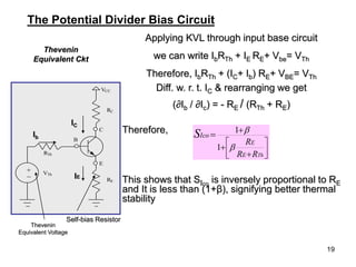
Applying KVL through base circuit
we can write (Ib+ IC) RC + Ib Rf+ Vbe= Vcc
Diff. w. r. t. IC we get
(∂Ib / ∂Ic) = - RC / (Rf + RC)
Therefore, SIco ═ (1+ β)
1+ [βRC/(RC+ Rf)]
Which is less than (1+β), signifying better thermal stability
16. 16
Merits:
• Circuit stabilizes the operating point against variations in temperature
and β (i.e. replacement of transistor)
Demerits:
• As β -value is fixed (and generally unknown) for a given transistor, this
relation can be satisfied either by keeping Rc fairly large or making Rf very
low.
If Rc is large, a high Vcc is necessary, which increases
cost as well as
precautions necessary while handling.
If Rf is low, the reverse bias of the collector–base region is
small, which limits the range of collector voltage swing that
leaves the transistor in active mode.
•The resistor Rf causes an AC feedback, reducing the voltage
gain of the amplifier. This undesirable effect is a trade-off for
greater Q-point stability.
Usage: The feedback also decreases the input impedance of the amplifier
as seen from the base, which can be advantageous. Due to the gain
reduction from feedback, this biasing form is used only when the trade-off
for stability is warranted.
17. 17
This is the most commonly used arrangement for biasing as it provide good
bias stability. In this arrangement the emitter resistance ‘RE’ provides
stabilization. The resistance ‘RE’ cause a voltage drop in a direction so as to
reverse bias the emitter junction. Since the emitter-base junction is to be
forward biased, the base voltage is obtained from R1-R2 network. The net
forward bias across the emitter base junction is equal to VB- dc voltage drop
across ‘RE’. The base voltage is set by Vcc and R1 and R2. The dc bias
circuit is independent of transistor current gain. In case of amplifier, to avoid
the loss of ac signal, a capacitor of large capacitance is connected across
RE. The capacitor offers a very small reactance to ac signal and so it passes
through the condensor.
The Potential Divider Bias Circuit
18. 18
VCC
RC
C
E
B
VCC
R1
RE
R2
IE
IC
Ib
The Potential Divider Bias Circuit
To find the stability of this circuit we have
to convert this circuit into its Thevenin’s
Equivalent circuit
Rth = R1*R2 & Vth = Vcc R2
R1+R2 R1+R2
VCC
RC
C
E
B
VCC
R1
RE
R2
Rth = R1*R2 & Vth = Vcc R2
R1+R2 R1+R2
Rth = R1*R2 & Vth = Vcc R2
R1+R2 R1+R2
Rth = R1*R2 & Vth = Vcc R2
R1+R2 R1+R2
19. 19
Applying KVL through input base circuit
we can write IbRTh + IE RE+ Vbe= VTh
Therefore, IbRTh + (IC+ Ib) RE+ VBE= VTh
Diff. w. r. t. IC & rearranging we get
(∂Ib / ∂Ic) = - RE / (RTh + RE)
Therefore,
This shows that SIco
is inversely proportional to RE
and It is less than (1+β), signifying better thermal
stability
Thevenin
Equivalent Ckt
Th
R
R
R
E
E
Ico
S
1
1
The Potential Divider Bias Circuit
VCC
RC
C
E
B
RE
RTh
VTh
_
+
Thevenin
Equivalent Voltage
Self-bias Resistor
IE
Ib
IC
20. 20
Merits:
• Operating point is almost independent of β variation.
• Operating point stabilized against shift in temperature.
Demerits:
• As β-value is fixed for a given transistor, this relation can be satisfied either
by keeping RE fairly large, or making R1||R2 very low.
If RE is of large value, high VCC is necessary. This increases
cost as well
as precautions necessary while handling.
If R1 || R2 is low, either R1 is low, or R2 is low, or both are
low. A low R1 raises VB closer to VC, reducing the available
swing in collector voltage, and limiting how large RC can be
made without driving the transistor out of active mode. A low
R2 lowers Vbe, reducing the allowed collector current.
Lowering both resistor values draws more current from the
power supply and lowers the input resistance of the amplifier
as seen from the base.
AC as well as DC feedback is caused by RE, which reduces
the AC voltage gain of the amplifier. A method to avoid AC
feedback while retaining DC feedback is discussed below.
Usage:
The circuit's stability and merits as above make it widely used for linear
circuits.
21. 21
Summary
• The Q-point is the best point for operation of a
transistor for a given collector current.
• The purpose of biasing is to establish a stable
operating point (Q-point).
• The linear region of a transistor is the region of
operation within saturation and cutoff.
• Out of all the biasing circuits, potential divider
bias circuit provides highest stability to operating
point.