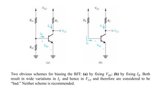
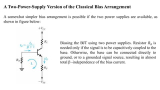
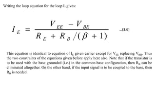
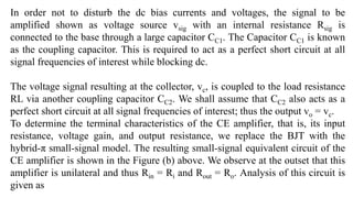
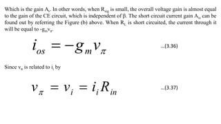
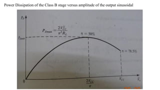
1) Biasing transistor amplifiers involves establishing a stable DC operating point. Two common biasing schemes for BJTs, fixing VBE or IB, result in wide variations in collector current IC due to temperature and β variations.
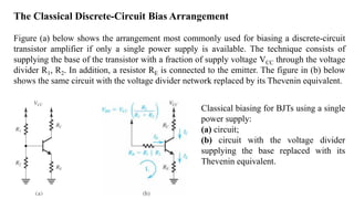
2) The classical discrete BJT bias arrangement uses a voltage divider to supply the base with a fraction of the supply voltage VCC. Resistors are selected to make the emitter current IE insensitive to temperature and β variations.
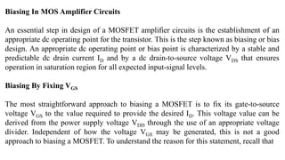
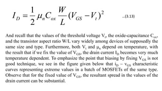
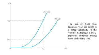
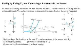
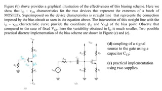
3) For MOSFET amplifiers, biasing by fixing the gate-source voltage VGS is not good because drain current ID depends on temperature-sensitive parameters. A better technique is to fix the gate voltage VG and connect a degenerative

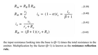
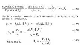
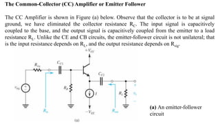
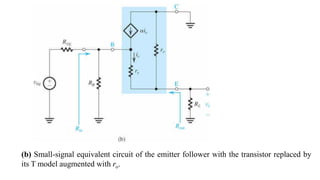
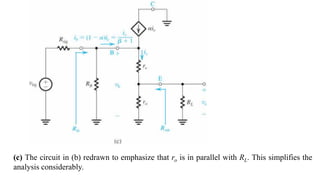
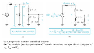
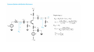
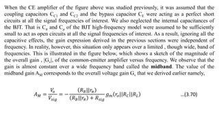
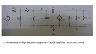
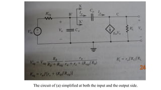
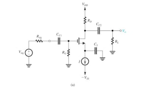
![To find the overall voltage gain Gv, we first apply Thevenin theorem at the input side of the
circuit in Figure (a) above to simplify it to the form in Figure (b). From the latter circuit we
see that vo can be found by utilizing the voltage divider rule; thus,
L
o
e
B
sig
L
o
B
sig
B
v
R
r
r
R
R
R
r
R
R
R
G
||
(
)
1
(
)
||
(
)
||
)(
1
(
We observe that the voltage gain is less than unity; however, for RB >> Rsig and (β+1)[re + (ro
|| RL)] >> (Rsig || RB), it becomes very close to unity. Thus the voltage at the emitter (vo)
follows very closely the voltage at the input, which gives the circuit the name emitter
follower.
…(3.69)](https://image.slidesharecdn.com/2820-231013030002-8c0bb0d7/85/2820-pdf-61-320.jpg)


![Bipolar Junction Transistor Biasing [Types]](https://cdn.slidesharecdn.com/ss_thumbnails/ele307module2working-1-251030220651-e41b5c93-thumbnail.jpg?width=640&height=640&fit=bounds)


