Downloaded 234 times


This document provides an overview of the 8251A USART chip, including: - It is a programmable peripheral designed for serial communication that converts parallel data from the CPU to serial and vice versa. - It has sections for the data bus buffer, read/write control logic, modem control, transmitter and receiver. - The transmitter accepts parallel data and converts it to serial, while the receiver accepts serial data and converts it to parallel for the CPU. - It has control, status and data registers that are accessed via various control signals to read/write data and control the chip's operation.
Introduction to G.H. Raisoni College and a brief overview of the 8251A USART functionality.
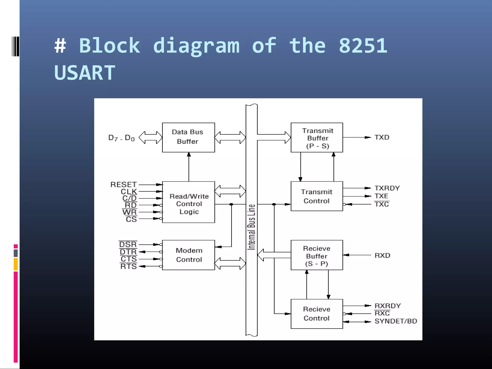
Presentation of the pin diagram and block diagram for the 8251A USART to illustrate architecture.
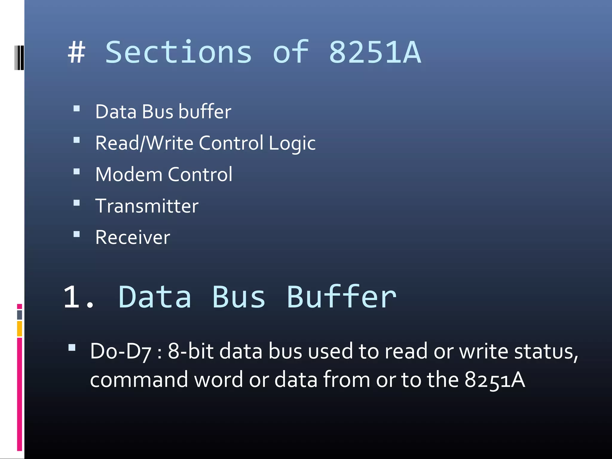
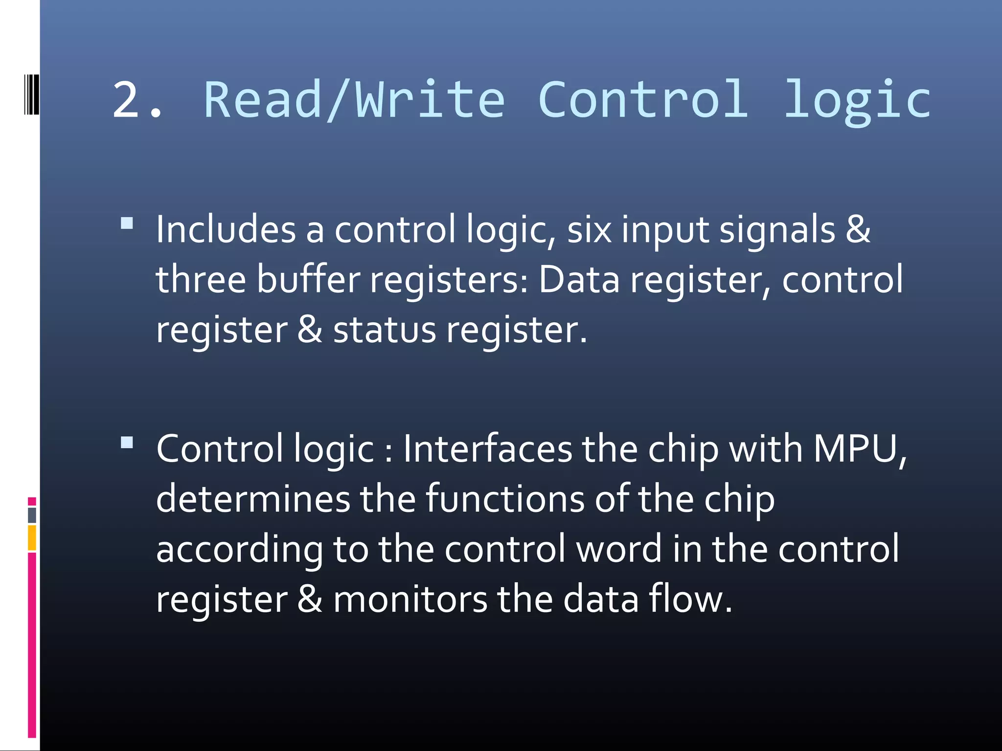
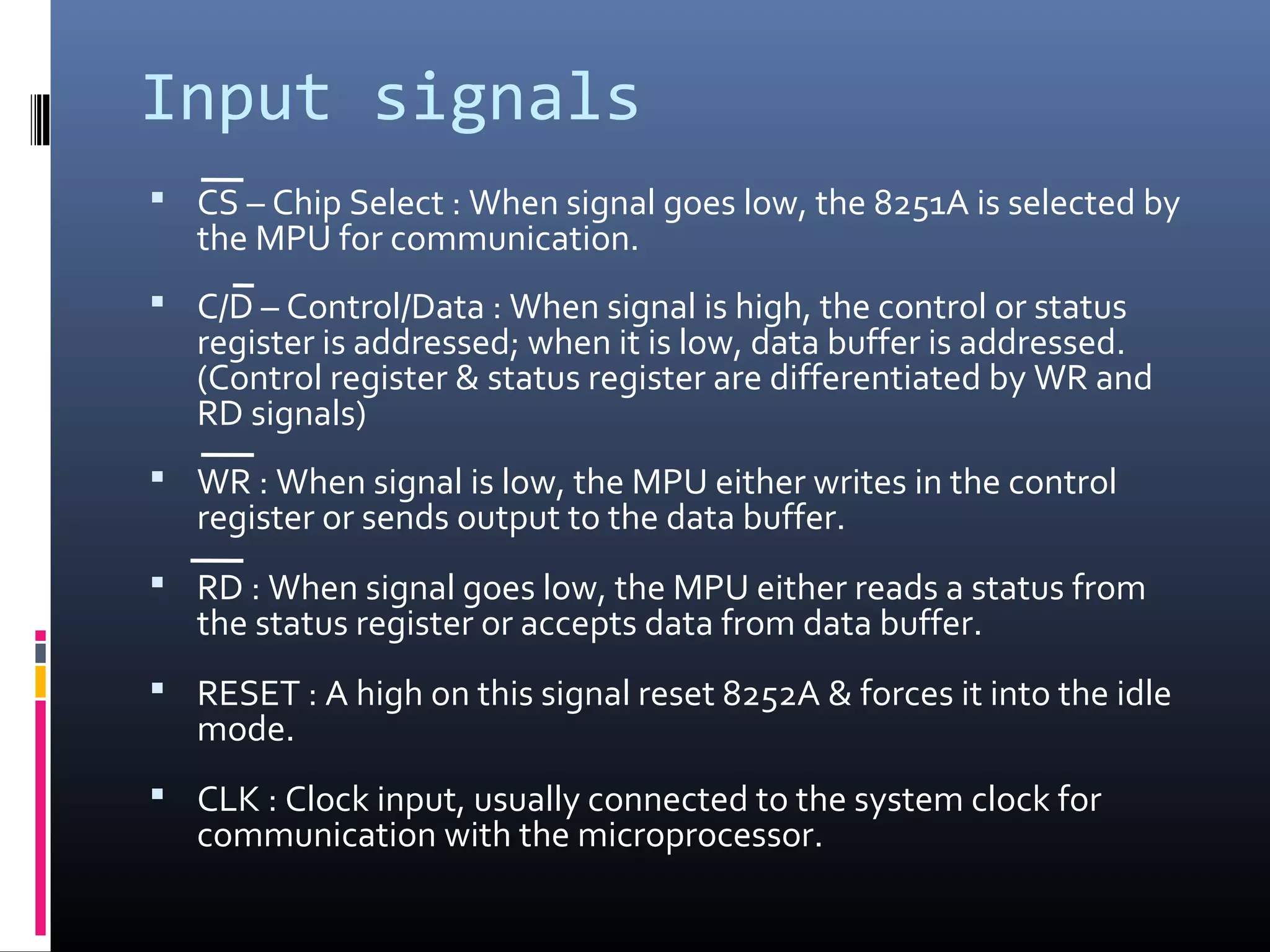
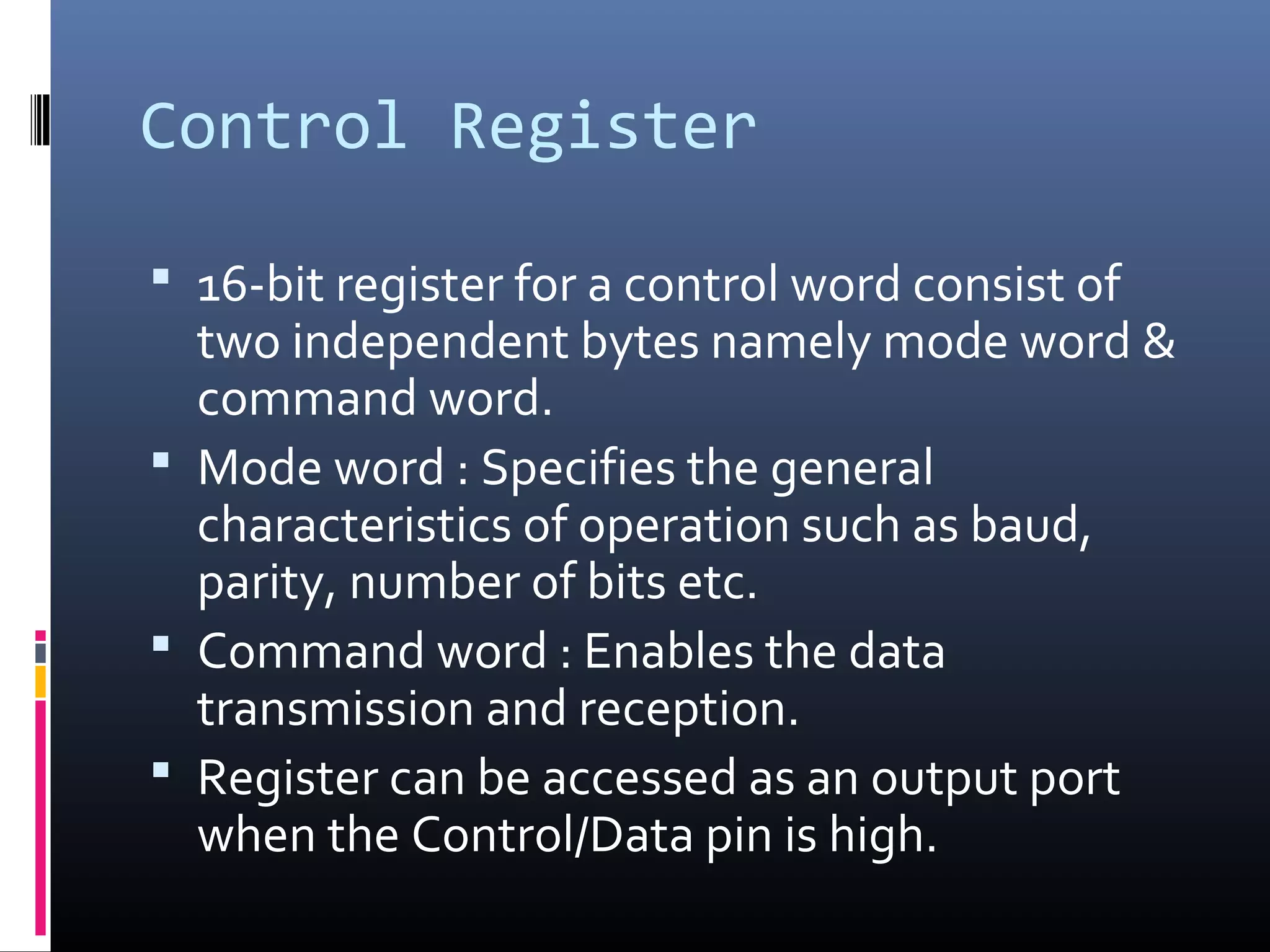
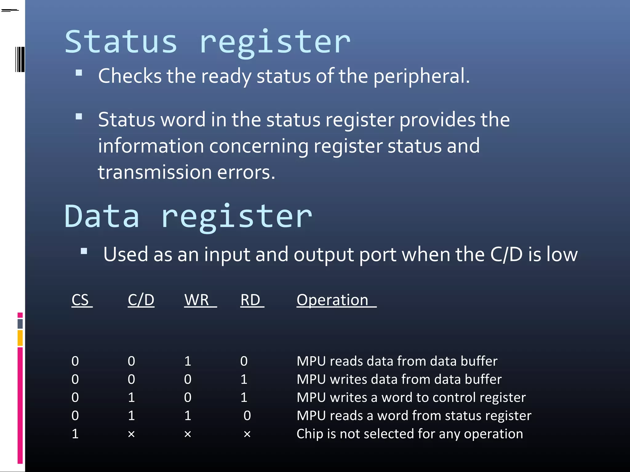
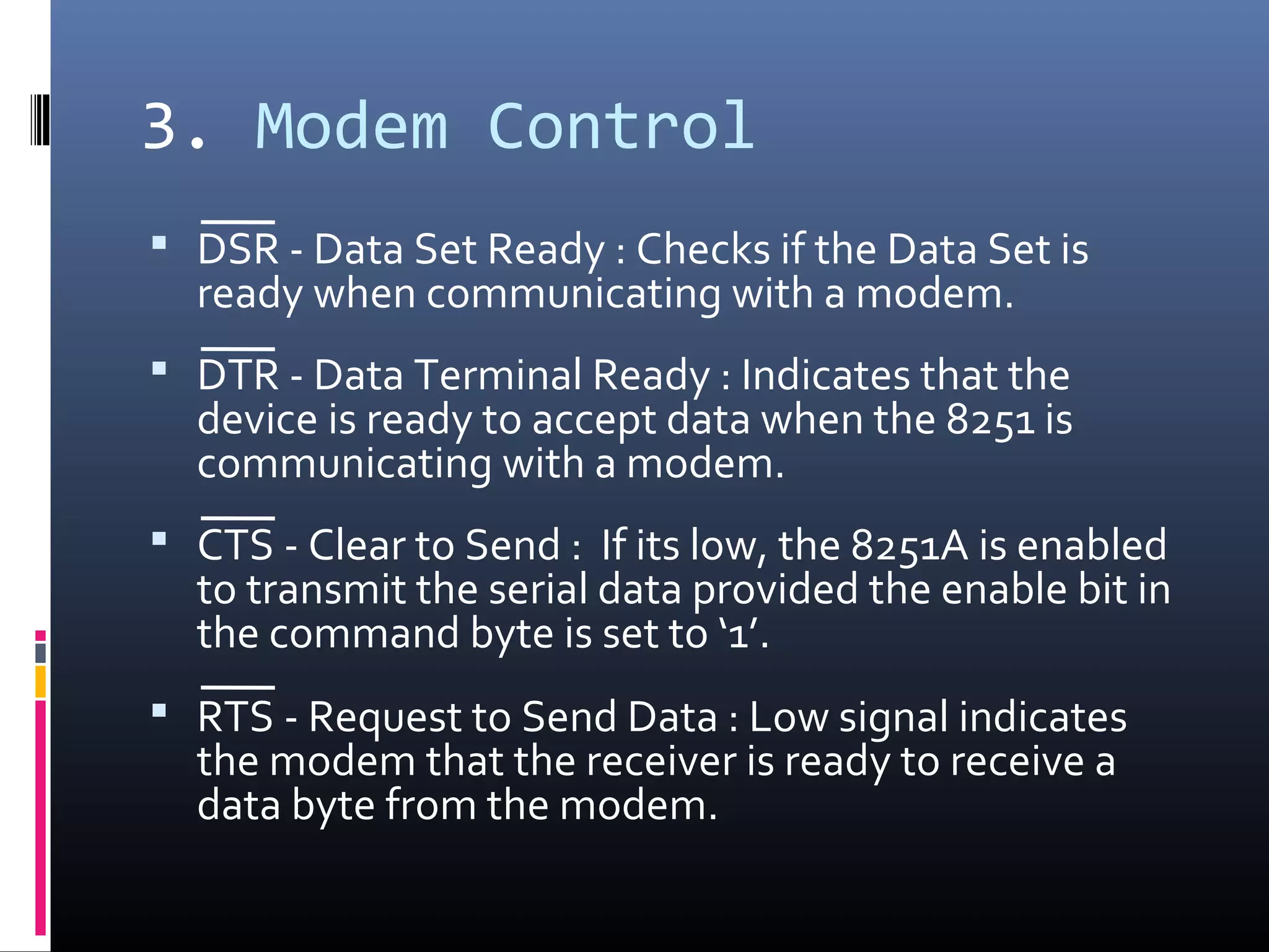
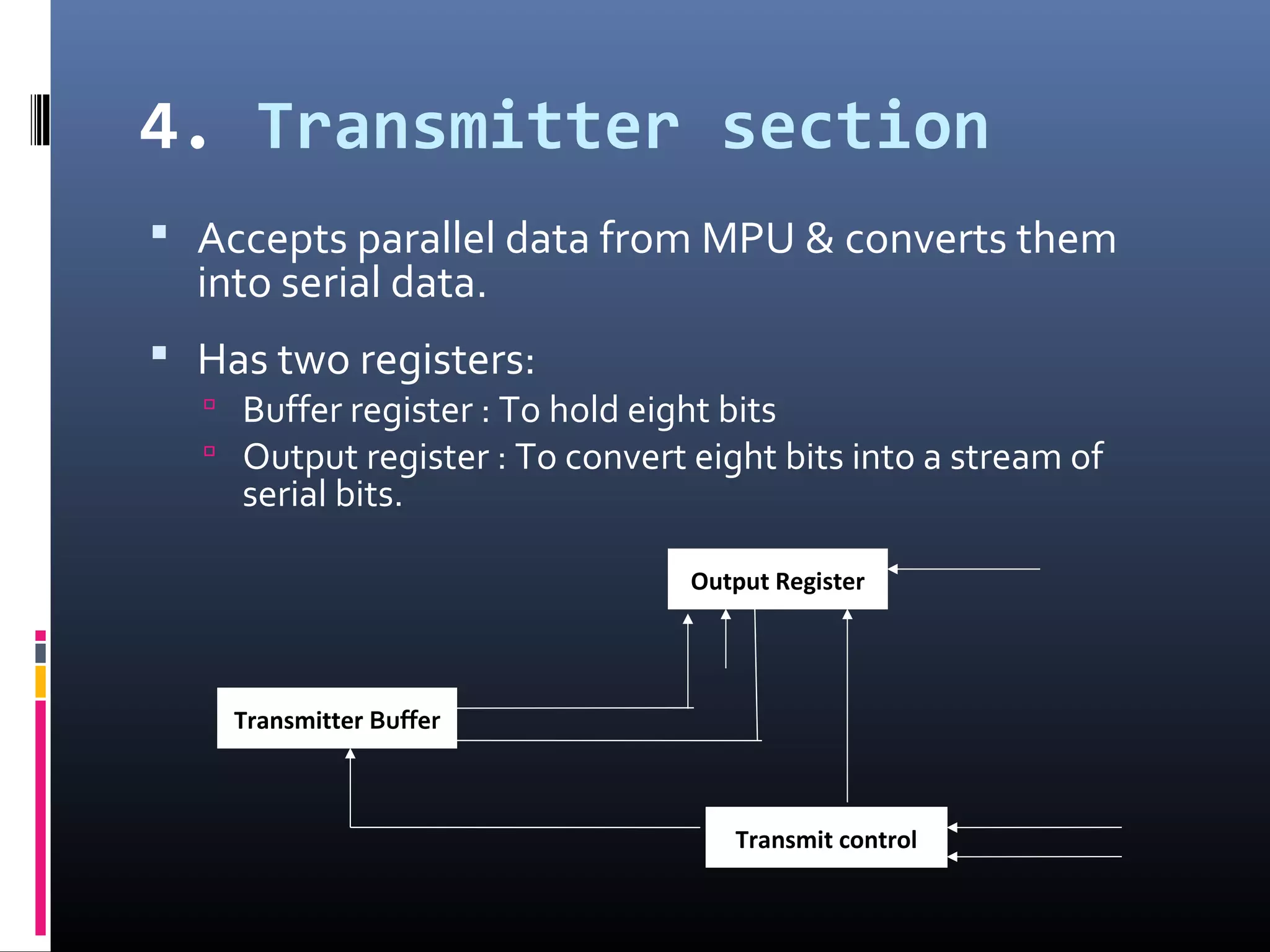
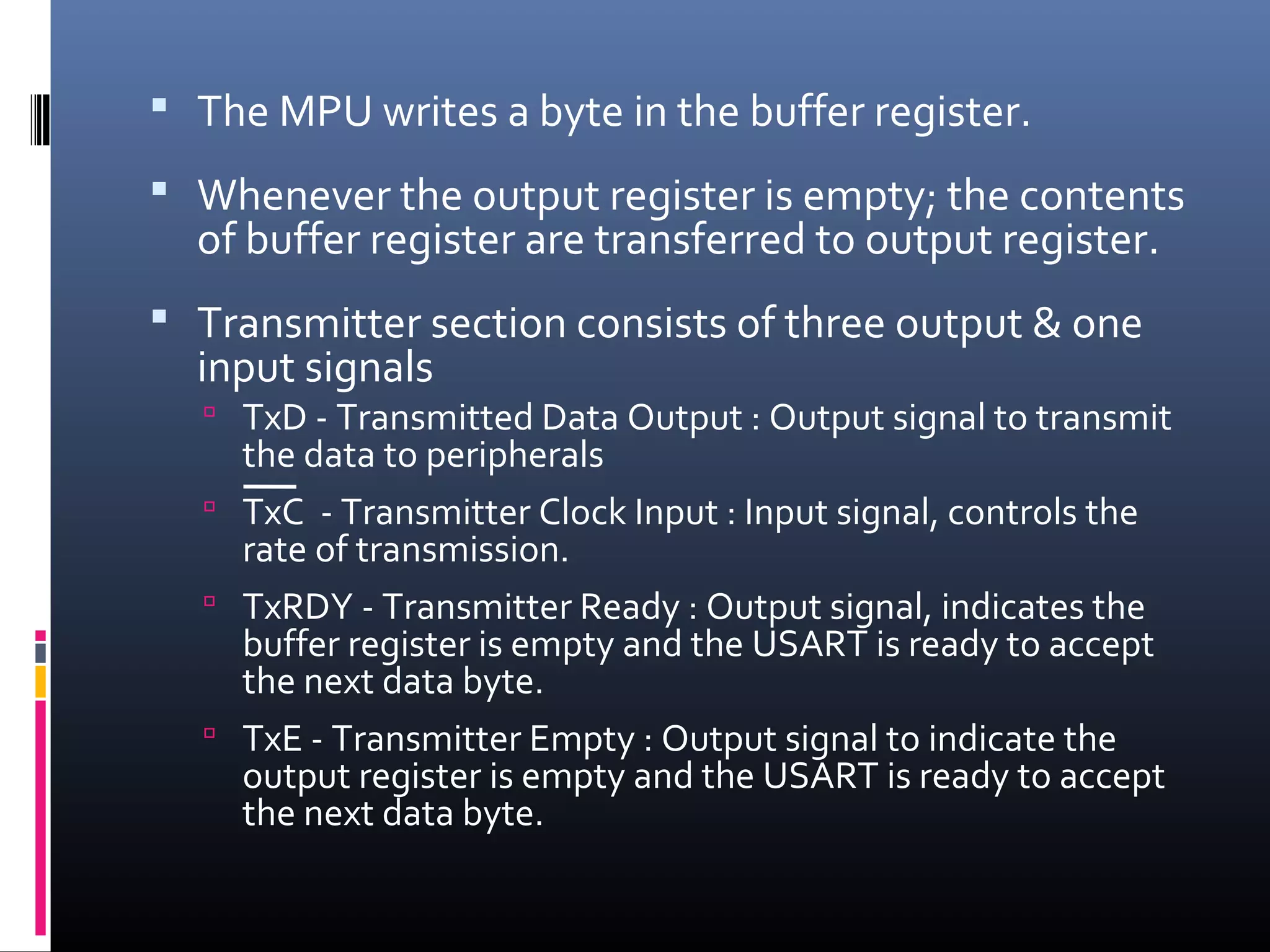
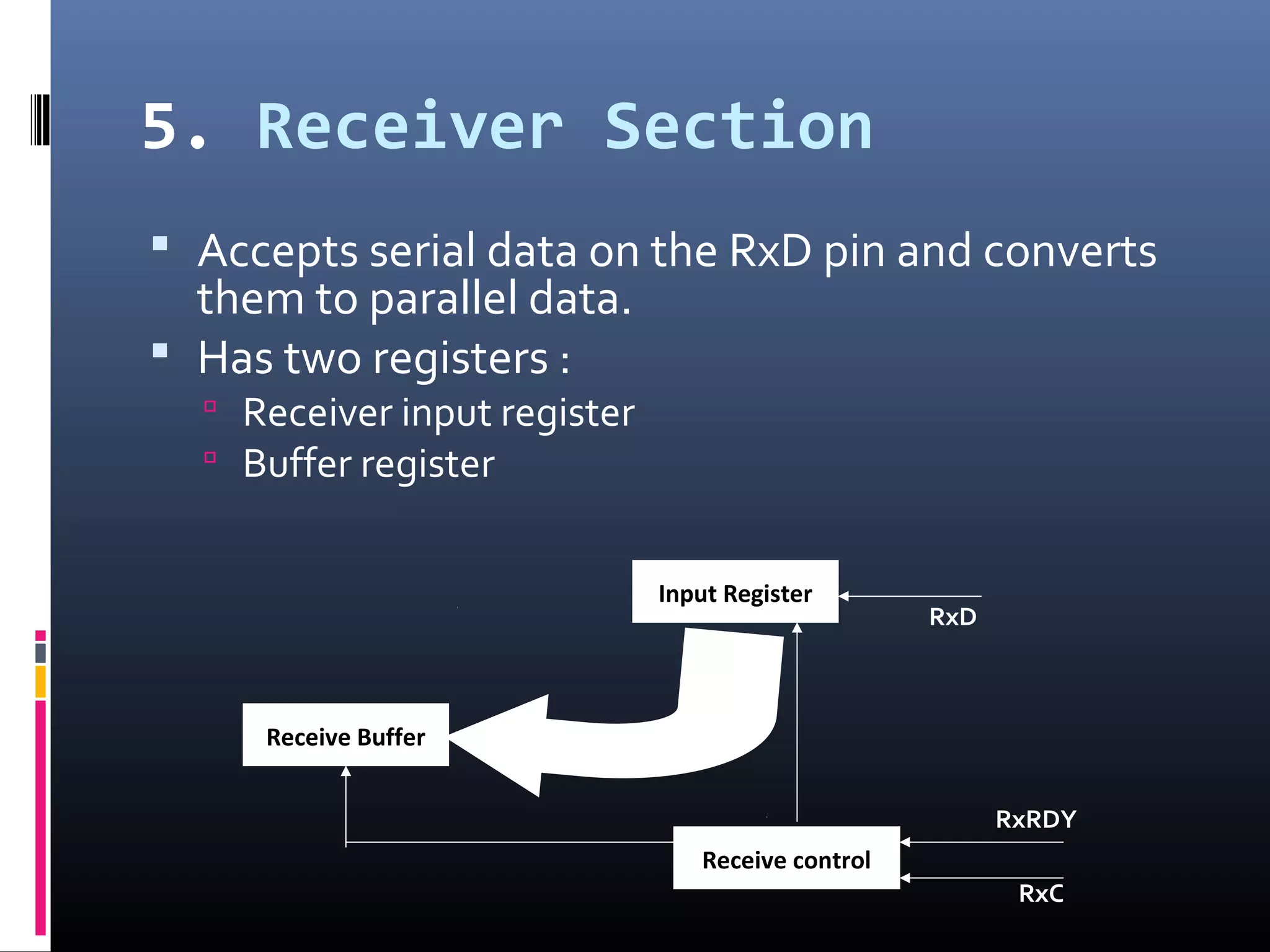
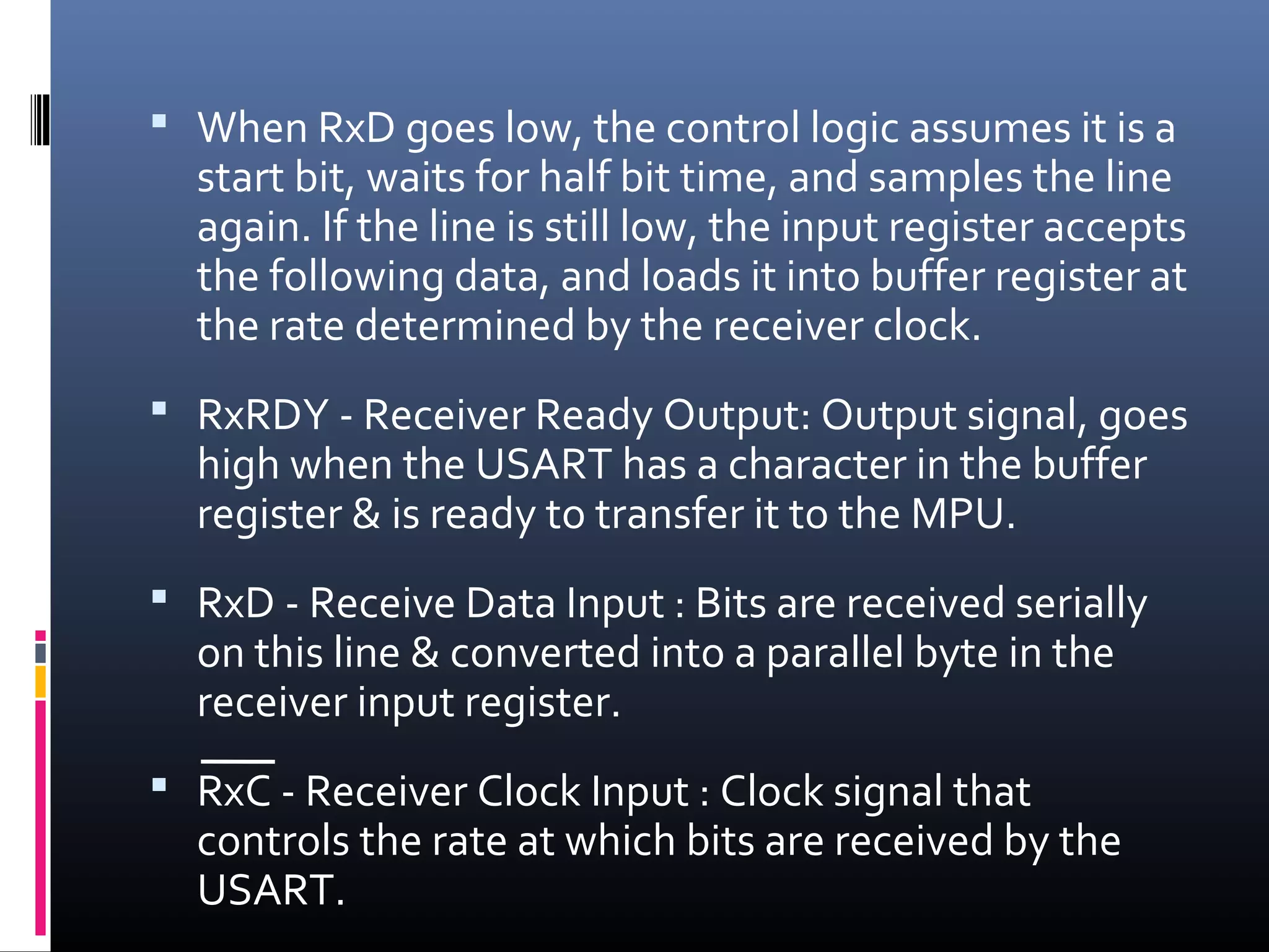
Detailed breakdown of the sections: Data Bus Buffer, Control Logic, Modem Control, Transmitter, and Receiver.
Closing slide with a simple expression of gratitude.