SlideShare a Scribd company logo
1 of 15
Page 1 of 15
Microprocessor & Interfacing Notes By Er. Swapnil V. Kaware (svkaware@yahoo.co.in)
Chapter No. 03. Interfacing Devices I
Q(1). Draw & explain block diagram of 8259 PIC?.
Interrupt Request Register (IRR):-
The interrupts at IRQ input lines are handled by Interrupt Request Register internally. IRR
stores all the interrupt requests in it in order to serve them one by one on the priority basis.
In-Service Register (ISR):-
This stores all the interrupt requests those are being served, i.e. ISR keeps a track of the
requests being served.
Priority Resolver:-
This unit determines the priorities of the interrupt requests appearing simultaneously. The
highest priority is selected and stored into the corresponding bit of ISR during INTA pulse. The
IR0 has the highest priority while the IR7 has the lowest one, normally in fixed priority mode.
The priorities however may be altered by programming the 8259 in rotating priority mode.
Interrupt Mask Register (IMR):-
This register stores the bits required to mask the interrupt puts. IMR operates on IRR at the
direction of the Priority Resolver.
Page 2 of 15
Microprocessor & Interfacing Notes By Er. Swapnil V. Kaware (svkaware@yahoo.co.in)
Interrupt Control Logic:-
This block manages the interrupt and interrupt acknowledge sigD8ls to be sent to the CPU for
serving one of the eight interrupt requests. This also accepts interrupt acknowledge (INTA)
signal from CPU that causes the 8259 to release vector address on to the data bus.
Data Bus Buffer:-
This tri-state bidirectional buffer interfaces internal 8259 bus to the microprocessor system
data bus. Control words, status and vector information pass through buffer during read or write
operations.
Read write Control Logic:-
This circuit accepts and decodes commands from the CPU. This also allows the status of the
8259 to be transferred on to the data bus.
Cascade Buffer/Comparator:-
The three I/O pins CAS0-2 are outputs when the 8259 is used as a master. The same pins act as
inputs when the 8259 is in slave mode. The 8259 in master mode sends the ID of the
interrupting slave device on these lines. The slave thus selected, will send its pre programmed
vector address on the data bus during the next INTA pulse.
CS:-
This is an active-low chip select signal for enabling RD and WR operations of 8259. INTA
function is independent of CS.
WR:-
This pin is an active-low write enable input to 8259. This enables it to accept command words
from CPU.
RD:-
This is an active-low read enable input to 8259. A low on this line enables 8259 to release
status onto the data bus of CPU. D7-D0 These pins form a bidirectional data bus that carries 8-
bit data either to control word or from status word registers.
CASo-CAS2:-
Cascade Lines A single 8259 provides eight vectored interrupts. If more interrupts are required,
the 8259 is used in cascade mode. In cascade mode, a master 8259 along with eight slaves 8259
Page 3 of 15
Microprocessor & Interfacing Notes By Er. Swapnil V. Kaware (svkaware@yahoo.co.in)
can provide up to 64 vectored interrupt lines. These three lines act as select lines for
addressing the slaves 8259.
SP/EN:-
This pin is a dual purpose pin. When the chip is used in buffered mode, it can be used as buffer
enable to control buffer trans-receivers. If this is not used in buffered mode then the pin is used
as input to designate whether the chip is used as a master (SP = 1) or a slave (EN = 0).
INT:-
This pin goes high whenever a valid interrupt request is asserted. This is used to interrupt the
CPU and is connected to the interrupt input of CPU.
IR0-IR7 (Interrupt requests):-
These pins act as inputs to accept interrupt requests to the CPU. In edge triggered mode, an
interrupt service is requested by raising an IR pin from a low to a high state and holding it high
until it is acknowledged, and just by latching it to high level, if used in level triggered mode.
Q(2). Explain command words of 8259 PIC?. OR
Q(3). Explain ICW1 and ICW3 in detail?.
The command words of 8259 are classified in two groups, viz. initialization command words
(ICWs) and operation command words (OCWs).
Initialization Command Words (ICWs):- If A0 = 0 and D4 = 1, the control word is recognized
as ICW1. It contains the control bits for edge/level triggered mode, single/cascade mode, call
address interval and whether ICW4 is required or not, etc.
If A0 = 1, the control word is recognized as ICW2. The ICW2 stores details
regarding interrupt vector addresses.
ICW1 and ICW2 are compulsory command words in initialization sequence of 8259 while
ICW3 and ICW4 are optional. The ICW3 is read only when there are more than one 8259 in the
system, i.e. cascading is used (SNGL = 0). The SNGL bit in ICW1 indicates whether the 8259 is in
cascade mode or not.
In master mode [i.e. SP = 1 or in buffer mode M/S = 1 in ICW4], the 8-bit slave register will be
set bit-wise to '1' for each slave in the system. The requesting slave will then release the second
byte of a CALL sequence.
In slave mode [i.e. SP=0 or if BUF=1 and M/S=0 in ICW4] bits D2 to D0 identify the slave, i.e.
000 to 111 for slave 1 to slave 8. The slave compares the cascade inputs with these bits and if
they are equal, the second byte if the CALL sequence is released by it on the data bus.
Page 4 of 15
Microprocessor & Interfacing Notes By Er. Swapnil V. Kaware (svkaware@yahoo.co.in)
Page 5 of 15
Microprocessor & Interfacing Notes By Er. Swapnil V. Kaware (svkaware@yahoo.co.in)
The use of this command word depends on the IC4 bit of ICW1. If IC4= 1, ICW4 is used,
otherwise it is neglected. The bit functions of ICW4 are described as follows:
SFNM Special fully nested mode is selected, if SFNM = 1.
(i). BUF If BUF = 1, the buffered mode is selected. In the buffered mode,
(ii). SP/EN acts as enable output and the master/slave is determined using the M/S bit of
ICW4.
(iii). If M/S = 1, 8259 is a master. If M/S = 0, 8259 is a slave. If BUF =0, M/S is to be neglected.
(iv). If AEOI = 1, the automatic end of interrupt mode is selected.
(v). If ÎĽPM=0, the Mcs-85 system operation is selected and if ÎĽPM =1, 8086/88 operation is
selected.
Q(4). Explain operating modes of 8259 PIC?.
The different modes of operation of 8259 can be programmed by setting or resting the
appropriate bits of the ICWs or OCWs. The different modes of operation of 8259 are explained
as,
(i). Fully Nested Mode:-
This is the default mode of operation of 8259. IR0 has the highest priority and IR7 has the
lowest one. When interrupt requests are noticed, the highest priority request amongst them is
determined and the vector is placed on the data bus.
The corresponding bit of ISR is set and remains set till the microprocessor issues
an EOI command just before returning from the service routine or the AEOI bit is set. If the ISR
(in service) bit is set, all the same or lower priority interrupts are inhibited but higher levels
will generate an interrupt, that will be acknowledged only if the microprocessor's interrupt
enable flag (IF) is set. The priorities can afterwards be changed by programming the rotating
priority modes.
(ii). End of Interrupt (EOI):-
The ISR bit can be reset either with AEOI bit of ICW1 or by EOI command, issued before
returning from the interrupt service routine. There are two types of EOI commands specific and
non-specific. When 8259 is operated in the modes that preserve fully nested structure, it can
determine which ISR bit is to be reset on EOT.
When nonspecific EOI command is issued to 8259 it will automatically reset the
highest ISR bit out of those already set. When a mode that may disturb the fully nested
structure is used, the 8259 is no longer able to determine the last level acknowledged. In this
case a specific EOI command is issued to reset a particular ISR bit. An ISR bit that is masked by
Page 6 of 15
Microprocessor & Interfacing Notes By Er. Swapnil V. Kaware (svkaware@yahoo.co.in)
the corresponding IMR bit, will not be cleared by a non-specific EOI of 8259, if it is in special
mask mode.
(iii). Automatic Rotation:-
This is used in the applications where all the interrupting devices are of equal priority. In this
mode, an interrupt request (IR) level receives lowest priority after it is served while the next
device to be served gets the highest priority in sequence. Once all the devices are served like
this, the first device again receives highest priority.
(iv). Automatic EOI Mode:-
Till AEOI = 1 in ICW4, the 8259 operates in AEOI mode. In this mode, the 8259 performs a non-
specific EOI operation at the trailing edge of the last INTA pulse automatically. This mode
should be used only when a nested multilevel interrupt structure is not required with a single
8259.
(v). Specific Rotation:-
In this mode a bottom priority level can be selected, using L2, L1 and L0 in OCW2 and R =1,
SL = 1, EOI = 0. The selected bottom priority fixes other priorities. If IR5 is selected as a bottom
priority, then IR5 will have least priority and IR4 will have a next higher priority. Thus IR6 will
have the highest priority. These priorities can be changed during an EOI command by
programming the rotate on specific EOI command in OCW2
(vi). Special Mask Mode:-
In special mask mode, when a mask bit is set in OCW1, it inhibits further interrupts at that level
and enables interrupt from other levels, which are not masked.
(vii). Edge and Level Triggered Mode:-
This mode decides whether the interrupt should be edge triggered or level triggered. If bit
LTIM of ICW1 = 0, they are edge triggered, otherwise the interrupts are level triggered. Reading
8259 Status The status of the internal registers of 8259 can be read using this mode. The
OCW3 is used to read IRR and ISR while OCW1 is used to
read IMR. Reading is possible only in no polled mode.
(viii). Poll Command:-
In polled mode of operation, the INT output of 8259 is neglected, though it functions normally,
by not connecting INT output or by masking INT input of the microprocessor. The poll mode is
entered by setting P =1 in OCW3. The 8259 is polled by using software execution by
microprocessor instead of the requests on INT input. The 8259 treats the next RD pulse to the
Page 7 of 15
Microprocessor & Interfacing Notes By Er. Swapnil V. Kaware (svkaware@yahoo.co.in)
8259 as an interrupt acknowledge. An appropriate ISR bit is set, if there is a request. The
priority level is read and a data word is placed on to data bus, after RD is activated
A poll command may give you more than 64 priority levels. Note that this has nothing to do
with the 8086 interrupt structure and the interrupt priorities.
(ix). Special Fully Nested Mode:-
This mode is used in more complicated systems, where cascading is used and the priority has to
be programmed in the master using ICW4. This is somewhat similar to the normal nested
mode. In this mode, when an interrupt request from a certain lave is in service, this slave can
further send requests to the master, if the requesting device connected to the slave has higher
priority than the one being currently served.
In this mode, the master interrupts the CPU only when the interrupting device has a
higher or the same priority than the one currently being served. In normal mode, other
requests than the one being served are masked out. When entering the interrupt service
routine the software has to check whether this is the only request from the slave. This is done
by sending a nonspecific
EOI command to the slave and then reading its ISR and checking for zero. If its
zero, a non-specific EOI can be sent to the master, otherwise no EOI should be sent. This mode
is important, since in the absence of this mode, the slave would interrupt the master only once
and hence the priorities of the 'lave inputs would have been disturbed.
(x). Buffered Mode:-
When the 8259 is used in the systems where bus driving buffers are used on data buses
(e.g. cascade systems). The problem of enabling the buffers exists. The 8259 sends buffer
enable signal on SP /EN pin, whenever data is placed on the bus.
(xii). Cascade Mode
The 8259 can be connected in a system containing one master and eight laves (maximum) to
handle up to 64 priority levels. The master controls the slaves using CAS0-CAS2 which act as
chip select inputs (encoded) for slaves. In this mode, the slave INT outputs are connected with
master IR inputs. When a slave request line is activated and acknowledged, the master will
enable the slave to release the vector address during second pulse of INTA sequence.
The cascade lines are normally low and contain slave address codes from the
trailing edge of the first INT A pulse to the trailing edge of the second INT A pulse. Each 8259 in
the system must be separately initialized and programmed to work in different modes. The EOI
command must be issued twice, one for master and the other for the slave. A separate address
decoder is used to activate the chip select line of each 8259.
Page 8 of 15
Microprocessor & Interfacing Notes By Er. Swapnil V. Kaware (svkaware@yahoo.co.in)
Q(5). Draw & explain block diagram/architecture of 8251 USART?.
The 8251 is a programmable chip designed for synchronous and asynchronous serial data
communication. The INTEL 8251 is the industry standard Universal Synchronous
Asynchronous Receiver Transmitter (USART) designed for data communications. The 8251 is
used as a peripheral device and is programmed by the CPU to operate using virtually any serial
data transmission technique.
The USART accepts data characters from the CPU in parallel format and then
converts them into a continuous serial data stream for transmission simultaneously; it can
receive serial data streams and convert them into parallel data character for the CPU. The
USART will signal the CPU whenever it can accept a new character for transmission or
whenever it has received a character for the CPU.
The block diagram includes five section,
(i). Read/write Control Logic, (ii). Transmitter,
(iii). Receiver, (iv). Modem Control,
(v). Data Bus Buffer.
Page 9 of 15
Microprocessor & Interfacing Notes By Er. Swapnil V. Kaware (svkaware@yahoo.co.in)
(i). Read/Write Control Logic:-
The control logic interfaces the chip with the processor, determines the functions of the chip
according to the control word in its register, and monitors the data flow.
(ii). Transmitter:-
The transmitter section converts a parallel word received from the processor into serial bits
and transmits them over the TxD line to a peripheral.
(iii). Receiver:-
The transmitter section receives serial bits from a peripheral, converts them into a parallel
word, and transfers the word to the ÎĽP.
(iv). Modem Control:-
The modem control is used to establish data communication through modems over telephone
lines.
(v). Data Bus Buffer:-
This bidirectional register can be addressed as an input and an output port when the pin is low.
The function of various signals of 8251 USART is as given below,
(a). D0 to D7 (l/O terminal):-
This is bidirectional data bus which receive control words and transmits data from the CPU and
sends status words and received data to CPU.
(b). RESET (Input terminal):-
A "High" on this input forces the 8251 into "reset status." The device waits for the writing of
"mode instruction." The min. reset width is six clock inputs during the operating status of CLK.
(c). CLK (Input terminal):-
CLK signal is used to generate internal device timing. CLK signal is independent of RXC or TXC.
However, the frequency of CLK must be greater than 30 times the RXC and TXC at Synchronous
mode and Asynchronous "x1" mode, and must be greater than 5 times at Asynchronous "x16"
and "x64" mode.
(d). WR (Input terminal):-
This is the "active low" input terminal which receives a signal for writing transmit data and
control words from the CPU into the 8251.
Page 10 of 15
Microprocessor & Interfacing Notes By Er. Swapnil V. Kaware (svkaware@yahoo.co.in)
(e). RD (Input terminal):-
This is the "active low" input terminal which receives a signal for reading receive data and
status words from the 8251.
(f). C/D (Input terminal):-
This is an input terminal which receives a signal for selecting data or command words and
status words when the 8251 is accessed by the CPU. If C/D = low, data will be accessed.
If C/D = high, command word or status word will be accessed.
(g). CS (Input terminal):-
This is the "active low" input terminal which selects the 8251 at low level when the CPU
accesses. Note: The device won’t be in "standby status"; only setting CS = High.
(h). TXD (output terminal):-
This is an output terminal for transmitting data from which serial-converted data is sent out.
The device is in "mark status" (high level) after resetting or during a status when transmit is
disabled. It is also possible to set the device in "break status" (low level) by a command.
(i). TXRDY (output terminal):-
This is an output terminal which indicates that the 8251is ready to accept a transmitted data
character. But the terminal is always at low level if CTS = high or the device was set in "TX
disable status" by a command.
Note: TXRDY status word indicates that transmit data character is receivable,
regardless of CTS or command. If the CPU writes a data character, TXRDY will be reset by the
leading edge or WR signal.
(j). TXEMPTY (Output terminal):-
This is an output terminal which indicates that the 8251 has transmitted all the characters and
had no data character. In "synchronous mode," the terminal is at high level, if transmit data
characters are no longer remaining and sync characters are automatically transmitted. If the
CPU writes a data character, TXEMPTY will be reset by the leading edge of WR signal.
Note : As the transmitter is disabled by setting CTS "High" or command, data
written before disable will be sent out. Then TXD and TXEMPTY will be "High". Even if a data is
written after disable, that data is not sent out and TXE will be "High". After the transmitter is
enabled, it sent out.
Page 11 of 15
Microprocessor & Interfacing Notes By Er. Swapnil V. Kaware (svkaware@yahoo.co.in)
(k). TXC (Input terminal):-
This is a clock input signal which determines the transfer speed of transmitted data. In
"synchronous mode," the baud rate will be the same as the frequency of TXC. In "asynchronous
mode", it is possible to select the baud rate factor by mode instruction. It can be 1, 1/16 or 1/64
the TXC. The falling edge of TXC sifts the serial data out of the 8251.
(l). RXD (input terminal):-
This is a terminal which receives serial data.
(m). RXRDY (Output terminal):-
This is a terminal which indicates that the 8251 contains a character that is ready to READ. If
the CPU reads a data character, RXRDY will be reset by the leading edge of RD signal. Unless the
CPU reads a data character before the next one is received completely, the preceding data will
be lost. In such a case, an overrun error flag status word will be set.
(n). RXC (Input terminal):-
This is a clock input signal which determines the transfer speed of received data. In
"synchronous mode," the baud rate is the same as the frequency of RXC. In "asynchronous
mode," it is possible to select the baud rate factor by mode instruction. It can be 1, 1/16, 1/64
the RXC.
(o). SYNDET/BD (Input or output terminal):-
This is a terminal whose function changes according to mode. In "internal synchronous mode."
this terminal is at high level, if sync characters are received and synchronized. If a status word
is read, the terminal will be reset. In "external synchronous mode, "this is an input terminal. A
"High" on this input forces the 8251 to start receiving data characters.
In "asynchronous mode," this is an output terminal which generates "high level"
output upon the detection of a "break" character if receiver data contains a "low-level" space
between the stop bits of two continuous characters. The terminal will be reset, if RXD is at high
level. After Reset is active, the terminal will be output at low level.
(p). DSR (Input terminal):-
This is an input port for MODEM interface. The input status of the terminal can be recognized
by the CPU reading status words.
(q). DTR (Output terminal):-
This is an output port for MODEM interface. It is possible to set the status of DTR by a
command.
Page 12 of 15
Microprocessor & Interfacing Notes By Er. Swapnil V. Kaware (svkaware@yahoo.co.in)
(r). CTS (Input terminal):-
This is an input terminal for MODEM interface which is used for controlling a transmit circuit.
The terminal controls data transmission if the device is set in "TX Enable" status by a command.
Data is transmittable if the terminal is at low level.
(s). RTS (Output terminal):-
This is an output port for MODEM interface. It is possible to set the status RTS by a command.
Q(6). Draw & explain mode register format for USART 8251 for synchronous and
asynchronous mode.
There are two types of control word,
1. Mode instruction (setting of function) & 2. Command (setting of operation)
1) Mode Instruction:-
Page 13 of 15
Microprocessor & Interfacing Notes By Er. Swapnil V. Kaware (svkaware@yahoo.co.in)
Mode instruction is used for setting the function of the 8251. Mode instruction will be in "wait
for write" at either internal reset or external reset. That is, the writing of a control word after
resetting will be recognized as a "mode instruction."
In the case of synchronous mode, it is necessary to write one-or two byte sync characters. If
sync characters were written, a function will be set because the writing of sync characters
constitutes part of mode instruction.
2) Command:-
Command is used for setting the operation of the 8251. It is possible to write a command
whenever necessary after writing a mode instruction and sync characters.
Page 14 of 15
Microprocessor & Interfacing Notes By Er. Swapnil V. Kaware (svkaware@yahoo.co.in)
Status Word:-
It is possible to see the internal status of the 8251 by reading a status word. The bit
configuration of status word is shown in Figure..
Page 15 of 15
Microprocessor & Interfacing Notes By Er. Swapnil V. Kaware (svkaware@yahoo.co.in)
***************************************** ALL THE BEST *****************************************

More Related Content

What's hot

Pin configuration of 8085
Pin configuration of 8085Pin configuration of 8085
Pin configuration of 8085
82338476
 
8251
82518251
8251
Aisu
 
Microprocessors 1-8086
Microprocessors 1-8086Microprocessors 1-8086
Microprocessors 1-8086
Shubham Chaurasia
 

What's hot (20)

Lect 5
Lect 5Lect 5
Lect 5
 
Minimum mode and Maximum mode Configuration in 8086
Minimum mode and Maximum mode Configuration in 8086Minimum mode and Maximum mode Configuration in 8086
Minimum mode and Maximum mode Configuration in 8086
 
8085
80858085
8085
 
Viva
VivaViva
Viva
 
8155 PPI
8155 PPI8155 PPI
8155 PPI
 
Timing diagram 8085 microprocessor
Timing diagram 8085 microprocessorTiming diagram 8085 microprocessor
Timing diagram 8085 microprocessor
 
8085 instruction-set part 1
8085 instruction-set part 18085 instruction-set part 1
8085 instruction-set part 1
 
8085 microprocessor Architecture and Pin description
8085 microprocessor Architecture and Pin description 8085 microprocessor Architecture and Pin description
8085 microprocessor Architecture and Pin description
 
Basics of peripheral devices and Working
Basics of peripheral devices and WorkingBasics of peripheral devices and Working
Basics of peripheral devices and Working
 
Interfacing of data converters & io devices
Interfacing of data converters & io devicesInterfacing of data converters & io devices
Interfacing of data converters & io devices
 
Pin configuration of 8085
Pin configuration of 8085Pin configuration of 8085
Pin configuration of 8085
 
advancsed microprocessor and interfacing
advancsed microprocessor and interfacingadvancsed microprocessor and interfacing
advancsed microprocessor and interfacing
 
Microprocessor Basics 8085 Ch-1
Microprocessor Basics 8085 Ch-1Microprocessor Basics 8085 Ch-1
Microprocessor Basics 8085 Ch-1
 
8251
82518251
8251
 
Microprocessors 1-8086
Microprocessors 1-8086Microprocessors 1-8086
Microprocessors 1-8086
 
Microprocessor 8085 Chapter 4
Microprocessor 8085 Chapter 4Microprocessor 8085 Chapter 4
Microprocessor 8085 Chapter 4
 
I/o and memory interfacing
I/o and memory interfacingI/o and memory interfacing
I/o and memory interfacing
 
Pin diagram of 8085
Pin diagram of 8085Pin diagram of 8085
Pin diagram of 8085
 
1.ppi 8255
1.ppi 8255 1.ppi 8255
1.ppi 8255
 
8251 USART
8251 USART8251 USART
8251 USART
 

Viewers also liked (8)

Lecture 1
Lecture 1Lecture 1
Lecture 1
 
Microprocessor and-interfacing-techbymak
Microprocessor and-interfacing-techbymakMicroprocessor and-interfacing-techbymak
Microprocessor and-interfacing-techbymak
 
Microprocessor and Interfacing Notes
Microprocessor and Interfacing NotesMicroprocessor and Interfacing Notes
Microprocessor and Interfacing Notes
 
Introduction to-microprocessors
Introduction to-microprocessorsIntroduction to-microprocessors
Introduction to-microprocessors
 
Microprocessor Architecture
Microprocessor ArchitectureMicroprocessor Architecture
Microprocessor Architecture
 
Microprocessor & Assembly language by team blackhole
Microprocessor & Assembly language by team blackholeMicroprocessor & Assembly language by team blackhole
Microprocessor & Assembly language by team blackhole
 
Mpmc lab
Mpmc labMpmc lab
Mpmc lab
 
Microprocessor chapter 9 - assembly language programming
Microprocessor  chapter 9 - assembly language programmingMicroprocessor  chapter 9 - assembly language programming
Microprocessor chapter 9 - assembly language programming
 

Similar to Microprocessor & Interfacing (Part-1) By Er. Swapnil V. Kaware

8259 A P R O G R A M M A B L E I N T E R R U P T C O N T R O L L E R2
8259 A  P R O G R A M M A B L E  I N T E R R U P T  C O N T R O L L E R28259 A  P R O G R A M M A B L E  I N T E R R U P T  C O N T R O L L E R2
8259 A P R O G R A M M A B L E I N T E R R U P T C O N T R O L L E R2
Aisu
 
INTERRUPT CONTROLLER 8259 MICROPROCESSOR
INTERRUPT CONTROLLER 8259 MICROPROCESSORINTERRUPT CONTROLLER 8259 MICROPROCESSOR
INTERRUPT CONTROLLER 8259 MICROPROCESSOR
TanishkaHira1
 
21262738 8259a-programmable-interrupt-controller-2
21262738 8259a-programmable-interrupt-controller-221262738 8259a-programmable-interrupt-controller-2
21262738 8259a-programmable-interrupt-controller-2
lords_ko
 
8259 updated
8259 updated 8259 updated
8259 updated
jemimajerome
 
8259 programmable PPI interfacing with 8085 .ppt
8259 programmable PPI interfacing with 8085 .ppt8259 programmable PPI interfacing with 8085 .ppt
8259 programmable PPI interfacing with 8085 .ppt
DrVikasMahor
 
8259.pptx
8259.pptx8259.pptx
8259.pptx
srenr
 
An introduction to microprocessor architecture using INTEL 8085 as a classic...
An introduction to microprocessor  architecture using INTEL 8085 as a classic...An introduction to microprocessor  architecture using INTEL 8085 as a classic...
An introduction to microprocessor architecture using INTEL 8085 as a classic...
Prasad Deshpande
 

Similar to Microprocessor & Interfacing (Part-1) By Er. Swapnil V. Kaware (20)

8259 A P R O G R A M M A B L E I N T E R R U P T C O N T R O L L E R2
8259 A  P R O G R A M M A B L E  I N T E R R U P T  C O N T R O L L E R28259 A  P R O G R A M M A B L E  I N T E R R U P T  C O N T R O L L E R2
8259 A P R O G R A M M A B L E I N T E R R U P T C O N T R O L L E R2
 
INTERRUPT CONTROLLER 8259 MICROPROCESSOR
INTERRUPT CONTROLLER 8259 MICROPROCESSORINTERRUPT CONTROLLER 8259 MICROPROCESSOR
INTERRUPT CONTROLLER 8259 MICROPROCESSOR
 
8259
82598259
8259
 
Icws
IcwsIcws
Icws
 
21262738 8259a-programmable-interrupt-controller-2
21262738 8259a-programmable-interrupt-controller-221262738 8259a-programmable-interrupt-controller-2
21262738 8259a-programmable-interrupt-controller-2
 
8259 updated
8259 updated 8259 updated
8259 updated
 
8259 Programmable Interrupt Controller by vijay
8259 Programmable Interrupt Controller by vijay8259 Programmable Interrupt Controller by vijay
8259 Programmable Interrupt Controller by vijay
 
8259 Interrupt Controller
8259 Interrupt Controller8259 Interrupt Controller
8259 Interrupt Controller
 
8259 Operating Modes.pptx
8259 Operating Modes.pptx8259 Operating Modes.pptx
8259 Operating Modes.pptx
 
8259a.pdf
8259a.pdf8259a.pdf
8259a.pdf
 
8259 Programmable Interrupt Controller
8259 Programmable Interrupt Controller8259 Programmable Interrupt Controller
8259 Programmable Interrupt Controller
 
8259 a
8259 a8259 a
8259 a
 
8259 programmable PPI interfacing with 8085 .ppt
8259 programmable PPI interfacing with 8085 .ppt8259 programmable PPI interfacing with 8085 .ppt
8259 programmable PPI interfacing with 8085 .ppt
 
Intel 8259 - Programmable Interrupt Controller
Intel 8259 - Programmable Interrupt Controller  Intel 8259 - Programmable Interrupt Controller
Intel 8259 - Programmable Interrupt Controller
 
Microprocessor and Microcontroller lec5
Microprocessor and Microcontroller lec5Microprocessor and Microcontroller lec5
Microprocessor and Microcontroller lec5
 
8259 programmable interrupt controller
8259 programmable interrupt controller8259 programmable interrupt controller
8259 programmable interrupt controller
 
3.programmable interrupt controller 8259
3.programmable interrupt controller 82593.programmable interrupt controller 8259
3.programmable interrupt controller 8259
 
EE6502 Microprocessor and Microcontroller
EE6502   Microprocessor and MicrocontrollerEE6502   Microprocessor and Microcontroller
EE6502 Microprocessor and Microcontroller
 
8259.pptx
8259.pptx8259.pptx
8259.pptx
 
An introduction to microprocessor architecture using INTEL 8085 as a classic...
An introduction to microprocessor  architecture using INTEL 8085 as a classic...An introduction to microprocessor  architecture using INTEL 8085 as a classic...
An introduction to microprocessor architecture using INTEL 8085 as a classic...
 

More from Prof. Swapnil V. Kaware

Cryptography & Network Security By, Er. Swapnil Kaware
Cryptography & Network Security By, Er. Swapnil KawareCryptography & Network Security By, Er. Swapnil Kaware
Cryptography & Network Security By, Er. Swapnil Kaware
Prof. Swapnil V. Kaware
 
Digital signal processing By Er. Swapnil Kaware
Digital signal processing By Er. Swapnil KawareDigital signal processing By Er. Swapnil Kaware
Digital signal processing By Er. Swapnil Kaware
Prof. Swapnil V. Kaware
 
Advanced optical communication By Er. Swapnl Kaware
Advanced optical communication By Er. Swapnl KawareAdvanced optical communication By Er. Swapnl Kaware
Advanced optical communication By Er. Swapnl Kaware
Prof. Swapnil V. Kaware
 

More from Prof. Swapnil V. Kaware (20)

Corona Virus Awareness by, Er. Swapnil V. Kaware
Corona Virus Awareness by, Er. Swapnil V. KawareCorona Virus Awareness by, Er. Swapnil V. Kaware
Corona Virus Awareness by, Er. Swapnil V. Kaware
 
Basic Electronics By, Er. Swapnil V. Kawrare
Basic Electronics By, Er. Swapnil V. KawrareBasic Electronics By, Er. Swapnil V. Kawrare
Basic Electronics By, Er. Swapnil V. Kawrare
 
Addressing modes of 8085 by Er. Swapnil V. Kaware
Addressing modes of 8085 by Er. Swapnil V. KawareAddressing modes of 8085 by Er. Swapnil V. Kaware
Addressing modes of 8085 by Er. Swapnil V. Kaware
 
Best GD tips by, Er. Swapnil V. Kaware
Best GD tips by, Er. Swapnil V. KawareBest GD tips by, Er. Swapnil V. Kaware
Best GD tips by, Er. Swapnil V. Kaware
 
Best Interview Tips By, Er. Swapnil V. Kaware
Best Interview Tips By, Er. Swapnil V. KawareBest Interview Tips By, Er. Swapnil V. Kaware
Best Interview Tips By, Er. Swapnil V. Kaware
 
Chandrayaan 2 By, Er. Swapnil V. Kaware
Chandrayaan 2 By, Er. Swapnil V. KawareChandrayaan 2 By, Er. Swapnil V. Kaware
Chandrayaan 2 By, Er. Swapnil V. Kaware
 
LED Lighting for Energy Efficiency By, Er. Swapnil V. Kaware
LED Lighting for Energy Efficiency By, Er. Swapnil V. KawareLED Lighting for Energy Efficiency By, Er. Swapnil V. Kaware
LED Lighting for Energy Efficiency By, Er. Swapnil V. Kaware
 
Combinational Logic Circuits
Combinational Logic CircuitsCombinational Logic Circuits
Combinational Logic Circuits
 
Microprocessor Lab Manual by Er. Swapnil V. Kaware
Microprocessor Lab Manual by Er. Swapnil V. KawareMicroprocessor Lab Manual by Er. Swapnil V. Kaware
Microprocessor Lab Manual by Er. Swapnil V. Kaware
 
LED basics by Er. Swapnil V. Kaware
LED basics by Er. Swapnil V. KawareLED basics by Er. Swapnil V. Kaware
LED basics by Er. Swapnil V. Kaware
 
Electronics Lab Manual by Er. Swapnil V. Kaware
Electronics Lab Manual by Er. Swapnil V. KawareElectronics Lab Manual by Er. Swapnil V. Kaware
Electronics Lab Manual by Er. Swapnil V. Kaware
 
Transistors & Oscillators by Er. Swapnil Kaware
Transistors & Oscillators by Er. Swapnil KawareTransistors & Oscillators by Er. Swapnil Kaware
Transistors & Oscillators by Er. Swapnil Kaware
 
Basic Electronics (Rectifiers) by Er. Swapnil Kaware
Basic Electronics (Rectifiers) by Er. Swapnil KawareBasic Electronics (Rectifiers) by Er. Swapnil Kaware
Basic Electronics (Rectifiers) by Er. Swapnil Kaware
 
Basic Electronics by Er. Swapnil Kaware
Basic Electronics by Er. Swapnil KawareBasic Electronics by Er. Swapnil Kaware
Basic Electronics by Er. Swapnil Kaware
 
Digital Electronics Basics by Er. Swapnil Kaware
Digital Electronics Basics by Er. Swapnil KawareDigital Electronics Basics by Er. Swapnil Kaware
Digital Electronics Basics by Er. Swapnil Kaware
 
Digital computer Basics by, Er. Swapnil Kaware
Digital computer Basics by, Er. Swapnil KawareDigital computer Basics by, Er. Swapnil Kaware
Digital computer Basics by, Er. Swapnil Kaware
 
Cryptography & Network Security By, Er. Swapnil Kaware
Cryptography & Network Security By, Er. Swapnil KawareCryptography & Network Security By, Er. Swapnil Kaware
Cryptography & Network Security By, Er. Swapnil Kaware
 
Digital signal processing By Er. Swapnil Kaware
Digital signal processing By Er. Swapnil KawareDigital signal processing By Er. Swapnil Kaware
Digital signal processing By Er. Swapnil Kaware
 
Advanced optical communication By Er. Swapnl Kaware
Advanced optical communication By Er. Swapnl KawareAdvanced optical communication By Er. Swapnl Kaware
Advanced optical communication By Er. Swapnl Kaware
 
Digital Communication Techniques
Digital Communication TechniquesDigital Communication Techniques
Digital Communication Techniques
 

Recently uploaded

Call Girls in South Ex (delhi) call me [🔝9953056974🔝] escort service 24X7
Call Girls in South Ex (delhi) call me [🔝9953056974🔝] escort service 24X7Call Girls in South Ex (delhi) call me [🔝9953056974🔝] escort service 24X7
Call Girls in South Ex (delhi) call me [🔝9953056974🔝] escort service 24X7
9953056974 Low Rate Call Girls In Saket, Delhi NCR
 
Digital Communication Essentials: DPCM, DM, and ADM .pptx
Digital Communication Essentials: DPCM, DM, and ADM .pptxDigital Communication Essentials: DPCM, DM, and ADM .pptx
Digital Communication Essentials: DPCM, DM, and ADM .pptx
pritamlangde
 
1_Introduction + EAM Vocabulary + how to navigate in EAM.pdf
1_Introduction + EAM Vocabulary + how to navigate in EAM.pdf1_Introduction + EAM Vocabulary + how to navigate in EAM.pdf
1_Introduction + EAM Vocabulary + how to navigate in EAM.pdf
AldoGarca30
 
Standard vs Custom Battery Packs - Decoding the Power Play
Standard vs Custom Battery Packs - Decoding the Power PlayStandard vs Custom Battery Packs - Decoding the Power Play
Standard vs Custom Battery Packs - Decoding the Power Play
Epec Engineered Technologies
 
Hospital management system project report.pdf
Hospital management system project report.pdfHospital management system project report.pdf
Hospital management system project report.pdf
Kamal Acharya
 

Recently uploaded (20)

Call Girls in South Ex (delhi) call me [🔝9953056974🔝] escort service 24X7
Call Girls in South Ex (delhi) call me [🔝9953056974🔝] escort service 24X7Call Girls in South Ex (delhi) call me [🔝9953056974🔝] escort service 24X7
Call Girls in South Ex (delhi) call me [🔝9953056974🔝] escort service 24X7
 
Hostel management system project report..pdf
Hostel management system project report..pdfHostel management system project report..pdf
Hostel management system project report..pdf
 
Orlando’s Arnold Palmer Hospital Layout Strategy-1.pptx
Orlando’s Arnold Palmer Hospital Layout Strategy-1.pptxOrlando’s Arnold Palmer Hospital Layout Strategy-1.pptx
Orlando’s Arnold Palmer Hospital Layout Strategy-1.pptx
 
Design For Accessibility: Getting it right from the start
Design For Accessibility: Getting it right from the startDesign For Accessibility: Getting it right from the start
Design For Accessibility: Getting it right from the start
 
NO1 Top No1 Amil Baba In Azad Kashmir, Kashmir Black Magic Specialist Expert ...
NO1 Top No1 Amil Baba In Azad Kashmir, Kashmir Black Magic Specialist Expert ...NO1 Top No1 Amil Baba In Azad Kashmir, Kashmir Black Magic Specialist Expert ...
NO1 Top No1 Amil Baba In Azad Kashmir, Kashmir Black Magic Specialist Expert ...
 
Digital Communication Essentials: DPCM, DM, and ADM .pptx
Digital Communication Essentials: DPCM, DM, and ADM .pptxDigital Communication Essentials: DPCM, DM, and ADM .pptx
Digital Communication Essentials: DPCM, DM, and ADM .pptx
 
COST-EFFETIVE and Energy Efficient BUILDINGS ptx
COST-EFFETIVE  and Energy Efficient BUILDINGS ptxCOST-EFFETIVE  and Energy Efficient BUILDINGS ptx
COST-EFFETIVE and Energy Efficient BUILDINGS ptx
 
Ghuma $ Russian Call Girls Ahmedabad â‚ą7.5k Pick Up & Drop With Cash Payment 8...
Ghuma $ Russian Call Girls Ahmedabad â‚ą7.5k Pick Up & Drop With Cash Payment 8...Ghuma $ Russian Call Girls Ahmedabad â‚ą7.5k Pick Up & Drop With Cash Payment 8...
Ghuma $ Russian Call Girls Ahmedabad â‚ą7.5k Pick Up & Drop With Cash Payment 8...
 
PE 459 LECTURE 2- natural gas basic concepts and properties
PE 459 LECTURE 2- natural gas basic concepts and propertiesPE 459 LECTURE 2- natural gas basic concepts and properties
PE 459 LECTURE 2- natural gas basic concepts and properties
 
HOA1&2 - Module 3 - PREHISTORCI ARCHITECTURE OF KERALA.pptx
HOA1&2 - Module 3 - PREHISTORCI ARCHITECTURE OF KERALA.pptxHOA1&2 - Module 3 - PREHISTORCI ARCHITECTURE OF KERALA.pptx
HOA1&2 - Module 3 - PREHISTORCI ARCHITECTURE OF KERALA.pptx
 
1_Introduction + EAM Vocabulary + how to navigate in EAM.pdf
1_Introduction + EAM Vocabulary + how to navigate in EAM.pdf1_Introduction + EAM Vocabulary + how to navigate in EAM.pdf
1_Introduction + EAM Vocabulary + how to navigate in EAM.pdf
 
Standard vs Custom Battery Packs - Decoding the Power Play
Standard vs Custom Battery Packs - Decoding the Power PlayStandard vs Custom Battery Packs - Decoding the Power Play
Standard vs Custom Battery Packs - Decoding the Power Play
 
Computer Networks Basics of Network Devices
Computer Networks  Basics of Network DevicesComputer Networks  Basics of Network Devices
Computer Networks Basics of Network Devices
 
School management system project Report.pdf
School management system project Report.pdfSchool management system project Report.pdf
School management system project Report.pdf
 
S1S2 B.Arch MGU - HOA1&2 Module 3 -Temple Architecture of Kerala.pptx
S1S2 B.Arch MGU - HOA1&2 Module 3 -Temple Architecture of Kerala.pptxS1S2 B.Arch MGU - HOA1&2 Module 3 -Temple Architecture of Kerala.pptx
S1S2 B.Arch MGU - HOA1&2 Module 3 -Temple Architecture of Kerala.pptx
 
AIRCANVAS[1].pdf mini project for btech students
AIRCANVAS[1].pdf mini project for btech studentsAIRCANVAS[1].pdf mini project for btech students
AIRCANVAS[1].pdf mini project for btech students
 
UNIT 4 PTRP final Convergence in probability.pptx
UNIT 4 PTRP final Convergence in probability.pptxUNIT 4 PTRP final Convergence in probability.pptx
UNIT 4 PTRP final Convergence in probability.pptx
 
Introduction to Data Visualization,Matplotlib.pdf
Introduction to Data Visualization,Matplotlib.pdfIntroduction to Data Visualization,Matplotlib.pdf
Introduction to Data Visualization,Matplotlib.pdf
 
Hospital management system project report.pdf
Hospital management system project report.pdfHospital management system project report.pdf
Hospital management system project report.pdf
 
Max. shear stress theory-Maximum Shear Stress Theory ​ Maximum Distortional ...
Max. shear stress theory-Maximum Shear Stress Theory ​  Maximum Distortional ...Max. shear stress theory-Maximum Shear Stress Theory ​  Maximum Distortional ...
Max. shear stress theory-Maximum Shear Stress Theory ​ Maximum Distortional ...
 

Microprocessor & Interfacing (Part-1) By Er. Swapnil V. Kaware

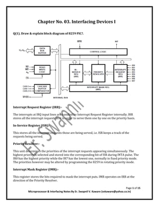
  • 1. Page 1 of 15 Microprocessor & Interfacing Notes By Er. Swapnil V. Kaware (svkaware@yahoo.co.in) Chapter No. 03. Interfacing Devices I Q(1). Draw & explain block diagram of 8259 PIC?. Interrupt Request Register (IRR):- The interrupts at IRQ input lines are handled by Interrupt Request Register internally. IRR stores all the interrupt requests in it in order to serve them one by one on the priority basis. In-Service Register (ISR):- This stores all the interrupt requests those are being served, i.e. ISR keeps a track of the requests being served. Priority Resolver:- This unit determines the priorities of the interrupt requests appearing simultaneously. The highest priority is selected and stored into the corresponding bit of ISR during INTA pulse. The IR0 has the highest priority while the IR7 has the lowest one, normally in fixed priority mode. The priorities however may be altered by programming the 8259 in rotating priority mode. Interrupt Mask Register (IMR):- This register stores the bits required to mask the interrupt puts. IMR operates on IRR at the direction of the Priority Resolver.
  • 2. Page 2 of 15 Microprocessor & Interfacing Notes By Er. Swapnil V. Kaware (svkaware@yahoo.co.in) Interrupt Control Logic:- This block manages the interrupt and interrupt acknowledge sigD8ls to be sent to the CPU for serving one of the eight interrupt requests. This also accepts interrupt acknowledge (INTA) signal from CPU that causes the 8259 to release vector address on to the data bus. Data Bus Buffer:- This tri-state bidirectional buffer interfaces internal 8259 bus to the microprocessor system data bus. Control words, status and vector information pass through buffer during read or write operations. Read write Control Logic:- This circuit accepts and decodes commands from the CPU. This also allows the status of the 8259 to be transferred on to the data bus. Cascade Buffer/Comparator:- The three I/O pins CAS0-2 are outputs when the 8259 is used as a master. The same pins act as inputs when the 8259 is in slave mode. The 8259 in master mode sends the ID of the interrupting slave device on these lines. The slave thus selected, will send its pre programmed vector address on the data bus during the next INTA pulse. CS:- This is an active-low chip select signal for enabling RD and WR operations of 8259. INTA function is independent of CS. WR:- This pin is an active-low write enable input to 8259. This enables it to accept command words from CPU. RD:- This is an active-low read enable input to 8259. A low on this line enables 8259 to release status onto the data bus of CPU. D7-D0 These pins form a bidirectional data bus that carries 8- bit data either to control word or from status word registers. CASo-CAS2:- Cascade Lines A single 8259 provides eight vectored interrupts. If more interrupts are required, the 8259 is used in cascade mode. In cascade mode, a master 8259 along with eight slaves 8259
  • 3. Page 3 of 15 Microprocessor & Interfacing Notes By Er. Swapnil V. Kaware (svkaware@yahoo.co.in) can provide up to 64 vectored interrupt lines. These three lines act as select lines for addressing the slaves 8259. SP/EN:- This pin is a dual purpose pin. When the chip is used in buffered mode, it can be used as buffer enable to control buffer trans-receivers. If this is not used in buffered mode then the pin is used as input to designate whether the chip is used as a master (SP = 1) or a slave (EN = 0). INT:- This pin goes high whenever a valid interrupt request is asserted. This is used to interrupt the CPU and is connected to the interrupt input of CPU. IR0-IR7 (Interrupt requests):- These pins act as inputs to accept interrupt requests to the CPU. In edge triggered mode, an interrupt service is requested by raising an IR pin from a low to a high state and holding it high until it is acknowledged, and just by latching it to high level, if used in level triggered mode. Q(2). Explain command words of 8259 PIC?. OR Q(3). Explain ICW1 and ICW3 in detail?. The command words of 8259 are classified in two groups, viz. initialization command words (ICWs) and operation command words (OCWs). Initialization Command Words (ICWs):- If A0 = 0 and D4 = 1, the control word is recognized as ICW1. It contains the control bits for edge/level triggered mode, single/cascade mode, call address interval and whether ICW4 is required or not, etc. If A0 = 1, the control word is recognized as ICW2. The ICW2 stores details regarding interrupt vector addresses. ICW1 and ICW2 are compulsory command words in initialization sequence of 8259 while ICW3 and ICW4 are optional. The ICW3 is read only when there are more than one 8259 in the system, i.e. cascading is used (SNGL = 0). The SNGL bit in ICW1 indicates whether the 8259 is in cascade mode or not. In master mode [i.e. SP = 1 or in buffer mode M/S = 1 in ICW4], the 8-bit slave register will be set bit-wise to '1' for each slave in the system. The requesting slave will then release the second byte of a CALL sequence. In slave mode [i.e. SP=0 or if BUF=1 and M/S=0 in ICW4] bits D2 to D0 identify the slave, i.e. 000 to 111 for slave 1 to slave 8. The slave compares the cascade inputs with these bits and if they are equal, the second byte if the CALL sequence is released by it on the data bus.
  • 4. Page 4 of 15 Microprocessor & Interfacing Notes By Er. Swapnil V. Kaware (svkaware@yahoo.co.in)
  • 5. Page 5 of 15 Microprocessor & Interfacing Notes By Er. Swapnil V. Kaware (svkaware@yahoo.co.in) The use of this command word depends on the IC4 bit of ICW1. If IC4= 1, ICW4 is used, otherwise it is neglected. The bit functions of ICW4 are described as follows: SFNM Special fully nested mode is selected, if SFNM = 1. (i). BUF If BUF = 1, the buffered mode is selected. In the buffered mode, (ii). SP/EN acts as enable output and the master/slave is determined using the M/S bit of ICW4. (iii). If M/S = 1, 8259 is a master. If M/S = 0, 8259 is a slave. If BUF =0, M/S is to be neglected. (iv). If AEOI = 1, the automatic end of interrupt mode is selected. (v). If ÎĽPM=0, the Mcs-85 system operation is selected and if ÎĽPM =1, 8086/88 operation is selected. Q(4). Explain operating modes of 8259 PIC?. The different modes of operation of 8259 can be programmed by setting or resting the appropriate bits of the ICWs or OCWs. The different modes of operation of 8259 are explained as, (i). Fully Nested Mode:- This is the default mode of operation of 8259. IR0 has the highest priority and IR7 has the lowest one. When interrupt requests are noticed, the highest priority request amongst them is determined and the vector is placed on the data bus. The corresponding bit of ISR is set and remains set till the microprocessor issues an EOI command just before returning from the service routine or the AEOI bit is set. If the ISR (in service) bit is set, all the same or lower priority interrupts are inhibited but higher levels will generate an interrupt, that will be acknowledged only if the microprocessor's interrupt enable flag (IF) is set. The priorities can afterwards be changed by programming the rotating priority modes. (ii). End of Interrupt (EOI):- The ISR bit can be reset either with AEOI bit of ICW1 or by EOI command, issued before returning from the interrupt service routine. There are two types of EOI commands specific and non-specific. When 8259 is operated in the modes that preserve fully nested structure, it can determine which ISR bit is to be reset on EOT. When nonspecific EOI command is issued to 8259 it will automatically reset the highest ISR bit out of those already set. When a mode that may disturb the fully nested structure is used, the 8259 is no longer able to determine the last level acknowledged. In this case a specific EOI command is issued to reset a particular ISR bit. An ISR bit that is masked by
  • 6. Page 6 of 15 Microprocessor & Interfacing Notes By Er. Swapnil V. Kaware (svkaware@yahoo.co.in) the corresponding IMR bit, will not be cleared by a non-specific EOI of 8259, if it is in special mask mode. (iii). Automatic Rotation:- This is used in the applications where all the interrupting devices are of equal priority. In this mode, an interrupt request (IR) level receives lowest priority after it is served while the next device to be served gets the highest priority in sequence. Once all the devices are served like this, the first device again receives highest priority. (iv). Automatic EOI Mode:- Till AEOI = 1 in ICW4, the 8259 operates in AEOI mode. In this mode, the 8259 performs a non- specific EOI operation at the trailing edge of the last INTA pulse automatically. This mode should be used only when a nested multilevel interrupt structure is not required with a single 8259. (v). Specific Rotation:- In this mode a bottom priority level can be selected, using L2, L1 and L0 in OCW2 and R =1, SL = 1, EOI = 0. The selected bottom priority fixes other priorities. If IR5 is selected as a bottom priority, then IR5 will have least priority and IR4 will have a next higher priority. Thus IR6 will have the highest priority. These priorities can be changed during an EOI command by programming the rotate on specific EOI command in OCW2 (vi). Special Mask Mode:- In special mask mode, when a mask bit is set in OCW1, it inhibits further interrupts at that level and enables interrupt from other levels, which are not masked. (vii). Edge and Level Triggered Mode:- This mode decides whether the interrupt should be edge triggered or level triggered. If bit LTIM of ICW1 = 0, they are edge triggered, otherwise the interrupts are level triggered. Reading 8259 Status The status of the internal registers of 8259 can be read using this mode. The OCW3 is used to read IRR and ISR while OCW1 is used to read IMR. Reading is possible only in no polled mode. (viii). Poll Command:- In polled mode of operation, the INT output of 8259 is neglected, though it functions normally, by not connecting INT output or by masking INT input of the microprocessor. The poll mode is entered by setting P =1 in OCW3. The 8259 is polled by using software execution by microprocessor instead of the requests on INT input. The 8259 treats the next RD pulse to the
  • 7. Page 7 of 15 Microprocessor & Interfacing Notes By Er. Swapnil V. Kaware (svkaware@yahoo.co.in) 8259 as an interrupt acknowledge. An appropriate ISR bit is set, if there is a request. The priority level is read and a data word is placed on to data bus, after RD is activated A poll command may give you more than 64 priority levels. Note that this has nothing to do with the 8086 interrupt structure and the interrupt priorities. (ix). Special Fully Nested Mode:- This mode is used in more complicated systems, where cascading is used and the priority has to be programmed in the master using ICW4. This is somewhat similar to the normal nested mode. In this mode, when an interrupt request from a certain lave is in service, this slave can further send requests to the master, if the requesting device connected to the slave has higher priority than the one being currently served. In this mode, the master interrupts the CPU only when the interrupting device has a higher or the same priority than the one currently being served. In normal mode, other requests than the one being served are masked out. When entering the interrupt service routine the software has to check whether this is the only request from the slave. This is done by sending a nonspecific EOI command to the slave and then reading its ISR and checking for zero. If its zero, a non-specific EOI can be sent to the master, otherwise no EOI should be sent. This mode is important, since in the absence of this mode, the slave would interrupt the master only once and hence the priorities of the 'lave inputs would have been disturbed. (x). Buffered Mode:- When the 8259 is used in the systems where bus driving buffers are used on data buses (e.g. cascade systems). The problem of enabling the buffers exists. The 8259 sends buffer enable signal on SP /EN pin, whenever data is placed on the bus. (xii). Cascade Mode The 8259 can be connected in a system containing one master and eight laves (maximum) to handle up to 64 priority levels. The master controls the slaves using CAS0-CAS2 which act as chip select inputs (encoded) for slaves. In this mode, the slave INT outputs are connected with master IR inputs. When a slave request line is activated and acknowledged, the master will enable the slave to release the vector address during second pulse of INTA sequence. The cascade lines are normally low and contain slave address codes from the trailing edge of the first INT A pulse to the trailing edge of the second INT A pulse. Each 8259 in the system must be separately initialized and programmed to work in different modes. The EOI command must be issued twice, one for master and the other for the slave. A separate address decoder is used to activate the chip select line of each 8259.
  • 8. Page 8 of 15 Microprocessor & Interfacing Notes By Er. Swapnil V. Kaware (svkaware@yahoo.co.in) Q(5). Draw & explain block diagram/architecture of 8251 USART?. The 8251 is a programmable chip designed for synchronous and asynchronous serial data communication. The INTEL 8251 is the industry standard Universal Synchronous Asynchronous Receiver Transmitter (USART) designed for data communications. The 8251 is used as a peripheral device and is programmed by the CPU to operate using virtually any serial data transmission technique. The USART accepts data characters from the CPU in parallel format and then converts them into a continuous serial data stream for transmission simultaneously; it can receive serial data streams and convert them into parallel data character for the CPU. The USART will signal the CPU whenever it can accept a new character for transmission or whenever it has received a character for the CPU. The block diagram includes five section, (i). Read/write Control Logic, (ii). Transmitter, (iii). Receiver, (iv). Modem Control, (v). Data Bus Buffer.
  • 9. Page 9 of 15 Microprocessor & Interfacing Notes By Er. Swapnil V. Kaware (svkaware@yahoo.co.in) (i). Read/Write Control Logic:- The control logic interfaces the chip with the processor, determines the functions of the chip according to the control word in its register, and monitors the data flow. (ii). Transmitter:- The transmitter section converts a parallel word received from the processor into serial bits and transmits them over the TxD line to a peripheral. (iii). Receiver:- The transmitter section receives serial bits from a peripheral, converts them into a parallel word, and transfers the word to the ÎĽP. (iv). Modem Control:- The modem control is used to establish data communication through modems over telephone lines. (v). Data Bus Buffer:- This bidirectional register can be addressed as an input and an output port when the pin is low. The function of various signals of 8251 USART is as given below, (a). D0 to D7 (l/O terminal):- This is bidirectional data bus which receive control words and transmits data from the CPU and sends status words and received data to CPU. (b). RESET (Input terminal):- A "High" on this input forces the 8251 into "reset status." The device waits for the writing of "mode instruction." The min. reset width is six clock inputs during the operating status of CLK. (c). CLK (Input terminal):- CLK signal is used to generate internal device timing. CLK signal is independent of RXC or TXC. However, the frequency of CLK must be greater than 30 times the RXC and TXC at Synchronous mode and Asynchronous "x1" mode, and must be greater than 5 times at Asynchronous "x16" and "x64" mode. (d). WR (Input terminal):- This is the "active low" input terminal which receives a signal for writing transmit data and control words from the CPU into the 8251.
  • 10. Page 10 of 15 Microprocessor & Interfacing Notes By Er. Swapnil V. Kaware (svkaware@yahoo.co.in) (e). RD (Input terminal):- This is the "active low" input terminal which receives a signal for reading receive data and status words from the 8251. (f). C/D (Input terminal):- This is an input terminal which receives a signal for selecting data or command words and status words when the 8251 is accessed by the CPU. If C/D = low, data will be accessed. If C/D = high, command word or status word will be accessed. (g). CS (Input terminal):- This is the "active low" input terminal which selects the 8251 at low level when the CPU accesses. Note: The device won’t be in "standby status"; only setting CS = High. (h). TXD (output terminal):- This is an output terminal for transmitting data from which serial-converted data is sent out. The device is in "mark status" (high level) after resetting or during a status when transmit is disabled. It is also possible to set the device in "break status" (low level) by a command. (i). TXRDY (output terminal):- This is an output terminal which indicates that the 8251is ready to accept a transmitted data character. But the terminal is always at low level if CTS = high or the device was set in "TX disable status" by a command. Note: TXRDY status word indicates that transmit data character is receivable, regardless of CTS or command. If the CPU writes a data character, TXRDY will be reset by the leading edge or WR signal. (j). TXEMPTY (Output terminal):- This is an output terminal which indicates that the 8251 has transmitted all the characters and had no data character. In "synchronous mode," the terminal is at high level, if transmit data characters are no longer remaining and sync characters are automatically transmitted. If the CPU writes a data character, TXEMPTY will be reset by the leading edge of WR signal. Note : As the transmitter is disabled by setting CTS "High" or command, data written before disable will be sent out. Then TXD and TXEMPTY will be "High". Even if a data is written after disable, that data is not sent out and TXE will be "High". After the transmitter is enabled, it sent out.
  • 11. Page 11 of 15 Microprocessor & Interfacing Notes By Er. Swapnil V. Kaware (svkaware@yahoo.co.in) (k). TXC (Input terminal):- This is a clock input signal which determines the transfer speed of transmitted data. In "synchronous mode," the baud rate will be the same as the frequency of TXC. In "asynchronous mode", it is possible to select the baud rate factor by mode instruction. It can be 1, 1/16 or 1/64 the TXC. The falling edge of TXC sifts the serial data out of the 8251. (l). RXD (input terminal):- This is a terminal which receives serial data. (m). RXRDY (Output terminal):- This is a terminal which indicates that the 8251 contains a character that is ready to READ. If the CPU reads a data character, RXRDY will be reset by the leading edge of RD signal. Unless the CPU reads a data character before the next one is received completely, the preceding data will be lost. In such a case, an overrun error flag status word will be set. (n). RXC (Input terminal):- This is a clock input signal which determines the transfer speed of received data. In "synchronous mode," the baud rate is the same as the frequency of RXC. In "asynchronous mode," it is possible to select the baud rate factor by mode instruction. It can be 1, 1/16, 1/64 the RXC. (o). SYNDET/BD (Input or output terminal):- This is a terminal whose function changes according to mode. In "internal synchronous mode." this terminal is at high level, if sync characters are received and synchronized. If a status word is read, the terminal will be reset. In "external synchronous mode, "this is an input terminal. A "High" on this input forces the 8251 to start receiving data characters. In "asynchronous mode," this is an output terminal which generates "high level" output upon the detection of a "break" character if receiver data contains a "low-level" space between the stop bits of two continuous characters. The terminal will be reset, if RXD is at high level. After Reset is active, the terminal will be output at low level. (p). DSR (Input terminal):- This is an input port for MODEM interface. The input status of the terminal can be recognized by the CPU reading status words. (q). DTR (Output terminal):- This is an output port for MODEM interface. It is possible to set the status of DTR by a command.
  • 12. Page 12 of 15 Microprocessor & Interfacing Notes By Er. Swapnil V. Kaware (svkaware@yahoo.co.in) (r). CTS (Input terminal):- This is an input terminal for MODEM interface which is used for controlling a transmit circuit. The terminal controls data transmission if the device is set in "TX Enable" status by a command. Data is transmittable if the terminal is at low level. (s). RTS (Output terminal):- This is an output port for MODEM interface. It is possible to set the status RTS by a command. Q(6). Draw & explain mode register format for USART 8251 for synchronous and asynchronous mode. There are two types of control word, 1. Mode instruction (setting of function) & 2. Command (setting of operation) 1) Mode Instruction:-
  • 13. Page 13 of 15 Microprocessor & Interfacing Notes By Er. Swapnil V. Kaware (svkaware@yahoo.co.in) Mode instruction is used for setting the function of the 8251. Mode instruction will be in "wait for write" at either internal reset or external reset. That is, the writing of a control word after resetting will be recognized as a "mode instruction." In the case of synchronous mode, it is necessary to write one-or two byte sync characters. If sync characters were written, a function will be set because the writing of sync characters constitutes part of mode instruction. 2) Command:- Command is used for setting the operation of the 8251. It is possible to write a command whenever necessary after writing a mode instruction and sync characters.
  • 14. Page 14 of 15 Microprocessor & Interfacing Notes By Er. Swapnil V. Kaware (svkaware@yahoo.co.in) Status Word:- It is possible to see the internal status of the 8251 by reading a status word. The bit configuration of status word is shown in Figure..
  • 15. Page 15 of 15 Microprocessor & Interfacing Notes By Er. Swapnil V. Kaware (svkaware@yahoo.co.in) ***************************************** ALL THE BEST *****************************************