SlideShare a Scribd company logo
1 of 57
PROGRAMMABLE PERIPHERAL
INTERFACE -8255
Features:
• It is a programmable device.
• It has 24 I/O programmable pins like PA,PB,PC (3-8
pins).
 T T L compatible.
 Improved dc driving capability
Pin Diagram
Function of pins:
• Data bus(D0-D7):These are 8-bit bi-directional buses,
connected to 8085 data bus for transferring data.
• CS: This is Active Low signal. When it is low, then
data is transfer from 8085.
• Read: This is Active Low signal, when it is Low read
operation will be start.
• Write: This is Active Low signal, when it is Low Write
operation will be start.
A1 A0 Select
0 0 PA
0 1 PB
1 0 PC
1 1
Control
reg.
• Address (A0-A1):This is used to select the
ports. like this
• RESET: This is used to reset the device. That means
clear control registers.
• PA0-PA7:It is the 8-bit bi-directional I/O pins used to
send the data to peripheral or
or to receive the data from peripheral.
• PB0-PB7:Similar to PA
• PC0-PC7:This is also 8-bit bidirectional I/O pins.
These lines are divided into two groups.
1. PC0 to PC3(Lower Groups)
2. PC4 to PC7 (Higher groups)
These two groups working in separately using 4
data’s.
Block Diagram
Data Bus buffer:
• It is a 8-bit bidirectional Data bus.
• Used to interface between 8255 data bus with
system bus.
• The internal data bus and Outer pins D0-D7
pins are connected in internally.
• The direction of data buffer is decided by
Read/Control Logic.
Read/Write Control Logic:
• This is getting the input signals from control
bus and Address bus
• Control signal are RD and WR.
• Address signals are A0,A1,and CS.
• 8255 operation is enabled or disabled by CS.
Group A and Group B control:
• Group A and B get the Control
Signal from CPU and send the command to the individual
control blocks.
• Group A send the control signal to port A and Port C
(Upper) PC7-PC4.
• Group B send the control signal to port B and Port C
(Lower) PC3-PC0.
PORT A:
• This is a 8-bit buffered I/O latch.
• It can be programmed by mode 0 , mode 1, mode 2 .
PORT B:
• This is a 8-bit buffer I/O latch.
• It can be programmed by mode 0 and mode 1.
PORT C:
• This is a 8-bit Unlatched buffer Input and an
Output latch.
• It is splitted into two parts.
• It can be programmed by bit set/reset operation.
Operation modes:
BIT SET/RESET MODE:
• The PORT C can be Set or Reset by sending OUT
instruction to the CONTROL registers.
I/O MODES:
• MODE 0(Simple input / Output):
• In this mode , port A, port B and port C is used as
individually (Simply).
• Features:
• Outputs are latched , Inputs are buffered not latched.
• Ports do not have Handshake or interrupt capability.
MODE 1 :(Input/output with Hand shake)
• In this mode, input or output is transferred by
hand shaking Signals.
• Handshaking signals is used to transfer data
between whose data transfer is not same.
Computer Printer
DATA BUS
STB
ACK
Busy
Example:
• The computer send the data to the printer large
speed compared to the printer.
• When computer send the data according to the
printer speed at the time only, printer can accept.
• If printer is not ready to accept the data then after
sending the data bus , computer uses another
handshaking signal to tell printer that valid data is
available on the data bus.
• Each port uses three lines from port C as
handshake signals
MODE 2:Bi-directional I/O data transfer:
• This mode allows bidirectional data transfer over
a single 8-bit data bus using handshake signals.
• This feature is possible only Group A
• Port A is working as 8-biy bidirectional.
• PC3-PC7 is used for handshaking purpose.
• The data is sent by CPU through this port , when
the peripheral request it.
CONTROL WORD FORMATS:
• In the INPUT mode , When RESET is High all 24
pins (3-ports) be a input mode.
• i.e all flip flops are cleared and the interrupts are
rest.
• This condition is maintained even after RESET
goes low.
• This can be avoid by writing single control word to
the control registers , when required.
Control Word Format of 8255
FOR BIT SET/RESET MODE:
• This is bit set/reset control word format.
X X X
Don’t care
Bit select
B0
B1
B2
D7 D6 D5 D4 D3 D2 D1 D0
0 1 2 3 4 5 6 7
0 1 0 1 0 1 0 1
0 0 1 1 0 0 1 1
0 0 0 0 1 1 1 1
BIT SET/RESET
1=SET
0=RESET
BIT SET/RESET FLAG
=0 Active
• PC0-PC7 is set or reset as per the status of D0.
• A BSR word is written for each bit
• Example:
• PC3 is Set then control register will be 0XXX0111.
• PC4 is Reset then control register will be
0XXX01000.
• X is a don’t care.
• FOR I/O MODE:
The mode format for I/O as shown in figure
D7 D6 D5 D4 D3 D2 D1 D0
Group A
Port C Upper
1=Input
0=Output
Port B
1=Input
0=Output
Mode selection
00=mode 0
01=mode 1
1x=mode 2
Group B
Port C Lower
1=Input
0=Output
Port B
1=Input
0=Output
Mode selection
0=mode 0
1=mode 1
Mode set
flag=1=Active
• The control word for both mode is same.
• Bit D7 is used for specifying whether word
loaded in to Bit set/reset mode or Mode
definition word.
• D7=1=Mode definition mode.
• D7=0=Bit set/Reset mode.
8254 Prgrammable Interval Timer
Features of 8254 Prgrammable Interval Timer
Three independent 16 bit down counters.
Counters can be programmed in 6 different programmable counter modes.
Counting facility in both binary or BCD number system.
Compatible with Intel and other microprocessor.
Single +5 V supply.
24 Pin dual in-line package.
Pin Configuration of 8254 PIT
Pin description of 8254 PIT
Architecture of 8254 PIT
This device is useful whenever the microprocessor must control real-time events.
The timer in a personal computer is an 8254. To operate a counter a 16-bit count is loaded
in its register and on command, it begins to decrement the count until it reaches 0. At the
end of the count it generates a pulse, which interrupts the processor.
The count can count either in binary or BCD Each counter in the block diagram has 3
logical lines connected to it. Two of these lines, clock and gate, are inputs. The third, labeled
OUT is an output.
Data bus buffer- It is a communication path between the timer and the microprocessor.
The buffer is 8-bit and bidirectional. It is connected to the data bus of the microprocessor.
Read /write logic controls the reading and the writing of the counter registers. Control word
register, specifies the counter to be used and either a Read or a write operation. Data is
transmitted or received by the buffer upon execution of INPUT instruction from CPU.
The data bus buffer has three basic functions,
Programming the modes of 8254.
Loading the count value in timers
Reading the count value from timers
The data bus buffer is connected to microprocessor using D7 – D0 pins which are also
bidirectional. The data transfer is through these pins. These pins will be in high- impedance
(or this state) condition until the 8254 is selected by a LOW or CS and either the read
operation requested by a LOW RD on the input or a write operation WR requested by the
input going LOW.
Read/ Write Logic: It accepts inputs for the system control bus and in turn generation the control
signals for overall device operation. It is enabled or disabled by CS so that no operation can occur
to change the function unless the device has been selected as the system logic.
CS : The chip select input is used to enable the communicate between 8254 and the
microprocessor by means of data bus. A low an CS enables the data bus buffers, while a high
disable the buffer. The CS input does not have any affect on the operation of three times once they
have been initialized. The normal configuration of a system employs an decode logic which actives
CS line, whenever a specific set of addresses that correspond to 8254 appear on the address bus.
RD & WR :The read ( RD ) and write WR pins central the direction of data transfer on the 8-bit bus.
When the input RD pin is low. Then CPU is inputting data from 8254 in the form of counter value.
When WR pins is low, then CPU is sending data to 8254 in the form of mode information or loading
counters. The RD &WR should not both be low simultaneously. When RD & WR pins are HIGH, the
data bus buffer is disabled.
A0 & A1:These two input lines allow the microprocessor to specify which one of the internal
register in the 8254 is going to be used for the data transfer. Fig shows how these two lines are used
to select either the control word register or one of the 16-bit counters.
A1 A0 Function
0 0 Counter 0
0 1 Counter 1
1 0 Counter 2
1 1 Control Word
Control word register: It is selected when A0 and A1 . It the accepts information from the
data bus buffer and stores it in a register. The information stored in then register controls the
operation mode of each counter, selection of binary or BCD counting and the loading of each
counting and the loading of each count register. This register can be written into, no read
operation of this content is available.
Counters: Each of the times has three pins associated with it. These are CLK (CLK) the gate
(GATE) and the output (OUT).
CLK: This clock input pin provides 16-bit times with the signal to causes the times to
decrement maximum clock input is 2.6MHz. Note that the counters operate at the negative
edge (H1 to L0) of this clock input. If the signal on this pin is generated by a fixed oscillator
then the user has implemented a standard timer. If the input signal is a string of randomly
occurring pulses, then it is called implementation of a counter.
GATE: The gate input pin is used to initiate or enable counting. The exact effect of the gate
signal Depends on which of the six modes of operation is chosen.
OUTPUT: The output pin provides an output from the timer. It actual use depends on the
mode of Operation of the timer. The counter can be read ―in the fly‖ without inhibiting gate
pulse or clock input.
Control word register Format of 8254
Modes Of Operation
•Mode 0: Interrupt On Terminal Count,
•Mode 1: Programmable One Shot,
•Mode 2: Rate Generator ,
•Mode 3: Square Wave Rate Generator
•Mode 4: Software Triggered Strobe
•Mode 5: Hardware Triggered Strobe
Programmable Interrupt Controller-8259
Features of The 8259
 8259 is a programmable interrupt controller specially designed
to work with Intel microprocessor 8080, 8085A, 8086, 8088.
 It can handle eight interrupt inputs. This is equivalent to
providing eight interrupt pins on the processor in place of one
INTR (in 8085A)/INT(in 8086) pin.
 It can resolve eight levels of interrupt priorities in a variety of
modes. The priorities of interrupts can be changed under running
condition. Some of the desired lower priority interrupts may be
allowed to be acknowledged during the service of higher priority
interrupts.
 Each of the interrupt requests can be masked individually similar to RST7.5,
RST6.5 and RST5.5 interrupts of 8085A.
 The status of pending interrupts, in service interrupts,and masked interrupts
can be read at any time similar to RST interrupts of 8085A.
 The chip can be programmed to accept interrupt requests either as level
triggered or edge triggered interrupt request unlike your RST interrupts
where some are edge triggered and some are level triggered. However, all
interrupts must be either level triggered or edge triggered.
 If required, nine 8259As can be cascaded in a master-slave configuration
mode to handle 64 interrupt inputs. In this case, the interrupting devices send
their interrupt requests either to slave 8259A or to master 8259A directly.
The slave 8259As send their interrupt to master interrupt request inputs and
the master will send a single interrupt to microprocessor interrupt pin
Pin Configuration of Intel 8259A
• The 8259 A is contained in a 28 dual-in-line package that requires only
+5V supply voltage. The 8259A is upward compatible with 8259. The main
difference between the two is that the 8259A can be used with Intel
8086/8088 processor. It also includes additional features such as level
triggered mode, buffered mode and automatic end of interrupt mode.
• The pin diagram and internal block diagram of PIC is shown in figure. The
pins are defined as follows:
 CS (Chip Select signal): To access this chip, chip select signal CS is made
low. A LOW on this pin enables RD & WR communication between the
CPU and the 8259A. This signal is made LOW by decoding the addresses
assigned to this chip. Therefore, this pin is connected to address bus
through the decoder logic circuit. Interrupt acknowledge functions to
transfer the control to interrupt service subroutine are independent of CS .
 WR (Write signal): A low on this pin. When CS is low enables the
8259 A to accept command words from CPU.
 RD (Read signal): A low on this pin when CS is low enables this
8259A to release status (pending interrupts or in-service interrupts or
masked interrupts) on to the data bus for the CPU. The status includes
the contents of IMR (interrupt mask register) or ISR(interrupt service
register) or IRR (interrupt request register) or a priority level.
 D7-D0 (Data Bus): Bidirectional data bus. Control, status and
interrupt vector information is transferred via this data bus. This bus
is connected to BDB of 8085A. CAS2-CAS0 (Cascade lines): The
CAS2-0 lines form a local 8259A bus to control multiple 8259As in
master-slave configuration, i.e., to identify a particular slave 8259A to
be accessed for transfer of vector information. These pins are
automatically set as output pins for master 8259A and input pins for a
slave 8259A once the chips are programmed as master or slave.
 SP / EN (Salve Program/Enable Buffer): This is a dual function pin.
When the chip is programmed in buffered mode, the pin can be used
as an output and when not in the buffered mode it is used as an
input. In non-buffered mode it is used as an input pin to determine
whether the 8259A is to be used as a master (SP / EN = 1) or as a
slave (SP / EN = 0). In buffered mode, normally data bus buffers are
used. These buffers need to be enabled or disabled during transfer of
vector information depending upon whether 80259A is connected
before the buffer or after the buffer. To disable/enable the data bus
transceivers (buffers) when data are being transferred from the
8259A to the CPU, this pin is made low or high.
 INT (Interrupt output): This pin goes high whenever a valid
interrupt request is asserted. It is used to interrupt the CPU, thus it is
connected to the CPU’s interrupt pin (INTR). In case of master-slave
configuration, the interrupt pin of slave 8259A is connected to
interrupt request input of master 8259A.
INTA (Interrupt Acknowledge): This pin is used to enable 8259A
interrupt vector data on the data bus by a sequence of interrupt
acknowledge pulses issued by the CPU.
IR0-IR7 (Interrupt Request inputs): These are asynchronous interrupt
request input pins. An interrupt request is executed by raising an IR input
(low to high), and holding it high until it is acknowledged. (Edge
triggered mode) or just by a high level on an interrupt request input (Level
triggered mode).
A0 (A0 address line): This pin acts in conjunction with the RD , WR
&CS pins. It is used by the 8259A to send various command words from
the CPU and to read the status. It is normally connected to the CPU A0
address line. Two addresses are assigned/ reserved in the I/O address
space for each 8259A in the system- one with A0 =0 is called even address
and other with A0 = 1 is called odd address.
Internal Structure of 8259A
Functional Description of 8259:
 The 8259A (PIC) has eight interrupt request inputs – IR7 -IR0.The
8259A uses its INT output to interrupt the 8086 via INTR pin. The
8259A receives interrupt acknowledge pulses from the 𝜇𝑝 at its
INTA input. Vector address, used by the 8086 to transfer control to
the service subroutine of the interrupting device, is provided by the
8259A on the data bus. The 8259A is a programmable device that
must be initialized by command words sent by the microprocessor.
After initialization the 8259A mode of operation can be changed by
operation command words from the microprocessor
Data bus buffer: This 3- state, bidirectional 8-bit buffer is used to
interface the 8259A to the system data bus. Control words and status
information from the microprocessor to PIC and from PIC to
microprocessor respectively, are transferred through the data bus buffer.
Read/Write & Control Logic: The function of this block is to accept
output commands sent from the CPU. It contains the initialization
command word (ICW) registers and operation command word (OCW)
registers which store the various control formats for device operation.
This function block also allows the status of 8259A to be transferred to
the data bus.
Interrupt Request Register (IRR): Interrupt request register (IRR) stores
all the interrupt inputs that are requesting service. It is an 8-bit register –
one bit for each interrupt request. Basically, it keeps track of which
interrupt inputs are asking for service. If an interrupt input is unmasked,
and has an interrupt signal on it, then the corresponding bit in the IRR
will be set. The content of this register can be read to know the status of
pending interrupts.
Interrupt Mask Register (IMR): The IMR is used to disable (Mask)or enable
(Unmask) individual interrupt request inputs. This is also an 8-bit register. Each bit
in this register corresponds to the interrupt input with the same number. The IMR
operates on the IRR. Masking of higher priority input will not affect the interrupt
request lines of lower priority. To unmask any interrupt the corresponding bit is set
‘0’.
In-service Register (ISR): The in-service register keeps track of which interrupt
inputs are currently being serviced. For each input that is currently being serviced
the corresponding bit of in-service register (ISR) will be set. In 8259A, during the
service of an interrupt request, if another higher priority interrupt becomes active, it
will be acknowledged and the control will be transferred from lower priority
interrupt service subroutine (ISS) to higher priority ISS. Thus, more than one bit of
ISR will be set indicating the number of interrupts being serviced.
Each of these 3-registers can be read as status register.
Priority Resolver: This logic block determines the priorities of the interrupts
set in the IRR. It takes the information from IRR, IMR and ISR to determine
whether the new interrupt request is having highest priority or not. If the new
interrupt request is having the highest priority, it is selected and processed. The
corresponding bit of ISR will be set during interrupt acknowledge machine
cycle.
Cascade Buffer/Comparator: This function block stores and compares the IDs of
all 8259A’s in the system. The associated 3-I/O lines (CAS2-CAS0) are outputs when
8259A is used as a master and are inputs when 8259A is used as a slave. As a master,
the 8259A sends the ID of the interrupting slave device onto the CAS2- CAS0 lines.
The slave 8259As compare this ID with their own programmed ID. Thus selected
8259A will send its pre-programmed subroutine address on to the data bus during the
next one or two successive INTA pulses.
• For master 8259 these pins are outputs and for slaves these are
inputs.
• When 8259 is a master the CALL op-code is generated by master
in response to the first Interrupt acknowledge.
• The vectoring address must be released by slave 8259
• The master puts out the identification code to select one of the
slave from 8 slaves through these pins.
• The slave accepts these three signals as inputs and compare the
code put out by the master with the codes assigned to them
during initialization.
• The slave thus selected puts out the address of ISR during second
and third interrupt acknowledge pulses from the CPU.
Slave Program/ Enable Buffer: SP/EN
• Used to specify whether 8259 is to act as a master or a slave
 High-Master
 Low – Slave
• In Non-Buffered Mode, this pin is used to specify whether 8259
is to act as a master or a slave.
• In Buffered mode this pin is used as an output to enable the data
bus buffer of the system.
8259APIC- Interrupt Operation
• To implement interrupt, the interrupt Enable FF must be enabled
by writing EI instruction.
• 8259A- should be initialized by writing control words in the
control register.
• 8259 requires two types of control words:
ICW- Used to set up proper conditions
 And specify RST vector address.
OCW- Used to perform functions such as
 Masking interrupts, setting up status
 Read operations etc.
After 8259A is initialized, the following sequence of events
occurs when one or more interrupt request lines go high.
1. IRR stores the Interrupt requests.
2. Priority Resolver Checks three registers: IRR-for interrupt requests.
IMR- for Masking bits. ISR- for the interrupt request being serviced. It
resolves the priority and sets the INT high when appropriate.
3. MPU acknowledges the interrupt by sending interrupt acknowledge.
4. After INTA is received, the appropriate priority bit in the ISR is set to
indicate which level is being served and the corresponding bit in the
IRR is reset to that request is accepted. Then op-code for CALL
instruction is placed on the Data Bus.
5. When MPU decodes the CALL instruction, it places two more signals
on the data bus.
6. When 8259 receives second INTA , it places lower order byte of CALL
address on the data bus. Third INTA High order byte. The CALL
address is the vector memory location for the interrupt. This address is
placed in control register during Initialization.
• During third INTA pulse, the ISR bit is reset either
automatically (AEOI) or by a command word that must be
issued at the end of the service routine (EOI). This option is
determined by the ICW.
8. The program sequence is transferred to thememory location
specified by the CALL Instruction.
 AEOI - Automatic End of Interrupt Mode
 EOI - End of Interrupt Mode
8259 System bus interface
8259A PIC- COMMAND WORDS
• Two types: ICW, OCW
ICW:
• Before start functioning, 8259 must be initialized by writing two to
four command words into their respective command word
registers.
• A0=0,D4=1: The control word is ICW1.ICW1-contains the control
bits for edge/level triggered mode, single/cascade mode, call
address interval and whether ICW4 is required or not etc.
• A0=1: ICW2- Store details interrupt vector addresses.
8259A PIC- ICW1
 The following initialization procedure Carried out internally
when ICW1is loaded.
1. The edge sense circuit is reset i.e. by default 8259A interrupts
are edge sensitive.
2. IMR is cleared.
3. IR7 input is assigned lowest priority.
4. Slave mode address is set to 7.
5. Special mask mode is cleared and status read is set to IRR.
6. If IC4=0, all functions of ICW4 are set to Zero. Master/slave
bit in ICW4 bit is used in buffered mode only
Initialization Sequence f 8259a
ICW1:
ICW2:
ICW3:
ICW4:
Operation Command Word 1 (OCW 1):
• A Write command to the 8259 with A0 = 1 (after ICW2) is
interpreted as OCW1. OCW1 is used for enabling or disabling the
recognition of specific interrupt requests by programming the IMR.
• M = 1 indicates that the interrupt is to be masked, and M = 0
indicates that it is to be unmasked
Operation Command Word 2 (OCW2):
• A Write command with A0 = 1 and D4 D3 = 00 is interpreted as OCW2.
The R (Rotate), SL (Select-Level), EOI bits control the Rotate and End
Of Interrupt Modes and combinations of the two.
• Figure shows the Operation Command Word format. L2-L0 are used to
specify the interrupt level to be acted upon when the SL bit is active.
Operation Command Word 2 (OCW2):
• When the ESMM (Enable special mask mode ) bit is set, then the SMM
bit is don’t care. If SMM = 1 and ESMM = 1, then 8259 will enter in
Special mask mode.
• If ESMM = 1 and SMM = 0, then 8259 will return into normal mask
mode.
• RR and RIS are used to give the read register command.
• P = 1 is used for poll command.

More Related Content

Similar to 8255-PPI MPMC text book for engineering.ppt

UNIT- 3.pptx
UNIT- 3.pptxUNIT- 3.pptx
UNIT- 3.pptxBASKARS53
 
UNIT 3 Peripheral Interfacing.pptx
UNIT 3 Peripheral Interfacing.pptxUNIT 3 Peripheral Interfacing.pptx
UNIT 3 Peripheral Interfacing.pptxGowrishankar C
 
8255 presentaion.ppt
8255 presentaion.ppt8255 presentaion.ppt
8255 presentaion.pptkamlesh deshmukh
 
Programmable Peripheral Devices
Programmable Peripheral Devices Programmable Peripheral Devices
Programmable Peripheral Devices glorypriyadharshini1
 
unit-3-8255.pdf
unit-3-8255.pdfunit-3-8255.pdf
unit-3-8255.pdfShanmukhSaiR
 
8255 ppi.pptx
8255 ppi.pptx8255 ppi.pptx
8255 ppi.pptxzahid235639
 
8251 a usart programmable communication interface(1)
8251 a usart   programmable communication interface(1)8251 a usart   programmable communication interface(1)
8251 a usart programmable communication interface(1)divyangpit
 
8255 ppi
8255 ppi8255 ppi
8255 ppiSuraj Bora
 
8251 universal synchronous asynchronous receiver transmitter
8251 universal synchronous asynchronous receiver transmitter8251 universal synchronous asynchronous receiver transmitter
8251 universal synchronous asynchronous receiver transmitterShivangiSharma879191
 
363118864 8255-nptel
363118864 8255-nptel363118864 8255-nptel
363118864 8255-nptelZerihunDemere
 
8255 class
8255 class8255 class
8255 classriyasekaran
 
chapter-4-microprocessor-interfacing.pptx
chapter-4-microprocessor-interfacing.pptxchapter-4-microprocessor-interfacing.pptx
chapter-4-microprocessor-interfacing.pptxJaypeeFajanil
 
Microprocessor Architecture-III
Microprocessor Architecture-IIIMicroprocessor Architecture-III
Microprocessor Architecture-IIIDr.YNM
 
Unit 3-1 (1)
Unit 3-1 (1)Unit 3-1 (1)
Unit 3-1 (1)Vasu Ch
 
Programmable peripheral interface 8255
Programmable peripheral interface 8255Programmable peripheral interface 8255
Programmable peripheral interface 8255Marajulislam3
 
8251 communication interface
8251 communication interface8251 communication interface
8251 communication interfaceLingalaSowjanya
 

Similar to 8255-PPI MPMC text book for engineering.ppt (20)

UNIT- 3.pptx
UNIT- 3.pptxUNIT- 3.pptx
UNIT- 3.pptx
 
UNIT 3 Peripheral Interfacing.pptx
UNIT 3 Peripheral Interfacing.pptxUNIT 3 Peripheral Interfacing.pptx
UNIT 3 Peripheral Interfacing.pptx
 
8255 presentaion.ppt
8255 presentaion.ppt8255 presentaion.ppt
8255 presentaion.ppt
 
Programmable Peripheral Devices
Programmable Peripheral Devices Programmable Peripheral Devices
Programmable Peripheral Devices
 
unit-3-8255.pdf
unit-3-8255.pdfunit-3-8255.pdf
unit-3-8255.pdf
 
Chapter5
Chapter5Chapter5
Chapter5
 
8255 ppi.pptx
8255 ppi.pptx8255 ppi.pptx
8255 ppi.pptx
 
8251 a usart programmable communication interface(1)
8251 a usart   programmable communication interface(1)8251 a usart   programmable communication interface(1)
8251 a usart programmable communication interface(1)
 
8255 ppi
8255 ppi8255 ppi
8255 ppi
 
8251 universal synchronous asynchronous receiver transmitter
8251 universal synchronous asynchronous receiver transmitter8251 universal synchronous asynchronous receiver transmitter
8251 universal synchronous asynchronous receiver transmitter
 
363118864 8255-nptel
363118864 8255-nptel363118864 8255-nptel
363118864 8255-nptel
 
L4-L6 8255 A.pptx
L4-L6 8255 A.pptxL4-L6 8255 A.pptx
L4-L6 8255 A.pptx
 
8255 class
8255 class8255 class
8255 class
 
1.ppi 8255
1.ppi 8255 1.ppi 8255
1.ppi 8255
 
MPMC
MPMC MPMC
MPMC
 
chapter-4-microprocessor-interfacing.pptx
chapter-4-microprocessor-interfacing.pptxchapter-4-microprocessor-interfacing.pptx
chapter-4-microprocessor-interfacing.pptx
 
Microprocessor Architecture-III
Microprocessor Architecture-IIIMicroprocessor Architecture-III
Microprocessor Architecture-III
 
Unit 3-1 (1)
Unit 3-1 (1)Unit 3-1 (1)
Unit 3-1 (1)
 
Programmable peripheral interface 8255
Programmable peripheral interface 8255Programmable peripheral interface 8255
Programmable peripheral interface 8255
 
8251 communication interface
8251 communication interface8251 communication interface
8251 communication interface
 

Recently uploaded

Introduction-To-Agricultural-Surveillance-Rover.pptx
Introduction-To-Agricultural-Surveillance-Rover.pptxIntroduction-To-Agricultural-Surveillance-Rover.pptx
Introduction-To-Agricultural-Surveillance-Rover.pptxk795866
 
DATA ANALYTICS PPT definition usage example
DATA ANALYTICS PPT definition usage exampleDATA ANALYTICS PPT definition usage example
DATA ANALYTICS PPT definition usage examplePragyanshuParadkar1
 
VICTOR MAESTRE RAMIREZ - Planetary Defender on NASA's Double Asteroid Redirec...
VICTOR MAESTRE RAMIREZ - Planetary Defender on NASA's Double Asteroid Redirec...VICTOR MAESTRE RAMIREZ - Planetary Defender on NASA's Double Asteroid Redirec...
VICTOR MAESTRE RAMIREZ - Planetary Defender on NASA's Double Asteroid Redirec...VICTOR MAESTRE RAMIREZ
 
What are the advantages and disadvantages of membrane structures.pptx
What are the advantages and disadvantages of membrane structures.pptxWhat are the advantages and disadvantages of membrane structures.pptx
What are the advantages and disadvantages of membrane structures.pptxwendy cai
 
Internship report on mechanical engineering
Internship report on mechanical engineeringInternship report on mechanical engineering
Internship report on mechanical engineeringmalavadedarshan25
 
Arduino_CSE ece ppt for working and principal of arduino.ppt
Arduino_CSE ece ppt for working and principal of arduino.pptArduino_CSE ece ppt for working and principal of arduino.ppt
Arduino_CSE ece ppt for working and principal of arduino.pptSAURABHKUMAR892774
 
Work Experience-Dalton Park.pptxfvvvvvvv
Work Experience-Dalton Park.pptxfvvvvvvvWork Experience-Dalton Park.pptxfvvvvvvv
Work Experience-Dalton Park.pptxfvvvvvvvLewisJB
 
GDSC ASEB Gen AI study jams presentation
GDSC ASEB Gen AI study jams presentationGDSC ASEB Gen AI study jams presentation
GDSC ASEB Gen AI study jams presentationGDSCAESB
 
CCS355 Neural Network & Deep Learning UNIT III notes and Question bank .pdf
CCS355 Neural Network & Deep Learning UNIT III notes and Question bank .pdfCCS355 Neural Network & Deep Learning UNIT III notes and Question bank .pdf
CCS355 Neural Network & Deep Learning UNIT III notes and Question bank .pdfAsst.prof M.Gokilavani
 
Software and Systems Engineering Standards: Verification and Validation of Sy...
Software and Systems Engineering Standards: Verification and Validation of Sy...Software and Systems Engineering Standards: Verification and Validation of Sy...
Software and Systems Engineering Standards: Verification and Validation of Sy...VICTOR MAESTRE RAMIREZ
 
Artificial-Intelligence-in-Electronics (K).pptx
Artificial-Intelligence-in-Electronics (K).pptxArtificial-Intelligence-in-Electronics (K).pptx
Artificial-Intelligence-in-Electronics (K).pptxbritheesh05
 
Architect Hassan Khalil Portfolio for 2024
Architect Hassan Khalil Portfolio for 2024Architect Hassan Khalil Portfolio for 2024
Architect Hassan Khalil Portfolio for 2024hassan khalil
 
Heart Disease Prediction using machine learning.pptx
Heart Disease Prediction using machine learning.pptxHeart Disease Prediction using machine learning.pptx
Heart Disease Prediction using machine learning.pptxPoojaBan
 
Concrete Mix Design - IS 10262-2019 - .pptx
Concrete Mix Design - IS 10262-2019 - .pptxConcrete Mix Design - IS 10262-2019 - .pptx
Concrete Mix Design - IS 10262-2019 - .pptxKartikeyaDwivedi3
 
main PPT.pptx of girls hostel security using rfid
main PPT.pptx of girls hostel security using rfidmain PPT.pptx of girls hostel security using rfid
main PPT.pptx of girls hostel security using rfidNikhilNagaraju
 
Call Us ≽ 8377877756 ≼ Call Girls In Shastri Nagar (Delhi)
Call Us ≽ 8377877756 ≼ Call Girls In Shastri Nagar (Delhi)Call Us ≽ 8377877756 ≼ Call Girls In Shastri Nagar (Delhi)
Call Us ≽ 8377877756 ≼ Call Girls In Shastri Nagar (Delhi)dollysharma2066
 

Recently uploaded (20)

Introduction-To-Agricultural-Surveillance-Rover.pptx
Introduction-To-Agricultural-Surveillance-Rover.pptxIntroduction-To-Agricultural-Surveillance-Rover.pptx
Introduction-To-Agricultural-Surveillance-Rover.pptx
 
DATA ANALYTICS PPT definition usage example
DATA ANALYTICS PPT definition usage exampleDATA ANALYTICS PPT definition usage example
DATA ANALYTICS PPT definition usage example
 
VICTOR MAESTRE RAMIREZ - Planetary Defender on NASA's Double Asteroid Redirec...
VICTOR MAESTRE RAMIREZ - Planetary Defender on NASA's Double Asteroid Redirec...VICTOR MAESTRE RAMIREZ - Planetary Defender on NASA's Double Asteroid Redirec...
VICTOR MAESTRE RAMIREZ - Planetary Defender on NASA's Double Asteroid Redirec...
 
Design and analysis of solar grass cutter.pdf
Design and analysis of solar grass cutter.pdfDesign and analysis of solar grass cutter.pdf
Design and analysis of solar grass cutter.pdf
 
What are the advantages and disadvantages of membrane structures.pptx
What are the advantages and disadvantages of membrane structures.pptxWhat are the advantages and disadvantages of membrane structures.pptx
What are the advantages and disadvantages of membrane structures.pptx
 
Internship report on mechanical engineering
Internship report on mechanical engineeringInternship report on mechanical engineering
Internship report on mechanical engineering
 
Arduino_CSE ece ppt for working and principal of arduino.ppt
Arduino_CSE ece ppt for working and principal of arduino.pptArduino_CSE ece ppt for working and principal of arduino.ppt
Arduino_CSE ece ppt for working and principal of arduino.ppt
 
Work Experience-Dalton Park.pptxfvvvvvvv
Work Experience-Dalton Park.pptxfvvvvvvvWork Experience-Dalton Park.pptxfvvvvvvv
Work Experience-Dalton Park.pptxfvvvvvvv
 
Exploring_Network_Security_with_JA3_by_Rakesh Seal.pptx
Exploring_Network_Security_with_JA3_by_Rakesh Seal.pptxExploring_Network_Security_with_JA3_by_Rakesh Seal.pptx
Exploring_Network_Security_with_JA3_by_Rakesh Seal.pptx
 
GDSC ASEB Gen AI study jams presentation
GDSC ASEB Gen AI study jams presentationGDSC ASEB Gen AI study jams presentation
GDSC ASEB Gen AI study jams presentation
 
CCS355 Neural Network & Deep Learning UNIT III notes and Question bank .pdf
CCS355 Neural Network & Deep Learning UNIT III notes and Question bank .pdfCCS355 Neural Network & Deep Learning UNIT III notes and Question bank .pdf
CCS355 Neural Network & Deep Learning UNIT III notes and Question bank .pdf
 
young call girls in Rajiv Chowk🔝 9953056974 🔝 Delhi escort Service
young call girls in Rajiv Chowk🔝 9953056974 🔝 Delhi escort Serviceyoung call girls in Rajiv Chowk🔝 9953056974 🔝 Delhi escort Service
young call girls in Rajiv Chowk🔝 9953056974 🔝 Delhi escort Service
 
Software and Systems Engineering Standards: Verification and Validation of Sy...
Software and Systems Engineering Standards: Verification and Validation of Sy...Software and Systems Engineering Standards: Verification and Validation of Sy...
Software and Systems Engineering Standards: Verification and Validation of Sy...
 
Artificial-Intelligence-in-Electronics (K).pptx
Artificial-Intelligence-in-Electronics (K).pptxArtificial-Intelligence-in-Electronics (K).pptx
Artificial-Intelligence-in-Electronics (K).pptx
 
Architect Hassan Khalil Portfolio for 2024
Architect Hassan Khalil Portfolio for 2024Architect Hassan Khalil Portfolio for 2024
Architect Hassan Khalil Portfolio for 2024
 
POWER SYSTEMS-1 Complete notes examples
POWER SYSTEMS-1 Complete notes  examplesPOWER SYSTEMS-1 Complete notes  examples
POWER SYSTEMS-1 Complete notes examples
 
Heart Disease Prediction using machine learning.pptx
Heart Disease Prediction using machine learning.pptxHeart Disease Prediction using machine learning.pptx
Heart Disease Prediction using machine learning.pptx
 
Concrete Mix Design - IS 10262-2019 - .pptx
Concrete Mix Design - IS 10262-2019 - .pptxConcrete Mix Design - IS 10262-2019 - .pptx
Concrete Mix Design - IS 10262-2019 - .pptx
 
main PPT.pptx of girls hostel security using rfid
main PPT.pptx of girls hostel security using rfidmain PPT.pptx of girls hostel security using rfid
main PPT.pptx of girls hostel security using rfid
 
Call Us ≽ 8377877756 ≼ Call Girls In Shastri Nagar (Delhi)
Call Us ≽ 8377877756 ≼ Call Girls In Shastri Nagar (Delhi)Call Us ≽ 8377877756 ≼ Call Girls In Shastri Nagar (Delhi)
Call Us ≽ 8377877756 ≼ Call Girls In Shastri Nagar (Delhi)
 

8255-PPI MPMC text book for engineering.ppt

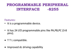
  • 1. PROGRAMMABLE PERIPHERAL INTERFACE -8255 Features: • It is a programmable device. • It has 24 I/O programmable pins like PA,PB,PC (3-8 pins).  T T L compatible.  Improved dc driving capability
  • 3. Function of pins: • Data bus(D0-D7):These are 8-bit bi-directional buses, connected to 8085 data bus for transferring data. • CS: This is Active Low signal. When it is low, then data is transfer from 8085. • Read: This is Active Low signal, when it is Low read operation will be start. • Write: This is Active Low signal, when it is Low Write operation will be start.
  • 4. A1 A0 Select 0 0 PA 0 1 PB 1 0 PC 1 1 Control reg. • Address (A0-A1):This is used to select the ports. like this
  • 5. • RESET: This is used to reset the device. That means clear control registers. • PA0-PA7:It is the 8-bit bi-directional I/O pins used to send the data to peripheral or or to receive the data from peripheral. • PB0-PB7:Similar to PA • PC0-PC7:This is also 8-bit bidirectional I/O pins. These lines are divided into two groups. 1. PC0 to PC3(Lower Groups) 2. PC4 to PC7 (Higher groups) These two groups working in separately using 4 data’s.
  • 7. Data Bus buffer: • It is a 8-bit bidirectional Data bus. • Used to interface between 8255 data bus with system bus. • The internal data bus and Outer pins D0-D7 pins are connected in internally. • The direction of data buffer is decided by Read/Control Logic.
  • 8. Read/Write Control Logic: • This is getting the input signals from control bus and Address bus • Control signal are RD and WR. • Address signals are A0,A1,and CS. • 8255 operation is enabled or disabled by CS.
  • 9. Group A and Group B control: • Group A and B get the Control Signal from CPU and send the command to the individual control blocks. • Group A send the control signal to port A and Port C (Upper) PC7-PC4. • Group B send the control signal to port B and Port C (Lower) PC3-PC0. PORT A: • This is a 8-bit buffered I/O latch. • It can be programmed by mode 0 , mode 1, mode 2 .
  • 10. PORT B: • This is a 8-bit buffer I/O latch. • It can be programmed by mode 0 and mode 1. PORT C: • This is a 8-bit Unlatched buffer Input and an Output latch. • It is splitted into two parts. • It can be programmed by bit set/reset operation.
  • 11. Operation modes: BIT SET/RESET MODE: • The PORT C can be Set or Reset by sending OUT instruction to the CONTROL registers. I/O MODES: • MODE 0(Simple input / Output): • In this mode , port A, port B and port C is used as individually (Simply). • Features: • Outputs are latched , Inputs are buffered not latched. • Ports do not have Handshake or interrupt capability.
  • 12. MODE 1 :(Input/output with Hand shake) • In this mode, input or output is transferred by hand shaking Signals. • Handshaking signals is used to transfer data between whose data transfer is not same. Computer Printer DATA BUS STB ACK Busy
  • 13. Example: • The computer send the data to the printer large speed compared to the printer. • When computer send the data according to the printer speed at the time only, printer can accept. • If printer is not ready to accept the data then after sending the data bus , computer uses another handshaking signal to tell printer that valid data is available on the data bus. • Each port uses three lines from port C as handshake signals
  • 14. MODE 2:Bi-directional I/O data transfer: • This mode allows bidirectional data transfer over a single 8-bit data bus using handshake signals. • This feature is possible only Group A • Port A is working as 8-biy bidirectional. • PC3-PC7 is used for handshaking purpose. • The data is sent by CPU through this port , when the peripheral request it. CONTROL WORD FORMATS: • In the INPUT mode , When RESET is High all 24 pins (3-ports) be a input mode.
  • 15. • i.e all flip flops are cleared and the interrupts are rest. • This condition is maintained even after RESET goes low. • This can be avoid by writing single control word to the control registers , when required.
  • 17. FOR BIT SET/RESET MODE: • This is bit set/reset control word format. X X X Don’t care Bit select B0 B1 B2 D7 D6 D5 D4 D3 D2 D1 D0 0 1 2 3 4 5 6 7 0 1 0 1 0 1 0 1 0 0 1 1 0 0 1 1 0 0 0 0 1 1 1 1 BIT SET/RESET 1=SET 0=RESET BIT SET/RESET FLAG =0 Active
  • 18. • PC0-PC7 is set or reset as per the status of D0. • A BSR word is written for each bit • Example: • PC3 is Set then control register will be 0XXX0111. • PC4 is Reset then control register will be 0XXX01000. • X is a don’t care.
  • 19. • FOR I/O MODE: The mode format for I/O as shown in figure D7 D6 D5 D4 D3 D2 D1 D0 Group A Port C Upper 1=Input 0=Output Port B 1=Input 0=Output Mode selection 00=mode 0 01=mode 1 1x=mode 2 Group B Port C Lower 1=Input 0=Output Port B 1=Input 0=Output Mode selection 0=mode 0 1=mode 1 Mode set flag=1=Active
  • 20. • The control word for both mode is same. • Bit D7 is used for specifying whether word loaded in to Bit set/reset mode or Mode definition word. • D7=1=Mode definition mode. • D7=0=Bit set/Reset mode.
  • 21. 8254 Prgrammable Interval Timer Features of 8254 Prgrammable Interval Timer Three independent 16 bit down counters. Counters can be programmed in 6 different programmable counter modes. Counting facility in both binary or BCD number system. Compatible with Intel and other microprocessor. Single +5 V supply. 24 Pin dual in-line package.
  • 23. Pin description of 8254 PIT
  • 25. This device is useful whenever the microprocessor must control real-time events. The timer in a personal computer is an 8254. To operate a counter a 16-bit count is loaded in its register and on command, it begins to decrement the count until it reaches 0. At the end of the count it generates a pulse, which interrupts the processor. The count can count either in binary or BCD Each counter in the block diagram has 3 logical lines connected to it. Two of these lines, clock and gate, are inputs. The third, labeled OUT is an output. Data bus buffer- It is a communication path between the timer and the microprocessor. The buffer is 8-bit and bidirectional. It is connected to the data bus of the microprocessor. Read /write logic controls the reading and the writing of the counter registers. Control word register, specifies the counter to be used and either a Read or a write operation. Data is transmitted or received by the buffer upon execution of INPUT instruction from CPU. The data bus buffer has three basic functions, Programming the modes of 8254. Loading the count value in timers Reading the count value from timers The data bus buffer is connected to microprocessor using D7 – D0 pins which are also bidirectional. The data transfer is through these pins. These pins will be in high- impedance (or this state) condition until the 8254 is selected by a LOW or CS and either the read operation requested by a LOW RD on the input or a write operation WR requested by the input going LOW.
  • 26. Read/ Write Logic: It accepts inputs for the system control bus and in turn generation the control signals for overall device operation. It is enabled or disabled by CS so that no operation can occur to change the function unless the device has been selected as the system logic. CS : The chip select input is used to enable the communicate between 8254 and the microprocessor by means of data bus. A low an CS enables the data bus buffers, while a high disable the buffer. The CS input does not have any affect on the operation of three times once they have been initialized. The normal configuration of a system employs an decode logic which actives CS line, whenever a specific set of addresses that correspond to 8254 appear on the address bus. RD & WR :The read ( RD ) and write WR pins central the direction of data transfer on the 8-bit bus. When the input RD pin is low. Then CPU is inputting data from 8254 in the form of counter value. When WR pins is low, then CPU is sending data to 8254 in the form of mode information or loading counters. The RD &WR should not both be low simultaneously. When RD & WR pins are HIGH, the data bus buffer is disabled. A0 & A1:These two input lines allow the microprocessor to specify which one of the internal register in the 8254 is going to be used for the data transfer. Fig shows how these two lines are used to select either the control word register or one of the 16-bit counters. A1 A0 Function 0 0 Counter 0 0 1 Counter 1 1 0 Counter 2 1 1 Control Word
  • 27. Control word register: It is selected when A0 and A1 . It the accepts information from the data bus buffer and stores it in a register. The information stored in then register controls the operation mode of each counter, selection of binary or BCD counting and the loading of each counting and the loading of each count register. This register can be written into, no read operation of this content is available. Counters: Each of the times has three pins associated with it. These are CLK (CLK) the gate (GATE) and the output (OUT). CLK: This clock input pin provides 16-bit times with the signal to causes the times to decrement maximum clock input is 2.6MHz. Note that the counters operate at the negative edge (H1 to L0) of this clock input. If the signal on this pin is generated by a fixed oscillator then the user has implemented a standard timer. If the input signal is a string of randomly occurring pulses, then it is called implementation of a counter. GATE: The gate input pin is used to initiate or enable counting. The exact effect of the gate signal Depends on which of the six modes of operation is chosen. OUTPUT: The output pin provides an output from the timer. It actual use depends on the mode of Operation of the timer. The counter can be read ―in the fly‖ without inhibiting gate pulse or clock input.
  • 28. Control word register Format of 8254
  • 29. Modes Of Operation •Mode 0: Interrupt On Terminal Count, •Mode 1: Programmable One Shot, •Mode 2: Rate Generator , •Mode 3: Square Wave Rate Generator •Mode 4: Software Triggered Strobe •Mode 5: Hardware Triggered Strobe
  • 30. Programmable Interrupt Controller-8259 Features of The 8259  8259 is a programmable interrupt controller specially designed to work with Intel microprocessor 8080, 8085A, 8086, 8088.  It can handle eight interrupt inputs. This is equivalent to providing eight interrupt pins on the processor in place of one INTR (in 8085A)/INT(in 8086) pin.  It can resolve eight levels of interrupt priorities in a variety of modes. The priorities of interrupts can be changed under running condition. Some of the desired lower priority interrupts may be allowed to be acknowledged during the service of higher priority interrupts.
  • 31.  Each of the interrupt requests can be masked individually similar to RST7.5, RST6.5 and RST5.5 interrupts of 8085A.  The status of pending interrupts, in service interrupts,and masked interrupts can be read at any time similar to RST interrupts of 8085A.  The chip can be programmed to accept interrupt requests either as level triggered or edge triggered interrupt request unlike your RST interrupts where some are edge triggered and some are level triggered. However, all interrupts must be either level triggered or edge triggered.  If required, nine 8259As can be cascaded in a master-slave configuration mode to handle 64 interrupt inputs. In this case, the interrupting devices send their interrupt requests either to slave 8259A or to master 8259A directly. The slave 8259As send their interrupt to master interrupt request inputs and the master will send a single interrupt to microprocessor interrupt pin
  • 32. Pin Configuration of Intel 8259A
  • 33. • The 8259 A is contained in a 28 dual-in-line package that requires only +5V supply voltage. The 8259A is upward compatible with 8259. The main difference between the two is that the 8259A can be used with Intel 8086/8088 processor. It also includes additional features such as level triggered mode, buffered mode and automatic end of interrupt mode. • The pin diagram and internal block diagram of PIC is shown in figure. The pins are defined as follows:  CS (Chip Select signal): To access this chip, chip select signal CS is made low. A LOW on this pin enables RD & WR communication between the CPU and the 8259A. This signal is made LOW by decoding the addresses assigned to this chip. Therefore, this pin is connected to address bus through the decoder logic circuit. Interrupt acknowledge functions to transfer the control to interrupt service subroutine are independent of CS .
  • 34.  WR (Write signal): A low on this pin. When CS is low enables the 8259 A to accept command words from CPU.  RD (Read signal): A low on this pin when CS is low enables this 8259A to release status (pending interrupts or in-service interrupts or masked interrupts) on to the data bus for the CPU. The status includes the contents of IMR (interrupt mask register) or ISR(interrupt service register) or IRR (interrupt request register) or a priority level.  D7-D0 (Data Bus): Bidirectional data bus. Control, status and interrupt vector information is transferred via this data bus. This bus is connected to BDB of 8085A. CAS2-CAS0 (Cascade lines): The CAS2-0 lines form a local 8259A bus to control multiple 8259As in master-slave configuration, i.e., to identify a particular slave 8259A to be accessed for transfer of vector information. These pins are automatically set as output pins for master 8259A and input pins for a slave 8259A once the chips are programmed as master or slave.
  • 35.  SP / EN (Salve Program/Enable Buffer): This is a dual function pin. When the chip is programmed in buffered mode, the pin can be used as an output and when not in the buffered mode it is used as an input. In non-buffered mode it is used as an input pin to determine whether the 8259A is to be used as a master (SP / EN = 1) or as a slave (SP / EN = 0). In buffered mode, normally data bus buffers are used. These buffers need to be enabled or disabled during transfer of vector information depending upon whether 80259A is connected before the buffer or after the buffer. To disable/enable the data bus transceivers (buffers) when data are being transferred from the 8259A to the CPU, this pin is made low or high.  INT (Interrupt output): This pin goes high whenever a valid interrupt request is asserted. It is used to interrupt the CPU, thus it is connected to the CPU’s interrupt pin (INTR). In case of master-slave configuration, the interrupt pin of slave 8259A is connected to interrupt request input of master 8259A.
  • 36. INTA (Interrupt Acknowledge): This pin is used to enable 8259A interrupt vector data on the data bus by a sequence of interrupt acknowledge pulses issued by the CPU. IR0-IR7 (Interrupt Request inputs): These are asynchronous interrupt request input pins. An interrupt request is executed by raising an IR input (low to high), and holding it high until it is acknowledged. (Edge triggered mode) or just by a high level on an interrupt request input (Level triggered mode). A0 (A0 address line): This pin acts in conjunction with the RD , WR &CS pins. It is used by the 8259A to send various command words from the CPU and to read the status. It is normally connected to the CPU A0 address line. Two addresses are assigned/ reserved in the I/O address space for each 8259A in the system- one with A0 =0 is called even address and other with A0 = 1 is called odd address.
  • 38. Functional Description of 8259:  The 8259A (PIC) has eight interrupt request inputs – IR7 -IR0.The 8259A uses its INT output to interrupt the 8086 via INTR pin. The 8259A receives interrupt acknowledge pulses from the 𝜇𝑝 at its INTA input. Vector address, used by the 8086 to transfer control to the service subroutine of the interrupting device, is provided by the 8259A on the data bus. The 8259A is a programmable device that must be initialized by command words sent by the microprocessor. After initialization the 8259A mode of operation can be changed by operation command words from the microprocessor
  • 39. Data bus buffer: This 3- state, bidirectional 8-bit buffer is used to interface the 8259A to the system data bus. Control words and status information from the microprocessor to PIC and from PIC to microprocessor respectively, are transferred through the data bus buffer. Read/Write & Control Logic: The function of this block is to accept output commands sent from the CPU. It contains the initialization command word (ICW) registers and operation command word (OCW) registers which store the various control formats for device operation. This function block also allows the status of 8259A to be transferred to the data bus. Interrupt Request Register (IRR): Interrupt request register (IRR) stores all the interrupt inputs that are requesting service. It is an 8-bit register – one bit for each interrupt request. Basically, it keeps track of which interrupt inputs are asking for service. If an interrupt input is unmasked, and has an interrupt signal on it, then the corresponding bit in the IRR will be set. The content of this register can be read to know the status of pending interrupts.
  • 40. Interrupt Mask Register (IMR): The IMR is used to disable (Mask)or enable (Unmask) individual interrupt request inputs. This is also an 8-bit register. Each bit in this register corresponds to the interrupt input with the same number. The IMR operates on the IRR. Masking of higher priority input will not affect the interrupt request lines of lower priority. To unmask any interrupt the corresponding bit is set ‘0’. In-service Register (ISR): The in-service register keeps track of which interrupt inputs are currently being serviced. For each input that is currently being serviced the corresponding bit of in-service register (ISR) will be set. In 8259A, during the service of an interrupt request, if another higher priority interrupt becomes active, it will be acknowledged and the control will be transferred from lower priority interrupt service subroutine (ISS) to higher priority ISS. Thus, more than one bit of ISR will be set indicating the number of interrupts being serviced. Each of these 3-registers can be read as status register.
  • 41. Priority Resolver: This logic block determines the priorities of the interrupts set in the IRR. It takes the information from IRR, IMR and ISR to determine whether the new interrupt request is having highest priority or not. If the new interrupt request is having the highest priority, it is selected and processed. The corresponding bit of ISR will be set during interrupt acknowledge machine cycle. Cascade Buffer/Comparator: This function block stores and compares the IDs of all 8259A’s in the system. The associated 3-I/O lines (CAS2-CAS0) are outputs when 8259A is used as a master and are inputs when 8259A is used as a slave. As a master, the 8259A sends the ID of the interrupting slave device onto the CAS2- CAS0 lines. The slave 8259As compare this ID with their own programmed ID. Thus selected 8259A will send its pre-programmed subroutine address on to the data bus during the next one or two successive INTA pulses.
  • 42. • For master 8259 these pins are outputs and for slaves these are inputs. • When 8259 is a master the CALL op-code is generated by master in response to the first Interrupt acknowledge. • The vectoring address must be released by slave 8259 • The master puts out the identification code to select one of the slave from 8 slaves through these pins. • The slave accepts these three signals as inputs and compare the code put out by the master with the codes assigned to them during initialization. • The slave thus selected puts out the address of ISR during second and third interrupt acknowledge pulses from the CPU.
  • 43. Slave Program/ Enable Buffer: SP/EN • Used to specify whether 8259 is to act as a master or a slave  High-Master  Low – Slave • In Non-Buffered Mode, this pin is used to specify whether 8259 is to act as a master or a slave. • In Buffered mode this pin is used as an output to enable the data bus buffer of the system.
  • 44. 8259APIC- Interrupt Operation • To implement interrupt, the interrupt Enable FF must be enabled by writing EI instruction. • 8259A- should be initialized by writing control words in the control register. • 8259 requires two types of control words: ICW- Used to set up proper conditions  And specify RST vector address. OCW- Used to perform functions such as  Masking interrupts, setting up status  Read operations etc. After 8259A is initialized, the following sequence of events occurs when one or more interrupt request lines go high.
  • 45. 1. IRR stores the Interrupt requests. 2. Priority Resolver Checks three registers: IRR-for interrupt requests. IMR- for Masking bits. ISR- for the interrupt request being serviced. It resolves the priority and sets the INT high when appropriate. 3. MPU acknowledges the interrupt by sending interrupt acknowledge. 4. After INTA is received, the appropriate priority bit in the ISR is set to indicate which level is being served and the corresponding bit in the IRR is reset to that request is accepted. Then op-code for CALL instruction is placed on the Data Bus. 5. When MPU decodes the CALL instruction, it places two more signals on the data bus. 6. When 8259 receives second INTA , it places lower order byte of CALL address on the data bus. Third INTA High order byte. The CALL address is the vector memory location for the interrupt. This address is placed in control register during Initialization.
  • 46. • During third INTA pulse, the ISR bit is reset either automatically (AEOI) or by a command word that must be issued at the end of the service routine (EOI). This option is determined by the ICW. 8. The program sequence is transferred to thememory location specified by the CALL Instruction.  AEOI - Automatic End of Interrupt Mode  EOI - End of Interrupt Mode
  • 47. 8259 System bus interface
  • 48. 8259A PIC- COMMAND WORDS • Two types: ICW, OCW ICW: • Before start functioning, 8259 must be initialized by writing two to four command words into their respective command word registers. • A0=0,D4=1: The control word is ICW1.ICW1-contains the control bits for edge/level triggered mode, single/cascade mode, call address interval and whether ICW4 is required or not etc. • A0=1: ICW2- Store details interrupt vector addresses.
  • 49. 8259A PIC- ICW1  The following initialization procedure Carried out internally when ICW1is loaded. 1. The edge sense circuit is reset i.e. by default 8259A interrupts are edge sensitive. 2. IMR is cleared. 3. IR7 input is assigned lowest priority. 4. Slave mode address is set to 7. 5. Special mask mode is cleared and status read is set to IRR. 6. If IC4=0, all functions of ICW4 are set to Zero. Master/slave bit in ICW4 bit is used in buffered mode only
  • 51. ICW1:
  • 52. ICW2:
  • 53. ICW3:
  • 54. ICW4:
  • 55. Operation Command Word 1 (OCW 1): • A Write command to the 8259 with A0 = 1 (after ICW2) is interpreted as OCW1. OCW1 is used for enabling or disabling the recognition of specific interrupt requests by programming the IMR. • M = 1 indicates that the interrupt is to be masked, and M = 0 indicates that it is to be unmasked
  • 56. Operation Command Word 2 (OCW2): • A Write command with A0 = 1 and D4 D3 = 00 is interpreted as OCW2. The R (Rotate), SL (Select-Level), EOI bits control the Rotate and End Of Interrupt Modes and combinations of the two. • Figure shows the Operation Command Word format. L2-L0 are used to specify the interrupt level to be acted upon when the SL bit is active.
  • 57. Operation Command Word 2 (OCW2): • When the ESMM (Enable special mask mode ) bit is set, then the SMM bit is don’t care. If SMM = 1 and ESMM = 1, then 8259 will enter in Special mask mode. • If ESMM = 1 and SMM = 0, then 8259 will return into normal mask mode. • RR and RIS are used to give the read register command. • P = 1 is used for poll command.