Downloaded 105 times
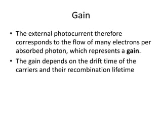
![Shot noise current: Dark current
• The root mean square (rms) value of the
fluctuations in the dark current represents
the shot noise current:
in-dark=[2eId B] ½ (1)
where B is the frequency bandwidth of the
photodetector.
• The photocurrent signal must be greater than
this shot noise in the dark current](https://image.slidesharecdn.com/chapter6b-140705120956-phpapp02/85/Chapter-6b-15-320.jpg)
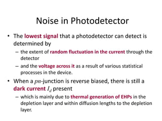
![Shot Noise Current: Quantum Noise
• The photocurrent will always
– exhibit fluctuations about its mean value due to
quantum noise.
• If Iph is the mean photocurrent, the
fluctuations about this mean has an rms value
that is called shot noise current due to
quantum noise,
in-quantum=[2 e Iph B] ½ (2)](https://image.slidesharecdn.com/chapter6b-140705120956-phpapp02/85/Chapter-6b-17-320.jpg)
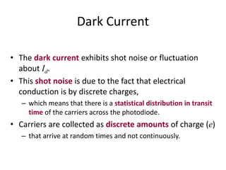
![RMS total shot noise current
• Generally, the dark current shot noise and quantum
noise are the main sources of noise in pn-junction
and pin type photodiodes.
• The total shot noise generated by the photodetector
is not a simple sum of eqns (1) & (2) because the two
processes are due to independent random
fluctuations
• We need to add the mean squares of the shot noise
current
i2
n= i2
n-dark + i2
n-quantum
i2
n= [2 e (Id + Iph ) B]](https://image.slidesharecdn.com/chapter6b-140705120956-phpapp02/85/Chapter-6b-19-320.jpg)
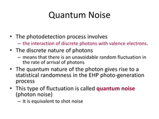
![Quantitative definition of NEP
• If R is the responsivity and Po is the monochromatic
incident optical power then the generated
photocurrent is, Iph = RPo
• Suppose Iph = in when Po = P1,
Then RP1 = [2 e (Id + Iph ) B] ½
• From this, we find optical power per square root of
frequency bandwidth as
P1/ B½ = (1/R)[2 e (Id + Iph ) ] ½
• Quantitative definition of NEP = P1/ B½ [W Hz –½]
• If we put B = 1 Hz, NEP = P1](https://image.slidesharecdn.com/chapter6b-140705120956-phpapp02/85/Chapter-6b-23-320.jpg)

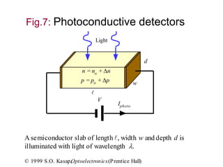
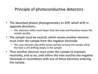
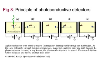
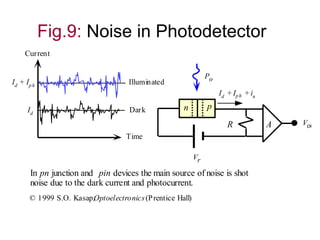
The document summarizes the operating principles of phototransistors and photoconductive detectors. - Phototransistors are bipolar junction transistors that use the photocurrent generated in the base-collector junction to inject a multiplied current into the emitter circuit, similar to a common emitter transistor. The photocurrent acts as the base current. - Photoconductive detectors have two electrodes attached to a light-absorbing semiconductor. Absorbed photons increase conductivity and the external photocurrent. With ohmic contacts, multiple electrons enter the semiconductor for each hole, producing photoconductive gain. - The main sources of noise in photodetectors are shot noise from the dark current and photocurrent. The total noise


![Chp1 1 bjt [read only]](https://cdn.slidesharecdn.com/ss_thumbnails/chp11bjtread-only-130929091550-phpapp02-thumbnail.jpg?width=640&height=640&fit=bounds)


![ANIMAL_CELL_,_TISSUE_AND_ORGAN_CULTURE[1].pptx](https://cdn.slidesharecdn.com/ss_thumbnails/animalcelltissueandorganculture1-260204172026-4462b440-thumbnail.jpg?width=640&height=640&fit=bounds)


