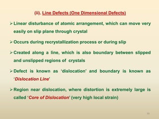
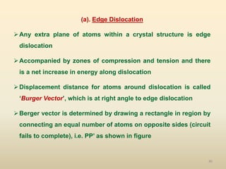
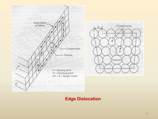
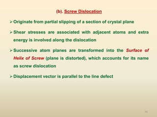
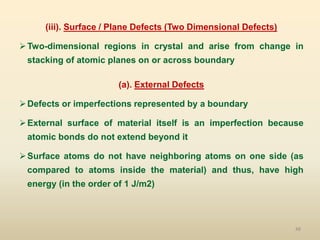
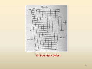
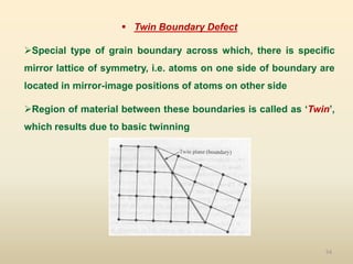
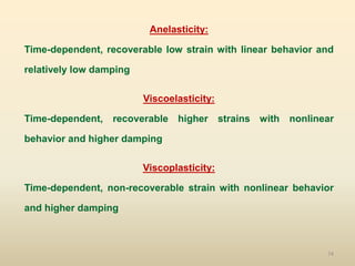
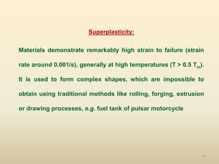
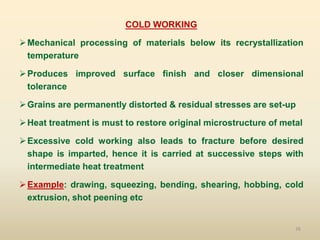
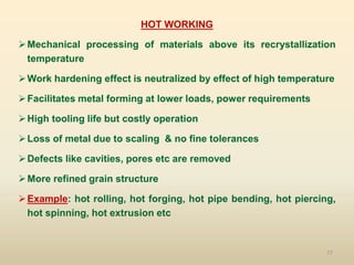
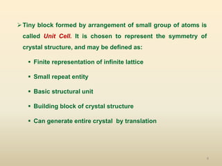
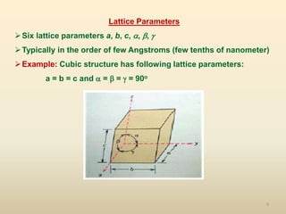
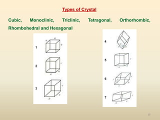
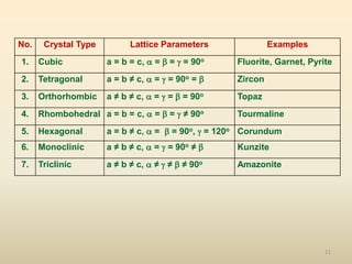
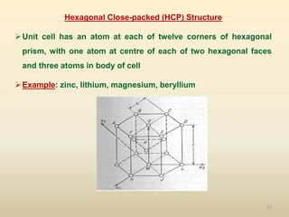
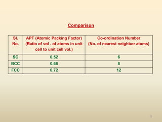
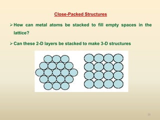
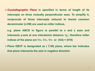
The document provides an overview of crystal structures and imperfections in solids, detailing types of crystal lattices, their geometric properties, and atomic arrangements. It discusses common defects in crystals, including point, line, surface, and volume defects, along with their formation and implications on material properties. Additionally, it covers the concepts of elastic and plastic deformation, highlighting the behavior of materials under stress and the differences between elastic recovery and permanent deformation.


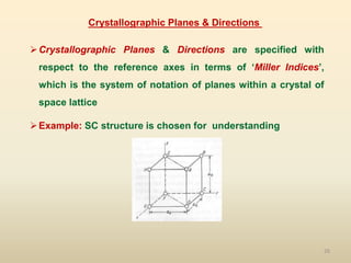
![28
Crystallographic Directions are indicated by integers in
brackets like [uvw], where reciprocals are never used, e.g.
direction ‘FD’ is obtained by moving out from origin, a
distance ‘a0’ along positive x-axis and moving same distance
along positive y-axis also, therefore, the crystallographic
direction will be given as [110]
Example: Ionic crystals like NaCl, LiF (not for metals)
Note: For simple cubic lattice only, direction is always
perpendicular the plane having same indices](https://image.slidesharecdn.com/module2inmperfectionsincrystals-191204183837/85/inmperfections-in-crystals-28-320.jpg)