Download to read offline
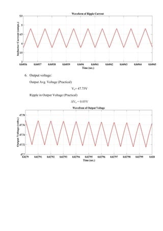

The document describes simulating a boost converter circuit using MATLAB/Simulink. Key parameters of the boost converter include an input voltage of 24V, output voltage of 48V at 100W, and switching frequency of 100kHz. The design procedure involves calculating the duty ratio, average inductor current, inductor and capacitor values to achieve the desired output voltage while limiting current and voltage ripple. Simulation results show the input voltage, switching signal, component voltages and currents match the theoretical values closely.