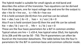
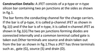
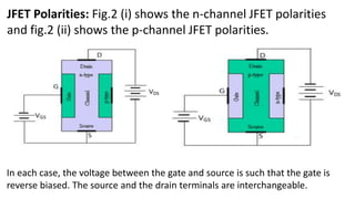
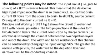
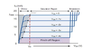
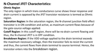
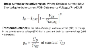
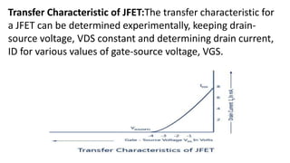
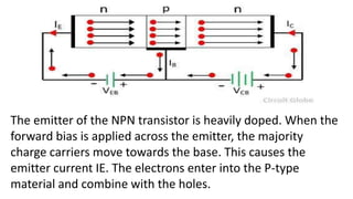
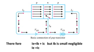
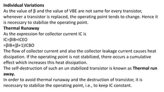
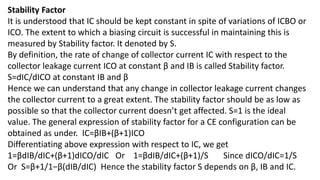
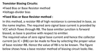
The document discusses bipolar junction transistors and junction field effect transistors. It describes:
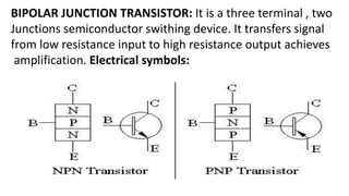
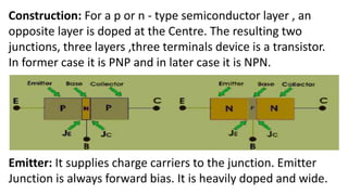
1) The construction and working of NPN and PNP bipolar junction transistors, including the roles of the emitter, base, and collector. Current flows from the emitter to the collector when the base is forward biased.
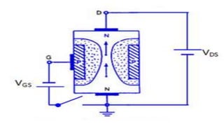
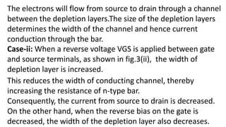
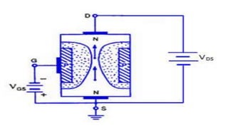
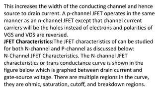
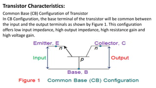
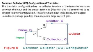
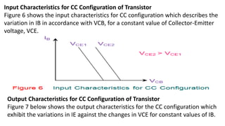
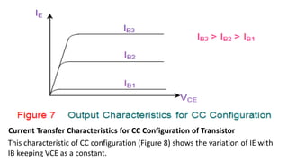
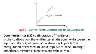
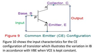
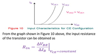
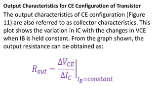
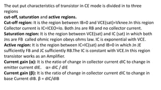
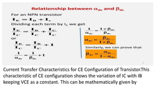
2) The common base, common collector, and common emitter configurations of transistors and their input, output, and current transfer characteristics.
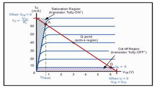
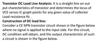
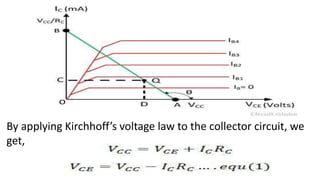
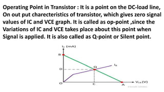
3) Transistor DC load line analysis which determines the operating point where variations in collector current and voltage occur when a signal is applied.


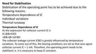
![Collector Current, IC
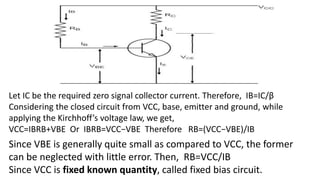
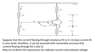
From the circuit, it is evident that,
I1=VCC/(R1+R2)
Therefore, the voltage across resistance R2 is
V2=[VCC/(R1+R2)]R2
Applying Kirchhoff’s voltage law to the base circuit,
V2=VBE+VE
V2=VBE+IERE
IE=(V2−VBE)/RE
Since IE ≈ IC,
IC=(V2−VBE)/RE
From the above expression, it is evident that IC doesn’t depend upon β. VBE is
very small that IC doesn’t get affected by VBE at all. Thus IC in this circuit is
almost independent of transistor parameters and hence good stabilization is
achieved.](https://image.slidesharecdn.com/cbcse1unit-3-210128064111/85/Cbcs-e1-unit-3-44-320.jpg)