Downloaded 131 times

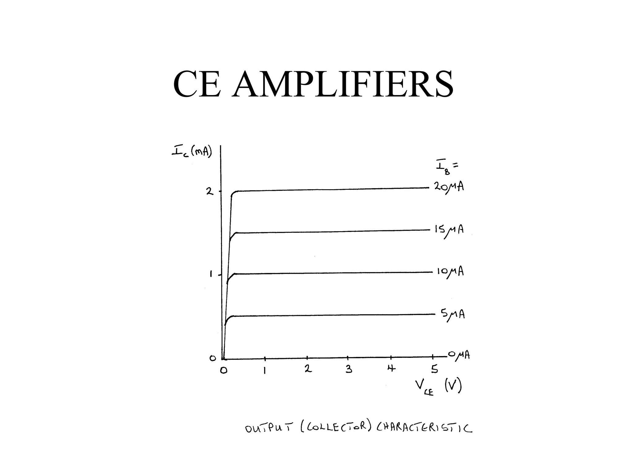
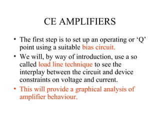
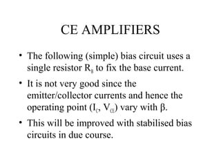
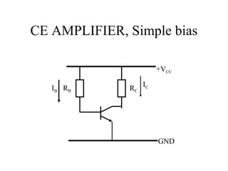
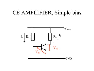


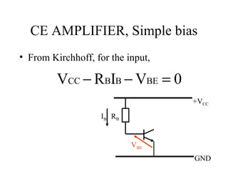

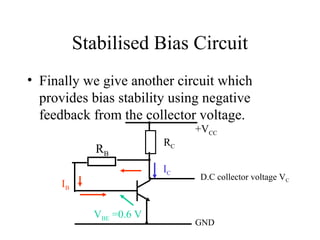
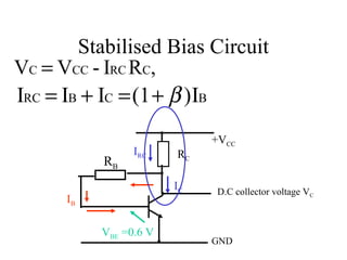
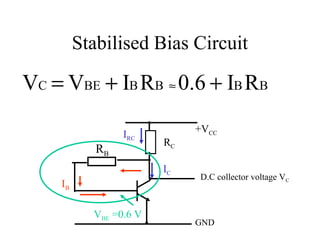
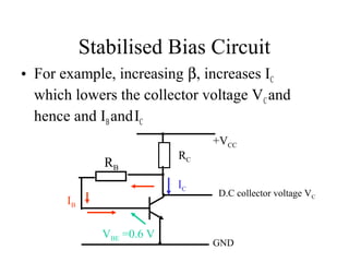

1) CE amplifiers use bias circuits to set an operating point for the transistor. Simple bias circuits vary with transistor parameters like beta. 2) Load line analysis graphs the interplay between circuit constraints and the transistor output characteristic to determine the operating point. 3) Stabilized bias circuits aim to fix the emitter current independently of beta using an emitter resistor and potential divider bias network. Negative feedback bias circuits also use feedback from the collector voltage.


