ER Publication,
IJETR, IJMCTR,
Journals,
International Journals,
High Impact Journals,
Monthly Journal,
Good quality Journals,
Research,
Research Papers,
Research Article,
Free Journals, Open access Journals,
erpublication.org,
Engineering Journal,
Science Journals,
High Frequency Soft Switching Of PWM Boost Converter Using Auxiliary Resonant...IJERA Editor
This thesis presents High frequency Soft Switching DC-DC boost Converter. The circuit consists of a general Boost Converter with an additional resonant circuit which has a switch, inductor, capacitor and a diode.In general Boost Converter circuits have snubber circuits where switching losses are dissipated in external passive resistors; which is known as hard switching. As the switching frequency of PWM converters is increased its switching losses and conduction losses also increases. This restricts the use of PWM technique. New Zero Voltage Transition-Zero Current Transition (ZVT-ZCT) PWM converter equipped with the snubber provides the most desirable features of both ZVT and ZCT converters presented previously. Moreover all semiconductors devices operate with soft switching and hence losses are reduced.
SIMULATION ANALYSIS OF CLOSED LOOP DUAL INDUCTOR CURRENT-FED PUSH-PULL CONVER...Journal For Research
The current electronic devices require DC power source, which is taken from a battery or DC power supply. DC-DC converter is utilized to get regulated dc voltage from unregulated one. Switched mode power supply (SMPS) are commonly used in industrial applications, because of more advantages compared to linear power supply. In SMPS we have isolated and non-isolated converters, where isolated converters are frequently used, in order to get more voltage with multiple outputs. So among different isolated converters, push-pull converter is chosen for micro converter applications to obtain high voltage conversion ratio by using HF transformer, due to their better utilization of transformer. New methodology of control is implemented for making ZVS and ZCS at same time and to reduce the number of switches in the secondary side of dual inductor CFPP converter, which is a voltage doubler circuit. This becomes the solution for problem identification. Thus this converter with soft-switching reduces the switching losses.The current-fed push-pull converters are used in many applications like photo-voltaic (PV) power converters for boosting the output voltage. Push-pull converter is chosen for micro converter applications, to obtain high voltage conversion ratio by using high frequency (HF) transformer, due to their better utilization of transformer. This deals with the design of dual inductor CFPP converter, where zero voltage switching (ZVS) and zero current switching (ZCS) is achieved for the primary side of the converter by using secondary switches. Primary side switches are controlled by closed loop control topology. The secondary side is made with voltage doubler to obtain high voltage. Open loop and closed loop control of dual inductor current fed push pull converter simulation is finished by MATLAB/SIMULINK and their outcomes are analyzed.
Starting of fluorescent tube light by using inverter circuit instead of choke...IJERA Editor
A fluorescent tube light generally starts glowing when a large voltage is applied across its terminals at the time
of starting for a very short period, once it starts glowing then it will be able to continue with normal supply
voltage. Conventionally this needed high voltage, at the time of starting, is provided by the use of choke starter
arrangement.On the other hand, the circuit which converts the dc into ac is called inverter circuit. This paper
will discuss about an inverter circuit which can be used in place of choke starter arrangement. This inverter
circuit develops high voltage at the time of starting and after that its output voltage will come down to the
normal rated voltage level. This inverter circuit arrangement not only make the tube light performance faster but
also economically preferable.
Report On diode clamp three level inverterVinay Singh
three level diode clamp inverter. that converts any type of DC ( rectified, PV cell, battery etc.) to AC supply. we made by mosfet and ardiuno . in this ppt we present the Simulink model of a three-level inverter and the hardware reort of the inverter.
also discuss about other level inverter and there THD analysis, simulink model and detail. compression between another inverter.
The International Journal of Engineering & Science is aimed at providing a platform for researchers, engineers, scientists, or educators to publish their original research results, to exchange new ideas, to disseminate information in innovative designs, engineering experiences and technological skills. It is also the Journal's objective to promote engineering and technology education. All papers submitted to the Journal will be blind peer-reviewed. Only original articles will be published.
A DC-DC converter topology is presented
combining the soft switching effects of the Snubber Assisted Zero
Voltage and Zero Current Transition (SAZZ) topology and the
increased inductor frequency of the dual interleaved boost
converter with interphase transformer. The snubber capacitors
and output capacitances of the main devices are discharged prior
to turn on using a single auxiliary inductor, eliminating turn on
losses. Furthermore, the turn off losses are significantly reduced
since the energy stored in the device output capacitance at turn
off is recovered at turn on. The effectiveness of the topology is
demonstrated on a SiC prototype operating at 12.5 kW, 112 kHz,
reducing the switching losses by 50%.
Microcontroller Based Novel Dc-to-Ac Grid Connected Inverter TopologyIDES Editor
The conventional line commutated ac-to-dc
converters/ inverters have square-shaped line current which
contains higher-order harmonics. Moreover, it requires a
costly and bulky dc inductor or choke. The line current with
the high harmonic contents generates EMI and therefore it
causes more heating of the core of distribution or power
transformers. Alternatively, PWM based inverters using
MOSFET/IGBT switches can be used for the above purpose.
However, apart from higher switching losses, the power
handling capability and reliability of these devices are quite
low in comparison to thyristors/ SCR. A thyristor based forced
commutated inverters are not suitable for PWM applications
due to the problems of commutation circuits. A pure sinusoidal
voltage output or waveform with low harmonic contents is
most desirable in the conversion from dc to ac. In the present
work, a novel two pulse line commutated inverter is been
proposed with control signal generated from PIC 16F 877A. It
improves the wave shape hence it reduces the total harmonic
distortion (THD) of the grid interactive-inverter. The
simulation of the circuit is done using SIMULINK. Moreover,
the performance of the proposed circuitry is far better than
the conventional line-commutated inverter. It reduces THD,
number of thyristors and dispenses with the bulky dc inductor/
choke. A prototype model is developed for discontinuous line
current mode. The results are also compared with the
simulation results in SIMULINK/ MATLAB.
Simulation of Five Level Diode Clamped Multilevel Inverterrahulmonikasharma
The power electronics device which converts DC power to AC power at required output voltage and frequency level is known as inverter. The voltage source inverters produce an output voltage or a current with levels either 0 or +ve or-ve V dc. They are known as two-level inverters. Multilevel inverter is to synthesize a near sinusoidal voltage from several levels of dc voltages. Multilevel inverter has advantage like minimum harmonic distortion. Multi-level inverters are emerging as the new breed of power converter options for high power applications. They typically synthesize the stair-case voltage waveform (from several dc sources) which has reduced harmonic content. Multi-level inverters have many attractive features, high voltage capability, reduced common mode voltages near sinusoidal outputs, low dv/dt, and smaller or even no output filter; sometimes no transformer is required at the input side, called the transformer-less solution, making them suitable for high power applications In this paper a 5-level Diode clamped multilevel inverter is developed by IGBTS using Simulink. Gating signals for these IGBTS have been generated by designing comparators. In order to maintain the different voltage levels at appropriate intervals, the conduction time intervals of IGBT have been maintained by controlling the pulse width of gating pulses[6] (by varying the reference signals magnitude of the comparator). The simulation results for 5-level and THD for the output have been identified by MATLAB/SIMULINK.
Three Phase Controlled Rectifier Study in Terms of firing angle variationsIDES Editor
This paper introduce topology of three phase
controlled rectifiers and proposed an accurate Statistical
method to calculate their input current harmonic components,
and calculate THD and harmonic currents with accurate
simulation in various firing angles, then investigate influence
of load variations in terms of firing angle variations on
harmonic currents. Finally a harmonic current database of
rectiûers is obtained in terms of firing angle and load
variations.
ER Publication,
IJETR, IJMCTR,
Journals,
International Journals,
High Impact Journals,
Monthly Journal,
Good quality Journals,
Research,
Research Papers,
Research Article,
Free Journals, Open access Journals,
erpublication.org,
Engineering Journal,
Science Journals,
ER Publication,
IJETR, IJMCTR,
Journals,
International Journals,
High Impact Journals,
Monthly Journal,
Good quality Journals,
Research,
Research Papers,
Research Article,
Free Journals, Open access Journals,
erpublication.org,
Engineering Journal,
Science Journals,
ER Publication,
IJETR, IJMCTR,
Journals,
International Journals,
High Impact Journals,
Monthly Journal,
Good quality Journals,
Research,
Research Papers,
Research Article,
Free Journals, Open access Journals,
erpublication.org,
Engineering Journal,
Science Journals,
ER Publication,
IJETR, IJMCTR,
Journals,
International Journals,
High Impact Journals,
Monthly Journal,
Good quality Journals,
Research,
Research Papers,
Research Article,
Free Journals, Open access Journals,
erpublication.org,
Engineering Journal,
Science Journals,
ER Publication,
IJETR, IJMCTR,
Journals,
International Journals,
High Impact Journals,
Monthly Journal,
Good quality Journals,
Research,
Research Papers,
Research Article,
Free Journals, Open access Journals,
erpublication.org,
Engineering Journal,
Science Journals,
ER Publication,
IJETR, IJMCTR,
Journals,
International Journals,
High Impact Journals,
Monthly Journal,
Good quality Journals,
Research,
Research Papers,
Research Article,
Free Journals, Open access Journals,
erpublication.org,
Engineering Journal,
Science Journals,
ER Publication,
IJETR, IJMCTR,
Journals,
International Journals,
High Impact Journals,
Monthly Journal,
Good quality Journals,
Research,
Research Papers,
Research Article,
Free Journals, Open access Journals,
erpublication.org,
Engineering Journal,
Science Journals,
ER Publication,
IJETR, IJMCTR,
Journals,
International Journals,
High Impact Journals,
Monthly Journal,
Good quality Journals,
Research,
Research Papers,
Research Article,
Free Journals, Open access Journals,
erpublication.org,
Engineering Journal,
Science Journals,
ER Publication,
IJETR, IJMCTR,
Journals,
International Journals,
High Impact Journals,
Monthly Journal,
Good quality Journals,
Research,
Research Papers,
Research Article,
Free Journals, Open access Journals,
erpublication.org,
Engineering Journal,
Science Journals,
ER Publication,
IJETR, IJMCTR,
Journals,
International Journals,
High Impact Journals,
Monthly Journal,
Good quality Journals,
Research,
Research Papers,
Research Article,
Free Journals, Open access Journals,
erpublication.org,
Engineering Journal,
Science Journals,
ER Publication,
IJETR, IJMCTR,
Journals,
International Journals,
High Impact Journals,
Monthly Journal,
Good quality Journals,
Research,
Research Papers,
Research Article,
Free Journals, Open access Journals,
erpublication.org,
Engineering Journal,
Science Journals,
ER Publication,
IJETR, IJMCTR,
Journals,
International Journals,
High Impact Journals,
Monthly Journal,
Good quality Journals,
Research,
Research Papers,
Research Article,
Free Journals, Open access Journals,
erpublication.org,
Engineering Journal,
Science Journals,
ER Publication,
IJETR, IJMCTR,
Journals,
International Journals,
High Impact Journals,
Monthly Journal,
Good quality Journals,
Research,
Research Papers,
Research Article,
Free Journals, Open access Journals,
erpublication.org,
Engineering Journal,
Science Journals,
ER Publication,
IJETR, IJMCTR,
Journals,
International Journals,
High Impact Journals,
Monthly Journal,
Good quality Journals,
Research,
Research Papers,
Research Article,
Free Journals, Open access Journals,
erpublication.org,
Engineering Journal,
Science Journals,
ER Publication,
IJETR, IJMCTR,
Journals,
International Journals,
High Impact Journals,
Monthly Journal,
Good quality Journals,
Research,
Research Papers,
Research Article,
Free Journals, Open access Journals,
erpublication.org,
Engineering Journal,
Science Journals,
ER Publication,
IJETR, IJMCTR,
Journals,
International Journals,
High Impact Journals,
Monthly Journal,
Good quality Journals,
Research,
Research Papers,
Research Article,
Free Journals, Open access Journals,
erpublication.org,
Engineering Journal,
Science Journals,
9+-
ER Publication,
IJETR, IJMCTR,
Journals,
International Journals,
High Impact Journals,
Monthly Journal,
Good quality Journals,
Research,
Research Papers,
Research Article,
Free Journals, Open access Journals,
erpublication.org,
Engineering Journal,
Science Journals,
ER Publication,
IJETR, IJMCTR,
Journals,
International Journals,
High Impact Journals,
Monthly Journal,
Good quality Journals,
Research,
Research Papers,
Research Article,
Free Journals, Open access Journals,
erpublication.org,
Engineering Journal,
Science Journals,
ER Publication,
IJETR, IJMCTR,
Journals,
International Journals,
High Impact Journals,
Monthly Journal,
Good quality Journals,
Research,
Research Papers,
Research Article,
Free Journals, Open access Journals,
erpublication.org,
Engineering Journal,
Science Journals,
ER Publication,
IJETR, IJMCTR,
Journals,
International Journals,
High Impact Journals,
Monthly Journal,
Good quality Journals,
Research,
Research Papers,
Research Article,
Free Journals, Open access Journals,
erpublication.org,
Engineering Journal,
Science Journals,
Research Inventy : International Journal of Engineering and Science is published by the group of young academic and industrial researchers with 12 Issues per year. It is an online as well as print version open access journal that provides rapid publication (monthly) of articles in all areas of the subject such as: civil, mechanical, chemical, electronic and computer engineering as well as production and information technology. The Journal welcomes the submission of manuscripts that meet the general criteria of significance and scientific excellence. Papers will be published by rapid process within 20 days after acceptance and peer review process takes only 7 days. All articles published in Research Inventy will be peer-reviewed.
Review of Step down Converter with Efficient ZVS OperationIJRST Journal
This paper presents the review of step down converter with efficient ZVS operation. The designed buck converter uses ZCS technique and the function is realized so that the power form is converted from 12V DC 5V DC (1A). A detailed analysis of zero current switching buck converters is performed and a mathematical analysis of the mode of operation is also presented. In order to reduce the switching losses in associated with conventional converters; resonant inductor and resonant capacitor (LC resonant circuit) is applied which helps to turn on-off the switch at zero current. The dc-dc buck converter receives the energy from the input source, when the switch is turned-on. The buck–buck converters have characteristics that warrant a more detailed study. The buck converters under discontinuous conduction mode /continuous conduction mode boundary.
Comparative Steady State Analysis of Boost and Cascaded Boost Converter with ...IAES-IJPEDS
In this paper, an overall comparison between the Boost Converter (BC) &
Cascaded Converter/ Cascaded Boost Converter (CBC) has been depicted in
terms of ideal condition, as well as with the consideration of Equivalent
Series Resistance (ESR) of inductor(s). The loss comparison in the two
converters due to the ESR is also included in this paper. It can be seen that in
CBC, voltage gain is more but the power loss due to ESR is also more
compared to BC. The parameters of the converters are derived with a
consideration of per unit ripple quantity of inductor current and capacitor
voltage. A boundary condition between the continuous conduction mode
(CCM) & discontinuous conduction mode (DCM) of the inductor current is
also shown. The behaviour of the capacitor current for the converters is
discussed during ON and OFF condition of the switch(es) during DCM. At
the end, the simulation results of both the converters are given for a
20V/100V, 100 W output. The analysis and simulation results are presented
in this paper for the verification of the feasibility.
Single-Input Double Output High Efficient Boost Dc–Dc ConverterIJMER
The aim of this project is to develop a high-efficiency single-input multiple-output (SIMO) dc–dc converter. The proposed converter can boost the voltage of a low-voltage input power source to a controllable high-voltage dc bus and middle-voltage output terminals. The high-voltage dc bus can take as the main power for a high-voltage dc load or the front terminal of a dc–ac inverter.Moreover, middle-voltage output terminals can supply powers for individual middle-voltage dc loads or for charging auxiliary power sources (e.g., battery modules). In this project, a coupled-inductor based dc–dc converter scheme utilizes only one power switch with the properties of voltage clamping and soft switching, and the corresponding device specifications are adequately designed. As a result, the objectives of high-efficiency power conversion, high step up ratio, and various output voltages with different levels can be obtained
Abstract: AC-DC soft-switching resonant converter with interleaved boost power factor corrector (PFC) is presented. In this converter, an interleaved boost PFC circuit is integrated with a soft-switching resonant converter. High power factor is achieved by the interleaved boost PFC circuit. The input current can be shared among the inductors so that high reliability, power factor and efficiency in power system can be obtained and ripples are also reduced. Another advantage of interleaved technique is reduction of THD. Thus the converter performance can be improved. The voltage across the main switches is confined to the dc-link voltage. Soft-switching operation of main switches and output diodes is achieved. Hence the switching losses are reduced significantly. Therefore, the overall efficiency is improved. Circuit is simulated with 110V AC input voltage and 45V DC output voltage is verified. Performance parameters such as voltage stress and output ripple are also analyzed. The simulation is done in PSIM. Power factor of 0.96 is achieved with this converter. For the hardware, dsPIC30F2010 is used for generating PWM pulse with switching frequency 90 kHz.
Keywords: Power factor correction (PFC), Soft switching, Resonant converter, Interleaved Boost converter.
Title: Resonant AC-DC Converter with Interleaved Boost PFC
Author: Aqulin Ouseph, Prof. Kiran Boby, Prof. Neena Mani
ISSN 2349-7815
International Journal of Recent Research in Electrical and Electronics Engineering (IJRREEE)
Paper Publications
Design & Implementation of Zero Voltage Switching Buck ConverterIJERA Editor
Zero voltage switching (ZVS) buck converter is more preferable over hard switched buck converter for low power, high frequency DC-DC conversion applications. In Zero voltage switching converter, turn on & turn off of a switch occurs at zero voltage that results in lower switching losses. In this converter soft switching is achieved by using resonant components. The optimal values of resonant components are determined by using electric functions derived from circuit configuration. This type of soft switched resonant converter offers very low electromagnetic interference (EMI).This study presents the circuit configuration with least components to realize highly efficient zero voltage switching resonant converter. It’s feasibility is confirmed with the developed proto type model and experimental results are verified.
ER Publication,
IJETR, IJMCTR,
Journals,
International Journals,
High Impact Journals,
Monthly Journal,
Good quality Journals,
Research,
Research Papers,
Research Article,
Free Journals, Open access Journals,
erpublication.org,
Engineering Journal,
Science Journals,
ER Publication,
IJETR, IJMCTR,
Journals,
International Journals,
High Impact Journals,
Monthly Journal,
Good quality Journals,
Research,
Research Papers,
Research Article,
Free Journals, Open access Journals,
erpublication.org,
Engineering Journal,
Science Journals,
ER Publication,
IJETR, IJMCTR,
Journals,
International Journals,
High Impact Journals,
Monthly Journal,
Good quality Journals,
Research,
Research Papers,
Research Article,
Free Journals, Open access Journals,
erpublication.org,
Engineering Journal,
Science Journals,
ER Publication,
IJETR, IJMCTR,
Journals,
International Journals,
High Impact Journals,
Monthly Journal,
Good quality Journals,
Research,
Research Papers,
Research Article,
Free Journals, Open access Journals,
erpublication.org,
Engineering Journal,
Science Journals,
ER Publication,
IJETR, IJMCTR,
Journals,
International Journals,
High Impact Journals,
Monthly Journal,
Good quality Journals,
Research,
Research Papers,
Research Article,
Free Journals, Open access Journals,
erpublication.org,
Engineering Journal,
Science Journals,
ER Publication,
IJETR, IJMCTR,
Journals,
International Journals,
High Impact Journals,
Monthly Journal,
Good quality Journals,
Research,
Research Papers,
Research Article,
Free Journals, Open access Journals,
erpublication.org,
Engineering Journal,
Science Journals,
ER Publication,
IJETR, IJMCTR,
Journals,
International Journals,
High Impact Journals,
Monthly Journal,
Good quality Journals,
Research,
Research Papers,
Research Article,
Free Journals, Open access Journals,
erpublication.org,
Engineering Journal,
Science Journals,
ER Publication,
IJETR, IJMCTR,
Journals,
International Journals,
High Impact Journals,
Monthly Journal,
Good quality Journals,
Research,
Research Papers,
Research Article,
Free Journals, Open access Journals,
erpublication.org,
Engineering Journal,
Science Journals,
ER Publication,
IJETR, IJMCTR,
Journals,
International Journals,
High Impact Journals,
Monthly Journal,
Good quality Journals,
Research,
Research Papers,
Research Article,
Free Journals, Open access Journals,
erpublication.org,
Engineering Journal,
Science Journals,
ER Publication,
IJETR, IJMCTR,
Journals,
International Journals,
High Impact Journals,
Monthly Journal,
Good quality Journals,
Research,
Research Papers,
Research Article,
Free Journals, Open access Journals,
erpublication.org,
Engineering Journal,
Science Journals,
ER Publication,
IJETR, IJMCTR,
Journals,
International Journals,
High Impact Journals,
Monthly Journal,
Good quality Journals,
Research,
Research Papers,
Research Article,
Free Journals, Open access Journals,
erpublication.org,
Engineering Journal,
Science Journals,
ER Publication,
IJETR, IJMCTR,
Journals,
International Journals,
High Impact Journals,
Monthly Journal,
Good quality Journals,
Research,
Research Papers,
Research Article,
Free Journals, Open access Journals,
erpublication.org,
Engineering Journal,
Science Journals,
ER Publication,
IJETR, IJMCTR,
Journals,
International Journals,
High Impact Journals,
Monthly Journal,
Good quality Journals,
Research,
Research Papers,
Research Article,
Free Journals, Open access Journals,
erpublication.org,
Engineering Journal,
Science Journals,
ER Publication,
IJETR, IJMCTR,
Journals,
International Journals,
High Impact Journals,
Monthly Journal,
Good quality Journals,
Research,
Research Papers,
Research Article,
Free Journals, Open access Journals,
erpublication.org,
Engineering Journal,
Science Journals,
ER Publication,
IJETR, IJMCTR,
Journals,
International Journals,
High Impact Journals,
Monthly Journal,
Good quality Journals,
Research,
Research Papers,
Research Article,
Free Journals, Open access Journals,
erpublication.org,
Engineering Journal,
Science Journals,
ER Publication,
IJETR, IJMCTR,
Journals,
International Journals,
High Impact Journals,
Monthly Journal,
Good quality Journals,
Research,
Research Papers,
Research Article,
Free Journals, Open access Journals,
erpublication.org,
Engineering Journal,
Science Journals,
ER Publication,
IJETR, IJMCTR,
Journals,
International Journals,
High Impact Journals,
Monthly Journal,
Good quality Journals,
Research,
Research Papers,
Research Article,
Free Journals, Open access Journals,
erpublication.org,
Engineering Journal,
Science Journals,
ER Publication,
IJETR, IJMCTR,
Journals,
International Journals,
High Impact Journals,
Monthly Journal,
Good quality Journals,
Research,
Research Papers,
Research Article,
Free Journals, Open access Journals,
erpublication.org,
Engineering Journal,
Science Journals,
ER Publication,
IJETR, IJMCTR,
Journals,
International Journals,
High Impact Journals,
Monthly Journal,
Good quality Journals,
Research,
Research Papers,
Research Article,
Free Journals, Open access Journals,
erpublication.org,
Engineering Journal,
Science Journals,
ER Publication,
IJETR, IJMCTR,
Journals,
International Journals,
High Impact Journals,
Monthly Journal,
Good quality Journals,
Research,
Research Papers,
Research Article,
Free Journals, Open access Journals,
erpublication.org,
Engineering Journal,
Science Journals,
Model Attribute Check Company Auto PropertyCeline George
In Odoo, the multi-company feature allows you to manage multiple companies within a single Odoo database instance. Each company can have its own configurations while still sharing common resources such as products, customers, and suppliers.
Read| The latest issue of The Challenger is here! We are thrilled to announce that our school paper has qualified for the NATIONAL SCHOOLS PRESS CONFERENCE (NSPC) 2024. Thank you for your unwavering support and trust. Dive into the stories that made us stand out!
We all have good and bad thoughts from time to time and situation to situation. We are bombarded daily with spiraling thoughts(both negative and positive) creating all-consuming feel , making us difficult to manage with associated suffering. Good thoughts are like our Mob Signal (Positive thought) amidst noise(negative thought) in the atmosphere. Negative thoughts like noise outweigh positive thoughts. These thoughts often create unwanted confusion, trouble, stress and frustration in our mind as well as chaos in our physical world. Negative thoughts are also known as “distorted thinking”.
How to Create Map Views in the Odoo 17 ERPCeline George
The map views are useful for providing a geographical representation of data. They allow users to visualize and analyze the data in a more intuitive manner.
The Art Pastor's Guide to Sabbath | Steve ThomasonSteve Thomason
What is the purpose of the Sabbath Law in the Torah. It is interesting to compare how the context of the law shifts from Exodus to Deuteronomy. Who gets to rest, and why?
The Roman Empire A Historical Colossus.pdfkaushalkr1407
The Roman Empire, a vast and enduring power, stands as one of history's most remarkable civilizations, leaving an indelible imprint on the world. It emerged from the Roman Republic, transitioning into an imperial powerhouse under the leadership of Augustus Caesar in 27 BCE. This transformation marked the beginning of an era defined by unprecedented territorial expansion, architectural marvels, and profound cultural influence.
The empire's roots lie in the city of Rome, founded, according to legend, by Romulus in 753 BCE. Over centuries, Rome evolved from a small settlement to a formidable republic, characterized by a complex political system with elected officials and checks on power. However, internal strife, class conflicts, and military ambitions paved the way for the end of the Republic. Julius Caesar’s dictatorship and subsequent assassination in 44 BCE created a power vacuum, leading to a civil war. Octavian, later Augustus, emerged victorious, heralding the Roman Empire’s birth.
Under Augustus, the empire experienced the Pax Romana, a 200-year period of relative peace and stability. Augustus reformed the military, established efficient administrative systems, and initiated grand construction projects. The empire's borders expanded, encompassing territories from Britain to Egypt and from Spain to the Euphrates. Roman legions, renowned for their discipline and engineering prowess, secured and maintained these vast territories, building roads, fortifications, and cities that facilitated control and integration.
The Roman Empire’s society was hierarchical, with a rigid class system. At the top were the patricians, wealthy elites who held significant political power. Below them were the plebeians, free citizens with limited political influence, and the vast numbers of slaves who formed the backbone of the economy. The family unit was central, governed by the paterfamilias, the male head who held absolute authority.
Culturally, the Romans were eclectic, absorbing and adapting elements from the civilizations they encountered, particularly the Greeks. Roman art, literature, and philosophy reflected this synthesis, creating a rich cultural tapestry. Latin, the Roman language, became the lingua franca of the Western world, influencing numerous modern languages.
Roman architecture and engineering achievements were monumental. They perfected the arch, vault, and dome, constructing enduring structures like the Colosseum, Pantheon, and aqueducts. These engineering marvels not only showcased Roman ingenuity but also served practical purposes, from public entertainment to water supply.
Ethnobotany and Ethnopharmacology:
Ethnobotany in herbal drug evaluation,
Impact of Ethnobotany in traditional medicine,
New development in herbals,
Bio-prospecting tools for drug discovery,
Role of Ethnopharmacology in drug evaluation,
Reverse Pharmacology.
1. International Journal of Engineering and Technical Research (IJETR)
ISSN: 2321-0869, Volume-1, Issue-8, October 2013
38 www.erpublication.org
Abstract-- This paper deals with the simulation and
implementation of boost Converter with the interleaved
approach, this topology not only decreases the current stress of
the main circuit device but also reduces the ripple of the input
current and output voltage. Moreover, by establishing the
common soft-switching module, the soft-switching interleaved
converter can greatly reduce the size and cost. The main
switches can achieve the characteristics of ZVS and ZCS
simultaneously to reduce the switching loss and improve the
efficiency with a wide range of load. This topology has two
operational conditions depending on the situation of the duty
cycle.
Index Terms-- Power Factor Correction, diode, rectifier,
boost converter, step up chopper.
I. INTRODUCTION
Electromagnetic pollution of the power line introduced by
power electronic systems include harmonic distortion due to
nonlinear loads, typically, rectifiers [1]. So, various types of
single phase converter circuits to improve the ac current
waveform have been developed and used [2, 3]. This
converter is constructed by a boost chopper circuit with a
switching device in the dc side of the diode bridge rectifier
circuit. Good characteristics such as a sinusoidal current
waveform in phase with the ac line voltage and the constant dc
voltage can be obtained from the PFC converter [4].
The concept of inductor design is presented and soft
switching techniques in PWM converters. In the literature
mentioned above, the hardware implementation of boost
converter using Atmel microcontroller is not available. In this
paper, the hardware details of embedded microcontroller
based boost converter are presented [5].
II. SWITCHING PERFORMANCE OF BOOST
CONVERTER
The non-ideal character of the input current drawn by the
rectifiers creates a number of problems for the power
distribution network and for other electrical systems in the
vicinity of the rectifier including the phase displacement of
the current and voltage fundamentals requires that the source
and distribution equipment handle reactive power increasing
Manuscript received October 04, 2013.
Mr.E.Partheepan is Research Scholar of of EEE, St.Peter’s University,
Chennai, Tamil Nadu, India.
Dr.S.Sankar is a Faculty in Department of EEE, Panimalar Institute of
Technology, Chennai. Tamil Nadu, India.
Dr.S.Saravanakumar is a Prof. of IT, Panimalar Institute of Technology,
Chennai, Tamil Nadu, India.
their volt-ampere ratings, High input current harmonics and
low input power factor, Lower rectifier efficiency because of
the large rms values of the input current and the high reactive
components size.
For the single boost converter can use the
zero-voltage switching (ZVS) and/or zero-current switching
(ZCS) to reduce the switching loss of the high-frequency
switching. However, they are considered for the single
topology. Many soft-switching techniques are then introduced
to the interleaved boost converters. The interleaved boost
converters with ZCS or ZVS are proposed. These topologies
have higher efficiency than the conventional boost converter
because the proposed circuits have decreased the switching
losses of the main switches with ZCS or ZVS. Nevertheless,
these circuits can just achieve the junction of ZVS or ZCS
singly or need more auxiliary circuits to reach the soft
switching. In the soft-switching circuit for the interleaved
boost converter is proposed. However, its main switches are
zero-current turn-ON and zero-voltage turn-OFF and the
converter works in the discontinuous mode. The maximum
duty cycle of the converter is also limited.
It does not reduce the switching losses of the
interleaved boost converter by the soft-switching techniques,
but it decreases the voltage stresses of the switches by the
double voltage technique with the help of the double-voltage
capacitor.
The thyristor converter with different firing angles will give
less output power, more harmonics and less power factor as
compared with Diode rectifier. Hence, the diode rectifier is
used as a dc input source to the Boost converter as shown in
Fig. 1. The voltage impressed across the inductor during
on-period is Vd. During this period, the current rises linearly
from a minimum level I1 to a maximum level l2. Therefore the
voltage across inductor is,
VL =Vd (1)
Also,
VL=L (I2-I1) / Ton = L (I) / Ton (2)
From (1) and (2),
Ton=L (I) / Vd (3)
The voltage impressed across the inductor during off
period is (Vo – Vd) and the current drops linearly from the
maximum level I2 to the minimum level I1. Therefore the
voltage across the inductor is,
VL =(Vo – Vd) (4)
Also,
VL=L (I2 – I1) / Toff = L (I) / Toff (5)
From (4) and (5).
Investigation and Analysis of Switching Performance
of Boost Converter
E.Partheepan, S.Sankar, S.Saravanakumar
2. Investigation and Analysis of Switching Performance of Boost Converter
39 www.erpublication.org
Toff=L (I) / (Vo – Vd) (6)
From (3),
L(I)=Ton * Vd (7)
From (6)
L(I)=Toff * (Vo – Vd) (8)
From (7) and (8)
Ton * Vd = Toff * (Vo – Vd)
Vo=Vd / (1 - ) (9)
Where = delay angle of the boost converter. As firing angle
increase from 0 to 1, the output voltage ideally increases from
Vd to infinity. Hence, the output voltage is boosted.
The output voltage is greater than the input voltage. Boost
converter is also called as step-up converter. A large inductor
L in series with the source voltage is essential. When the
switch is on, the input current flows through the inductor and
switch and the inductor stores the energy during this period.
When the switch is off, the inductor current cannot die down
instantaneously; this current is forced to flow through the
diode and the load during this off period. As the current tends
to decrease, polarity of the emf induced in L is reversed. As a
result, a voltage across the load is the sum of supply voltage
and inductor voltage and it is greater than the supply voltage.
III. COMPOUND ACTIVE CLAMPING BOOST
CONVERTER
The compound active-clamping boost converter circuit is
shown in Fig.1.
Cc
Dm2
R0
C2V2
C5
L1
1
2
0
C1
D5
3 1
V1
M1
Vac
C0
L
1 2
M2
Dm1
Fig.1. Compound Active Clamping Boost Converter
The compound active-clamping boost converter circuit
consists of a input filter inductor L, resonant inductorL1, main
switch M1, auxiliary switch M2, clamping capacitor Cc, boost
diode D5 and output capacitor Cc. The auxiliary switch is
always turned ON under zero voltage condition while the
main switch can achieve zero voltage switching under certain
condition. The off-state voltage across the main switch, the
boost diode D5, and auxiliary switch M2 are clamped. There
exists a parasitic resonance between junction capacitance of
boost diode and resonant inductor. When M1 is on, leading to
high voltage stress on boost diode. To eliminate the parasitic
ringing, the active clamping branch composed of a clamping
capacitor and an active switch is placed in parallel with
resonant inductor. The main switch, the auxiliary switch, the
clamping capacitor, the boost diode and the output capacitor
form a voltage loop. At any time, during operation, there are
two switching devices are conducting among the main switch
the diode and the auxiliary switch, so the voltage across the
switch device that is off is clamped. The output filter
capacitor C0 is represented by a constant voltage source and
the value of Cc is large enough so that the voltage ripple
across it is small, thus can be seen as a voltage source. The
resonant frequency of Cc and L1 is much lower than the
operation frequency of the converter. In this converter, the
operating stages are almost same in the positive half line cycle
and negative half line cycle. Thus, here only one switching
cycle in the positive part of power line input is explained. The
average output voltage V0 greater than input voltage VS can
be obtained by a chopper called step up chopper. In the Fig.2
illustrates the step up chopper.
D
1 2
CH
L
1 2
LOAD
Vs
Fig.2. Step up chopper
In this chopper, a large inductor L in series with the source
voltage VS is essential. When the chopper CH is on, the
inductor stores energy during the period of ton When the CH is
off, as the inductor cannot die down instantaneously, this
current is forced to flow through the diode and load for a time
toff. As the current tends to decrease, polarity of the emf
induced in L is reversed .As a result, voltage across the load
given by VO = VS + L (di/dt), exceeds the source voltage. In
this manner, the circuit acts as a step up chopper and the
energy stored in L is released to the load.
When CH is on, the current through the inductor would
increase from I1 to I2.When the CH is off, the current would
fall from I2 to I1. Assuming linear variation of output current,
the energy input to inductor from source during the period ton
is,
Win = (voltage across L)(average current through L) ton
=VS (I1+I2)/2 ton (10)
During the time toff , when chopper is off, the energy
released by inductor to the load is
Woff = (voltage across L)(average current through L) toff
Woff = (V0-VS) (I1+I2)/2 toff (11)
Considering the system to be lossless these two energies
given by equations (10) and (11) will be equal.
VS (I1+I2)/2 ton = (V0-VS)(I1+I2) toff
V0 = VS T /(T-ton)
V0 = VS/(1- ) (12)
It is seen from the equation (12) that average voltage across
the load can be stepped up by varying the duty cycle (). If
chopper of Fig.2 is always off, =0 and V0=VS. If this
chopper is always on, =1 and V0 is equal to infinity. In
practice, chopper is turned on and off so that is variable and
the required output voltage is obtained. The principle of step
up chopper can be employed for regenerative braking of dc
motors. Then, VS represents the motor armature voltage and
V0 the dc source, the power can be feedback to the dc source if
VS/(1- ) is more than V0. In this manner, regenerative braking
of dc motor occurs. Even at decreasing motor speeds,
3. International Journal of Engineering and Technical Research (IJETR)
ISSN: 2321-0869, Volume-1, Issue-8, October 2013
40 www.erpublication.org
regenerative braking can be made to take place provided duty
cycle is so adjusted so that VS/(1- ) exceeds the fixed
source voltage VS.
The average value of the source current can be obtained
from
Pi = P0
i.e. Vi Ii = V0
2
/R
Ii = (V0
2
/Vi) /(1/R)
I0 = I1 (toff / T)
I0 = Ii (1- )
The input power and output power are given in equations
(13) and (14)
Pi = Vi * Ii (13)
P0 =V0
2
/ R (14)
Neglecting the losses, the output power must be the same as
the power supplied by the source.
Vi *Ii = V0
2
/R = Vi
2
/(1- )2
R
Ii = Vi / (1- )2
R
IL = ( Imax + Imin) / 2
(Imax + Imin) / 2 = Ii
Imax + Imin = 2 Ii (15)
The voltage across the inductor is
VL = Vi = L di/dt
di/dt = Vi /L
With the switch closed (ton),
Ii = Vi /L * ton
Imax –Imin = Vi /L * ton (16)
Adding the equations (15) and (16)
2 * Imax = 2 Ii + Vi /L * ton
Imax = Ii +Vi /2L * ton
= Vi / (1- ) 2
R+ Vi /2L * ton
Imax is given in the equation (17).
Imax =Vi [ 1/ (1- )2
R+ ton /2L] (17)
Similarly Imin is given in the equation (18)
Imin = Vi [ 1/ (1- )2
R- ton /2L ] (18)
The peak-to-peak ripple in the input current is given by
Ip-p = Imax – Imin = Vi* ton /L
For continuous current conditions, the minimum value of
current required is equal to zero. Equating (18) to zero,
Imin= Vi [ 1/ (1- )2
R- ton /2L ] = 0
1/ R (1- )2
= ton /2L
The value of the inductance is given in equation (19).
L = [R * ton (1- ) 2
] / 2 (19)
The description of the compound active clamping boost PFC
converter, its modes of operation and the analysis of step up
chopper are analyzed.
IV. SIMULATION RESULTS
The simulation circuit diagram of the compound active
clamping boost converter with R load and RL load are shown
in Fig.3 and Fig.4. The gate pulses for the switches are shown
in Fig.4. The Fig.5 and Fig.6 show the voltage across the
switches M1 and M2.The Drain Source voltage (VDS) and Gate
Source voltage (VGS) for the MOSFET M1 is shown in Fig.7.
The current through inductor L1 is shown in Fig.8. The
voltage across the R and RL loads are shown in Fig.9 and
Fig.10.
M1
100K
R0
L
12mH
1 2
V1
PW = 25us
PER = 50us
TD = 0us
Vdc
30Vdc
Dm2
L1
160uH
1
2
Dm1
0
C1
C5
V2
PW = 35us
PER = 50us
TD = 8us
1000uF
C0
M2
C2
D5
3 1
Cc
4.7uF
Fig.3.Simulated Circuit Diagram Of Compound Active Clamping
Boost Converter (With R Load)
M1
100K
R0
L
12mH
1 2
V1
PW = 25us
PER = 50us
TD = 0us
Vdc
30Vdc
Dm2
L1
160uH
1
2
Dm1
0
L0
12mH
1
2
C1
C5
V2
PW = 35us
PER = 50us
TD = 8us
1000uF
C0
M2
C2
D5
3 1
Cc
4.7uF
Fig.4. Simulated Circuit Diagram of Compound Active
Clamping Boost Converter (With RL Load)
Fig.4. Gate Pulses For Switches M1 And M2
Fig.5. Voltage across M1
Fig.6 Voltage across M2
4. Investigation and Analysis of Switching Performance of Boost Converter
41 www.erpublication.org
Fig.7.VDS and VGS of MOSFET M1
Fig.8.Current through Inductor L1
Fig.9. Voltage across R Load
Fig.10.Voltage across RL Load
From the Fig.7, it can be seen that the gate pulse is given
when the voltage across the MOSFET M1 is zero. Thus the
ZVS condition is achieved. This simulation results presence
the compound active clamping boost converter including the
gate pulses applied to the switches is as shown in the Fig.11.
Fig.11. Circuit diagram
This simulation will be used to validate the newly designed
switching circuit. Dynamic analysis includes analyzing the
current linear regulator circuit. The analysis will include
measuring the output voltage, current, and a thermal
measurement of the amount of heat that is generated. After the
switching regulator circuit replaces the linear regulator
circuit, the same analysis will be done. This analysis should
have the correct output voltage and current. Further, the heat
that is generated should be significantly less than the linear
model. The circuit should be cool to the touch, so that a
thermal management solution is not needed. The waveforms
of input voltage and current is as shown in the Fig.11(a).
Fig.11 (a) Input voltage and current
The simulation software will display output voltage and
current. Since this is a simulation tool, the measurements are
based on ideal conditions, which may not be replicated in the
real world. The various results of triggering pulses, voltage
and current waveform is as shown in the Fig.11(b),Fig.11(c)
and Fig.11(d) respectively.
Fig.11. (b) Triggering pulses
5. International Journal of Engineering and Technical Research (IJETR)
ISSN: 2321-0869, Volume-1, Issue-8, October 2013
42 www.erpublication.org
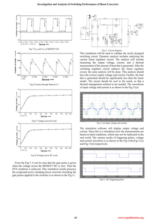
Fig.11. (c) Output current
Fig.11 (d) Output voltage
The purpose of this subcomponent is to take the input DC
voltage (either from a DC source e.g. power supply or battery,
or from the rectifier output) and convert the output to a
consistent 45Vdc. As the design considers that the input
voltage may vary somewhere between 40V and 50V, the
circuit must be able to both step-up and step-down the voltage
as necessary. This need implies the usage of a buck-boost
converter, which was originally proposed. The circuit
diagram for dc motor load is as shown in the Fig.12.
This has been changed since the design review into a fly
back converter, which operates equivalently save for several
differences. The buck-boost converter inverts the output (in
this case taking the positive input to a -45V output), which
was not desired. The fly back converter can both invert the
output or keep the sign unchanged, the output determined by
the polarity on the secondary winding. Also, the fly back
converter uses a coupled inductor in the design, which also
provides electrical isolation to the output, which while not
necessary may be beneficial in applications.
Fig.12.Circuit diagram for dc motor load
Fig.12 (a) Input voltage
Fig.12 (b), (c) DC Motor speed and torque output
Fig.13(c) Output current
VI. CONCLUSION
The operation of compound active clamping boost PFC
converter, the mathematical analysis of the step-up chopper
and the simulation results of the circuit are presented. A novel
interleaved boost converter with both zero-voltage switching
and zero-current-switching functions is proposed in this paper
the main switches can achieve both ZVS and ZCS. Thus we
designed a interleaved booster with reduces switching loses
and ripples of input current and output voltage. The voltage
stress of all switches is equal to the output voltage. It has the
smaller current stress of elements
REFERENCES
[1] P Evans and W Heffernan, “Inductor design concepts for high
frequency applications”, EPE FIRENZE, pp. 1.019-1-1.024, 2012.
[2] Guichao Hua and F C Lee, “Soft switching techniques in PWM
converters”, IEEE IECON, pp. 637-643, 2011.
[3] A W Zhang, M. T Zhang and F C Lee et al., “Conducted EMI analysis of
a boost PFC Circuit”, Proc. IEEE Applied Power Electronics conf.,
APEC – 2009, vol. 1.
[4] J C Crebier, M Brunello and J P Ferrieux, “A new method for EMI study
in PFC rectifiers”, Proc. IEEE Power Electronics Spc. Conf., PESC – 2011,
pp. 855-860.
[5] L. Rossetto, P. Tenti and A. Zucato, “Electromagnetic Compatibility
issue in industrial equipment”, IEEE Ind. Applications, Mag., pp. 34-36,
Nov / Dec. 2009.
[6] J. Qian and F.C. Lee, “Charge pump power factor correction
technologies part I and Part II”, IEEE Trans. Power Electronics, vol. 15, pp.
121-139, Jan. 2010.
[7] T. Ohnishi and M. Hojo, “Single phase PFC converter with switching
pulse free chopper”, Proc. IPEC – 2010, Tokyo, Japan, pp. 1796-1801,
2010.
6. Investigation and Analysis of Switching Performance of Boost Converter
43 www.erpublication.org
BIOGRAPHY
Dr.S.SANKAR obtained his B.E Degree in
Electrical & Electronics Engineering at Sri
Venkateswara College of Engineering, from
Madras University and M.E (Power System)
Degree from Annamalai University Chidambaram.
He has done his Ph.D in the area of FACTS
controllers in 2011. His research interests are in the
area of FACTS, Electrical Machines, Voltage
stability, power quality, Power system security and
Power System Analysis.
Mr.E.PARTHEEPAN is a Research Scholar in
St. peter’s University. His area of interest is Power
System Stability, Dynamics, Renewable Power
Generation, UPQC, FACTS, Hybrid Power
Generation & High Voltage Engineering. He
published various papers in International Journals
& Conferences.
Dr S.SARAVANAKUMAR has more than 10
years of teaching and research experience. He did
his Postgraduate in ME in Computer Science and
Engineering at Bharath engineering college,anna
university chennai, and Ph.D in Computer Science
and Engineering at Bharath University, Chennai.
He has guiding a number of research scholars in the
area Adhoc Network, ANN, Security in Sensor
Networks, Mobile Database and Data Mining
under Bharath University Chennai, , Sathayabama
University and Bharathiyar University.