Downloaded 535 times

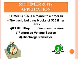
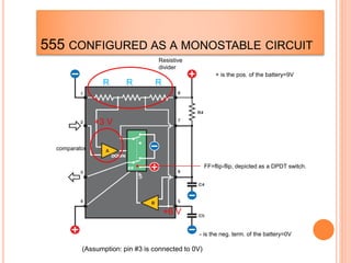
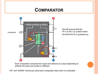
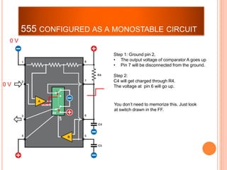
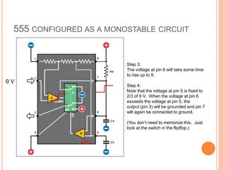
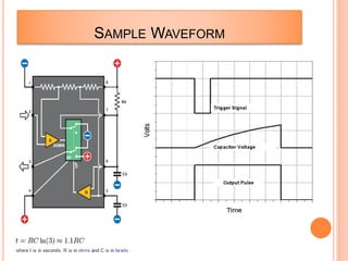
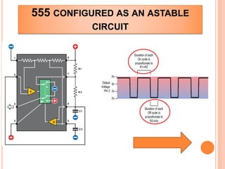
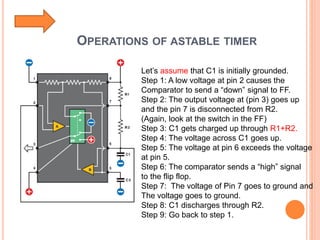
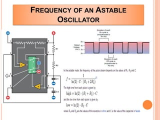
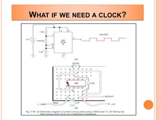
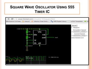
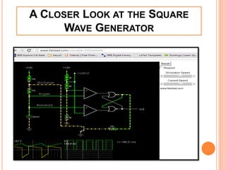
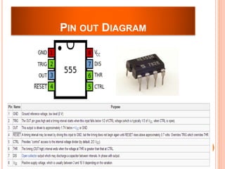


This presentation discusses the 555 timer IC and its applications in analog circuit design. It begins by describing the basic building blocks of the 555 timer IC, which include an RS flip-flop, two comparators, a reference voltage source, and a discharge transistor. It then shows how the 555 timer can be configured as a monostable and astable multivibrator. Diagrams illustrate the voltage levels and switching in each configuration. Sample waveforms are displayed and the operations of the astable timer circuit are explained in steps. Applications for a square wave oscillator and clock circuit using the 555 timer IC are also presented.