The document discusses silicon controlled rectifiers (SCRs). Key points:
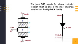
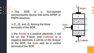
- SCRs are four-layer semiconductor devices that form an NPNP or PNPN structure with three terminals - anode, cathode, and gate.
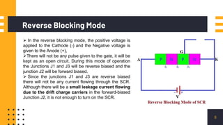
- SCRs can operate in forward blocking, forward conduction, or reverse blocking modes depending on voltage polarity and gate signal.
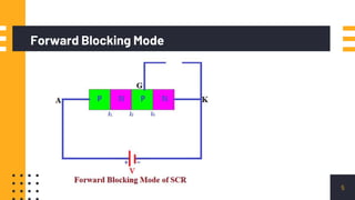
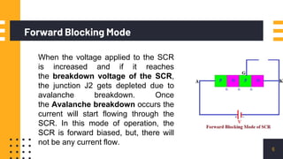
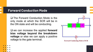
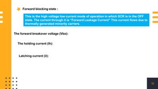
- Forward blocking mode allows voltage buildup but no current flow. Forward conduction occurs when voltage exceeds the breakdown voltage or gate is pulsed.
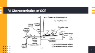
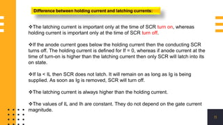
- Characteristics include forward breakover voltage, holding current, and latching current. Holding current maintains conduction; latching current triggers the device.
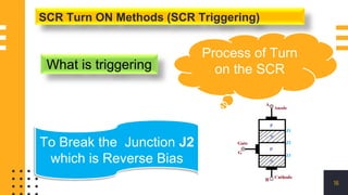
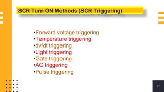
- SCRs can be triggered