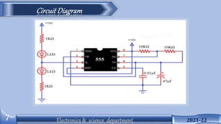
ORIENTAL COLLEGE OF
TECHNOLOGY
555TIMERICTESTINGCIRCUIT
Minor Project
Progress Presentation I
Electronics & Communication
B-TECH, 5-SEM
1 2021-22
Chetan Borban (0126EC191019)
Nitish Singh (0126EC191036)
Shobhit Singh(0126EC101953)
Vidya S. Singh(012EC101958)
Saarthak Lakhani(0126EC191047)
Piyush Jain
2021-22
2
I. About Project
II. Objective
III. Required Components
IV. Description on component
V. Circuit Diagram & Pin Diagram
VI. About Methodology
VII. Application / uses this Circuit
VIII. Work Plan
IX. Reference
The 555 Timer IC is one of the most popular and
most frequently used integrated circuits. It performs
an array of timing tasks in the electronic circuits. But
before using the 555 Timer IC, check it’s whether, it
is working properly or not.
3 2021-22
So, we are design a simple circuit that can be used
as a 555 Timer IC Testing Circuit and determine
whether the 555 IC is functioning or not.
Our objective is very clear, We are making a basic circuit with
help the of (active and passive ) components/elements which
help the testing 555 timer IC.
555 Timer IC is that it has three modes of operation: Astable,
Monostable and Bistable. The circuit implemented in this
project is basically an Astable Mode of operation of the 555
Timer IC.
4 2021-22
 555 IC
 2 X 10KΩ Resistors
 2 X 1KΩ Resistors
 47μF Capacitor (Electrolytic)
 0.01μF Capacitor (Ceramic Disc)
 2 X LEDs
 12V Power Supply
5 2021-22
6 2021-22
We are using
two type
Resistor. 2*1KΩ
and 2*10Ω, 1KΩ
using for ‘LED’
and 10KΩ using
for IC.
We are using
two type
capacitor. 47μF
(Electrolytic)
and 0.01μF
(Ceramic Disc)
for voltage
control.
We are using
two LED light for
indication.
We should 5V to
12V power for our
circuit, So we can
use 9V power
supply.
Ex: - Battery,
Mobile Charger
etc.
555 Timer IC is main element/ component of
our project.
It have 8-PIN, Dual-in-line Package (DIP).
The 555 timer can be operated at a wide range
of power supplies ranging from 5 V to 18 V.
7 2021-22
PIN-1
Ground reference voltage (low level
0V). All the voltages are measured
with respect to this terminal.
PIN-2
It is responsible for SET and RESET
transitions of the flip-flop.
PIN-3
Output driven waveform is available
at this pin. It is driven to 1.7 V below
VCC. Two types of loads can be
connected to the output.
PIN-4
A negative pulse on this pin will disable
or reset the timer. The timer will begin
only when the voltage on this pin is
above 0.7 V and hence it is normally
connected to VCC when not used.
PIN-5
It controls the threshold and trigger
levels and hence the timing of the
555. The width of the output pulse is
determined by the control voltage.
PIN-6
The voltage applied at this terminal is
compared with a reference voltage of
2/3 VCC. When the voltage at this
terminal is greater than 2/3 VCC, the
flip-flop is RESET and the output falls
from High to Low.
PIN-7
It is connected to the open collector of the
internal NPN transistor which discharges
the timing capacitor. When the voltage at
this pin reaches 2/3 VCC, the output
toggles from high to low.
PIN-8
A supply voltage in the range of 5V
to 18V is applied to this terminal.
8 2021-22
9 2021-22
In this circuit, We have used the 555 IC as an Astable multivibrator and when
power is provided to circuit, the LEDs will start blinking, which means that the IC
is working. The blinking rate of LEDs can be changed by increasing or
decreasing the values of resistor R1 and R2 and capacitor C1.
Formula
ON Time (HIGH) in Seconds = 0.693 * (R1
+ R2) * C1
OFF Time (LOW) in Seconds = 0.693 * R2 *
C1
Total Time Period in Seconds = 0.693 * (R1
+2R2)*C1
Frequency = 1.44 / ((R1 + 2R2) * C1)
Accordingour circuit(Resistors,Capacitorsand Power
Supply.)
Frequency = 1.023 Hertz
ON Time = 0.651 Seconds
OFF Time = 0.326 Seconds
Time Period = 0.977 Seconds
1 0 2021-22
Case-1
Now to see the result, switch on the
power supply. If our 555 Timer IC is
working properly, then both the
LEDs (Red LEDs in my case) will
glow alternately.
Case-2
If any of the LED is OFF or both the
LEDs are not glowing, it means that
our 555 timer IC is faulty.
We will receive two different
types
of Case
1 1 2021-22
 Square Wave Generation
 Pulse Position Modulation
 Pulse Train
 Frequency Modulation using Astable Multivibrator
Note: - our 555 testing IC circuit is used in this application
1 2 2021-22
S. NO. PARTICUAL DURATION OUTCOME
1
Literature Survey
20-Sep-2021
Study about the 555 Timer IC
Testing circuit
2 Components Identification 26-Sep-2021
Identify Components to be
required in project
3
Layout Plane/ Circuit
Diagram
02-Oct-2021
Design of layout of electronics
circuit
4 Assembler Components 05-Oct-2021
Purchase Components form
Market.
5 Progress Presentation-1 11-Oct-2021
Represent project details in ppt
and report.
1 3 2021-22
About 555 Timer IC: -
From: - Tutorialspoint.com
From:- CircuitsToday.com
Project Idea
From: - CircuitsToday.com
PCB Design and simulation
From: - CircuitLab.com

555 timer ic_tesitngcircuit

  • 1.
    ORIENTAL COLLEGE OF TECHNOLOGY 555TIMERICTESTINGCIRCUIT MinorProject Progress Presentation I Electronics & Communication B-TECH, 5-SEM 1 2021-22 Chetan Borban (0126EC191019) Nitish Singh (0126EC191036) Shobhit Singh(0126EC101953) Vidya S. Singh(012EC101958) Saarthak Lakhani(0126EC191047) Piyush Jain
  • 2.
    2021-22 2 I. About Project II.Objective III. Required Components IV. Description on component V. Circuit Diagram & Pin Diagram VI. About Methodology VII. Application / uses this Circuit VIII. Work Plan IX. Reference
  • 3.
    The 555 TimerIC is one of the most popular and most frequently used integrated circuits. It performs an array of timing tasks in the electronic circuits. But before using the 555 Timer IC, check it’s whether, it is working properly or not. 3 2021-22 So, we are design a simple circuit that can be used as a 555 Timer IC Testing Circuit and determine whether the 555 IC is functioning or not.
  • 4.
    Our objective isvery clear, We are making a basic circuit with help the of (active and passive ) components/elements which help the testing 555 timer IC. 555 Timer IC is that it has three modes of operation: Astable, Monostable and Bistable. The circuit implemented in this project is basically an Astable Mode of operation of the 555 Timer IC. 4 2021-22
  • 5.
     555 IC 2 X 10KΩ Resistors  2 X 1KΩ Resistors  47μF Capacitor (Electrolytic)  0.01μF Capacitor (Ceramic Disc)  2 X LEDs  12V Power Supply 5 2021-22
  • 6.
    6 2021-22 We areusing two type Resistor. 2*1KΩ and 2*10Ω, 1KΩ using for ‘LED’ and 10KΩ using for IC. We are using two type capacitor. 47μF (Electrolytic) and 0.01μF (Ceramic Disc) for voltage control. We are using two LED light for indication. We should 5V to 12V power for our circuit, So we can use 9V power supply. Ex: - Battery, Mobile Charger etc. 555 Timer IC is main element/ component of our project. It have 8-PIN, Dual-in-line Package (DIP). The 555 timer can be operated at a wide range of power supplies ranging from 5 V to 18 V.
  • 7.
  • 8.
    PIN-1 Ground reference voltage(low level 0V). All the voltages are measured with respect to this terminal. PIN-2 It is responsible for SET and RESET transitions of the flip-flop. PIN-3 Output driven waveform is available at this pin. It is driven to 1.7 V below VCC. Two types of loads can be connected to the output. PIN-4 A negative pulse on this pin will disable or reset the timer. The timer will begin only when the voltage on this pin is above 0.7 V and hence it is normally connected to VCC when not used. PIN-5 It controls the threshold and trigger levels and hence the timing of the 555. The width of the output pulse is determined by the control voltage. PIN-6 The voltage applied at this terminal is compared with a reference voltage of 2/3 VCC. When the voltage at this terminal is greater than 2/3 VCC, the flip-flop is RESET and the output falls from High to Low. PIN-7 It is connected to the open collector of the internal NPN transistor which discharges the timing capacitor. When the voltage at this pin reaches 2/3 VCC, the output toggles from high to low. PIN-8 A supply voltage in the range of 5V to 18V is applied to this terminal. 8 2021-22
  • 9.
    9 2021-22 In thiscircuit, We have used the 555 IC as an Astable multivibrator and when power is provided to circuit, the LEDs will start blinking, which means that the IC is working. The blinking rate of LEDs can be changed by increasing or decreasing the values of resistor R1 and R2 and capacitor C1. Formula ON Time (HIGH) in Seconds = 0.693 * (R1 + R2) * C1 OFF Time (LOW) in Seconds = 0.693 * R2 * C1 Total Time Period in Seconds = 0.693 * (R1 +2R2)*C1 Frequency = 1.44 / ((R1 + 2R2) * C1) Accordingour circuit(Resistors,Capacitorsand Power Supply.) Frequency = 1.023 Hertz ON Time = 0.651 Seconds OFF Time = 0.326 Seconds Time Period = 0.977 Seconds
  • 10.
    1 0 2021-22 Case-1 Nowto see the result, switch on the power supply. If our 555 Timer IC is working properly, then both the LEDs (Red LEDs in my case) will glow alternately. Case-2 If any of the LED is OFF or both the LEDs are not glowing, it means that our 555 timer IC is faulty. We will receive two different types of Case
  • 11.
    1 1 2021-22 Square Wave Generation  Pulse Position Modulation  Pulse Train  Frequency Modulation using Astable Multivibrator Note: - our 555 testing IC circuit is used in this application
  • 12.
    1 2 2021-22 S.NO. PARTICUAL DURATION OUTCOME 1 Literature Survey 20-Sep-2021 Study about the 555 Timer IC Testing circuit 2 Components Identification 26-Sep-2021 Identify Components to be required in project 3 Layout Plane/ Circuit Diagram 02-Oct-2021 Design of layout of electronics circuit 4 Assembler Components 05-Oct-2021 Purchase Components form Market. 5 Progress Presentation-1 11-Oct-2021 Represent project details in ppt and report.
  • 13.
    1 3 2021-22 About555 Timer IC: - From: - Tutorialspoint.com From:- CircuitsToday.com Project Idea From: - CircuitsToday.com PCB Design and simulation From: - CircuitLab.com