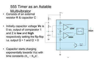
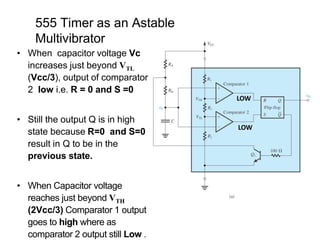
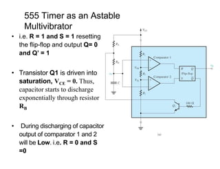
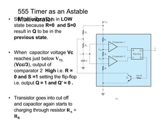
Download to read offline
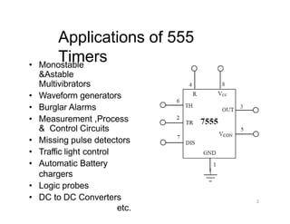
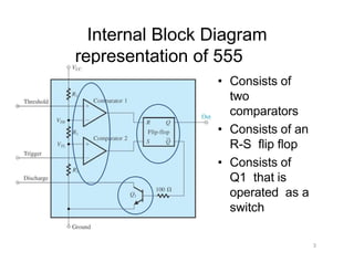


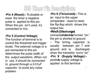
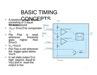
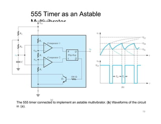

The document describes various applications of the 555 timer integrated circuit including waveform generation, burglar alarms, and traffic light control. It provides details on the internal components of the 555 timer including two comparators and an R-S flip-flop. Circuit diagrams and explanations are given for using the 555 timer as both a monostable and astable multivibrator, with derivations of timing equations. Key voltage thresholds and the states of internal components are indicated in diagrams showing the charging and discharging operation of the timer circuits.