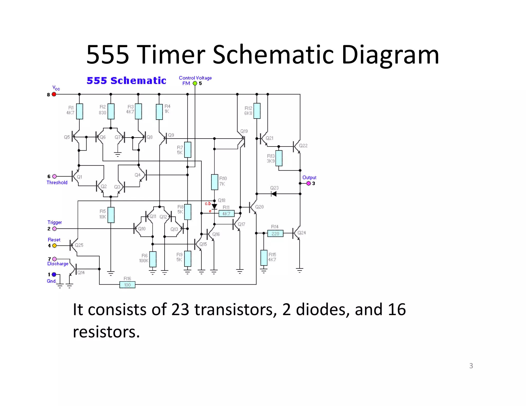
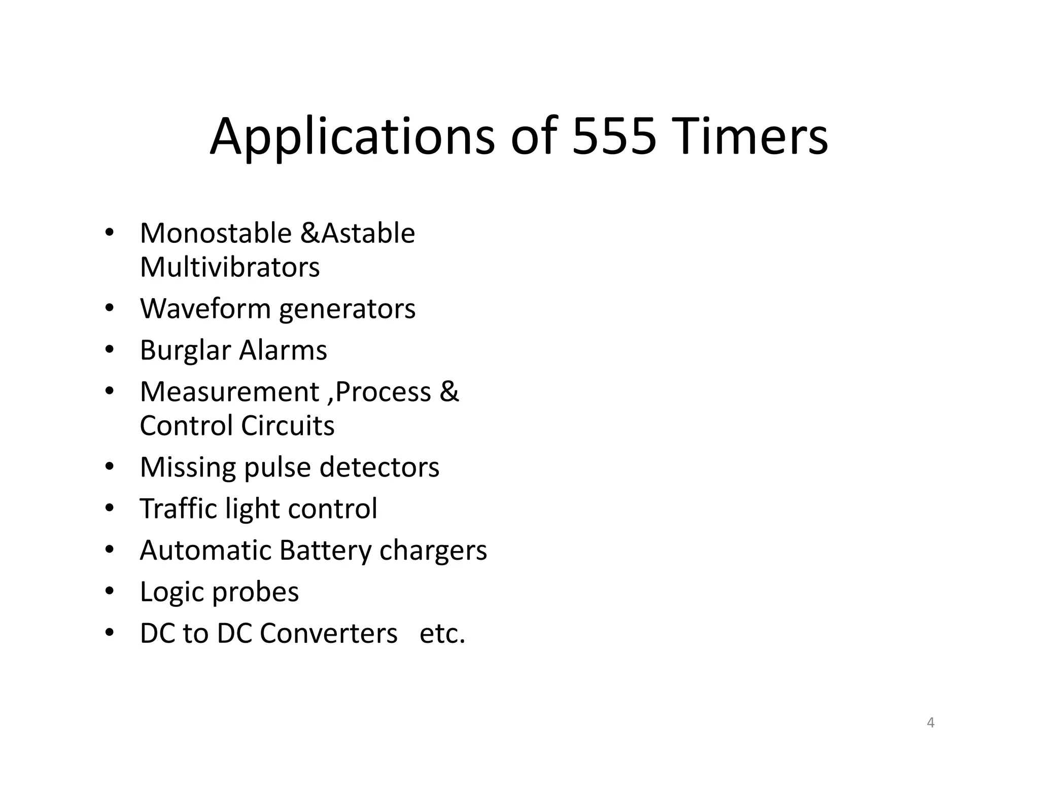
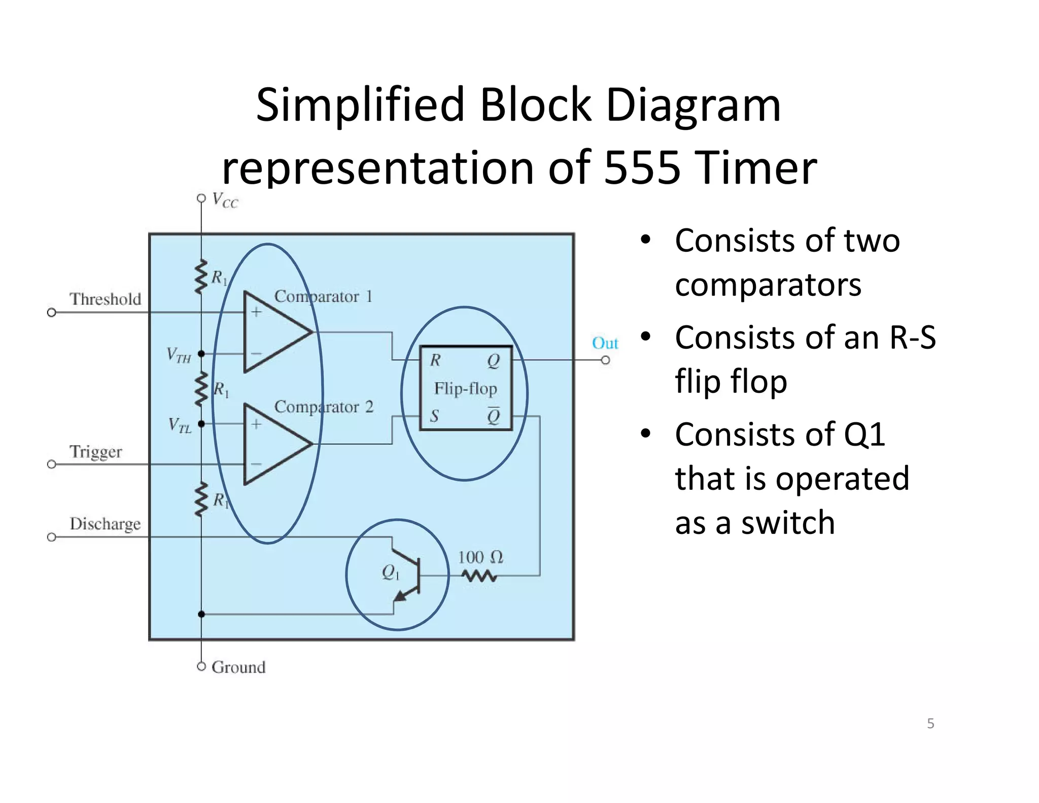
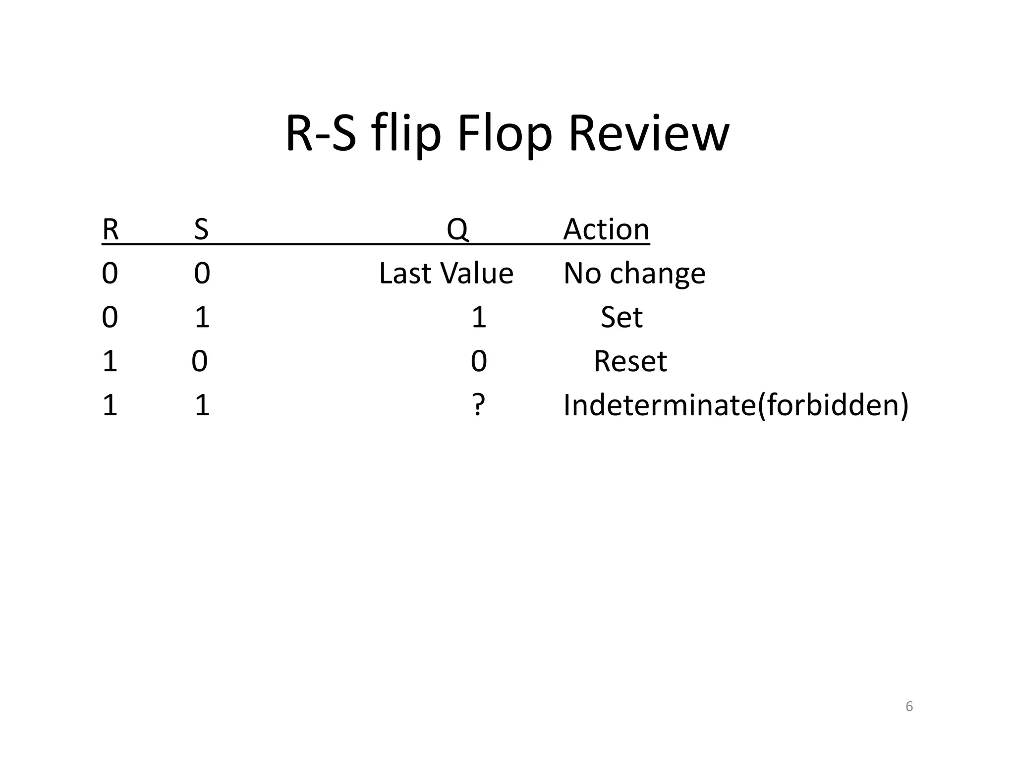
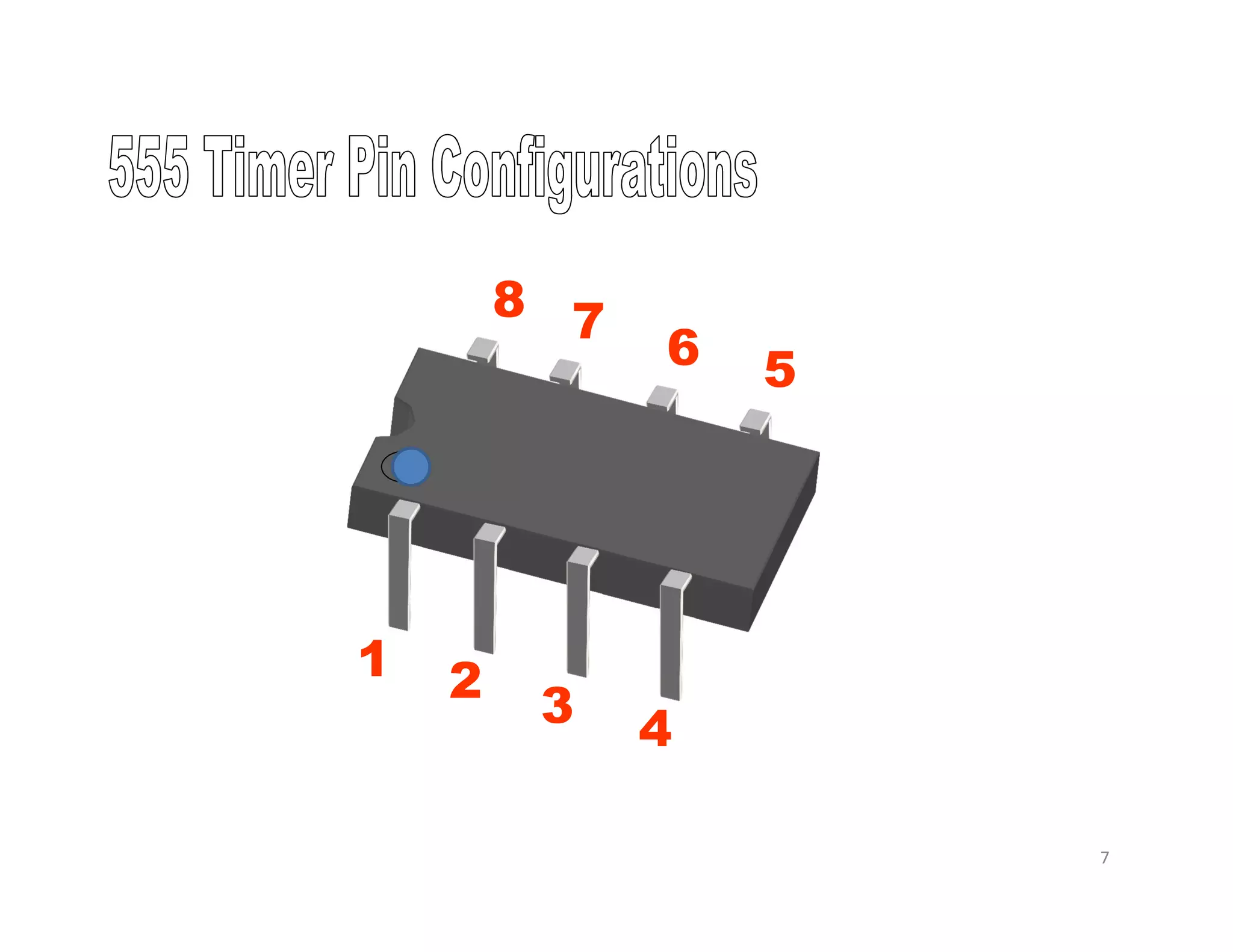
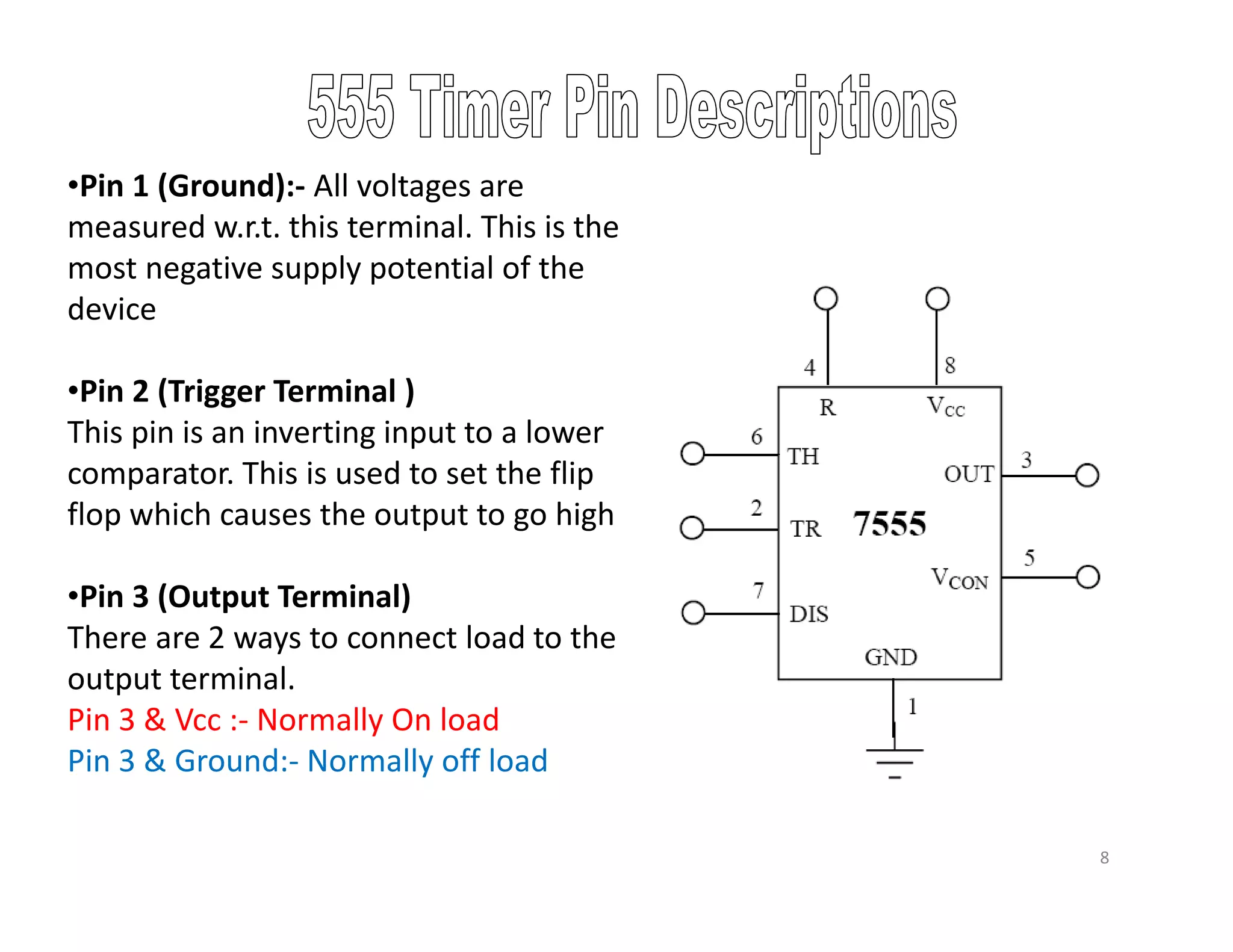
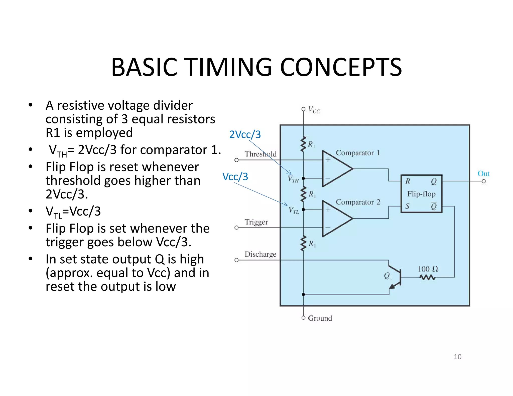
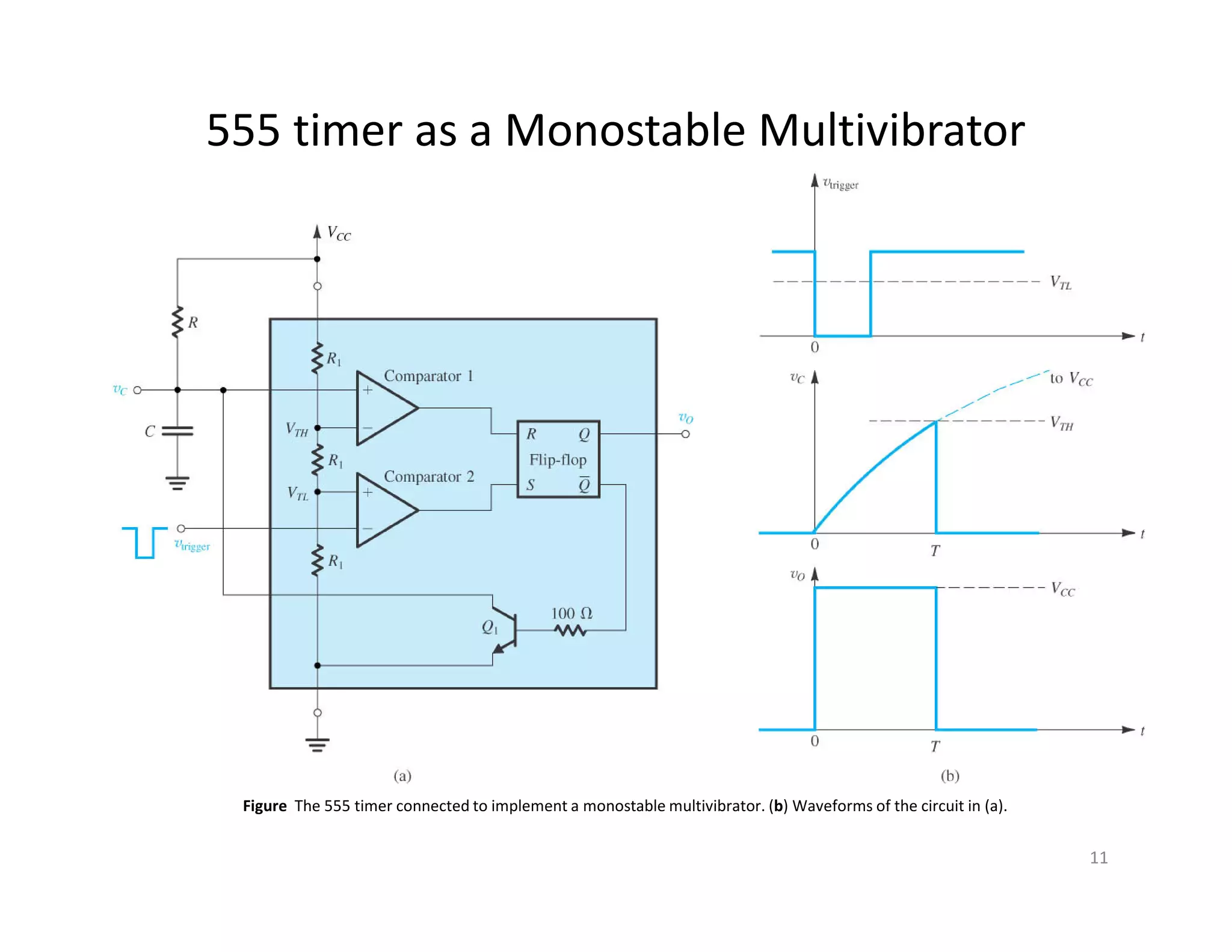
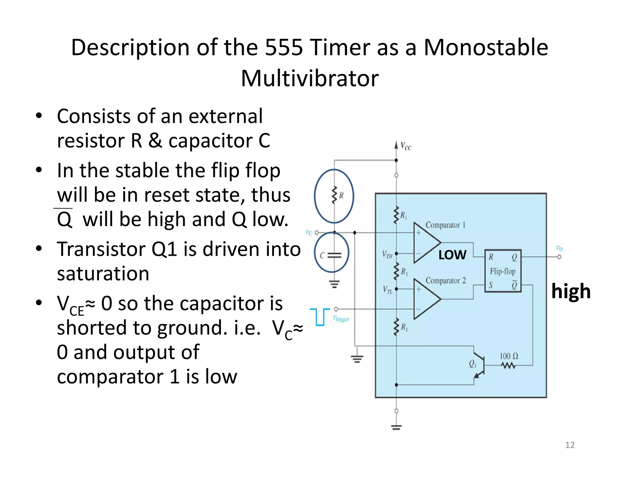
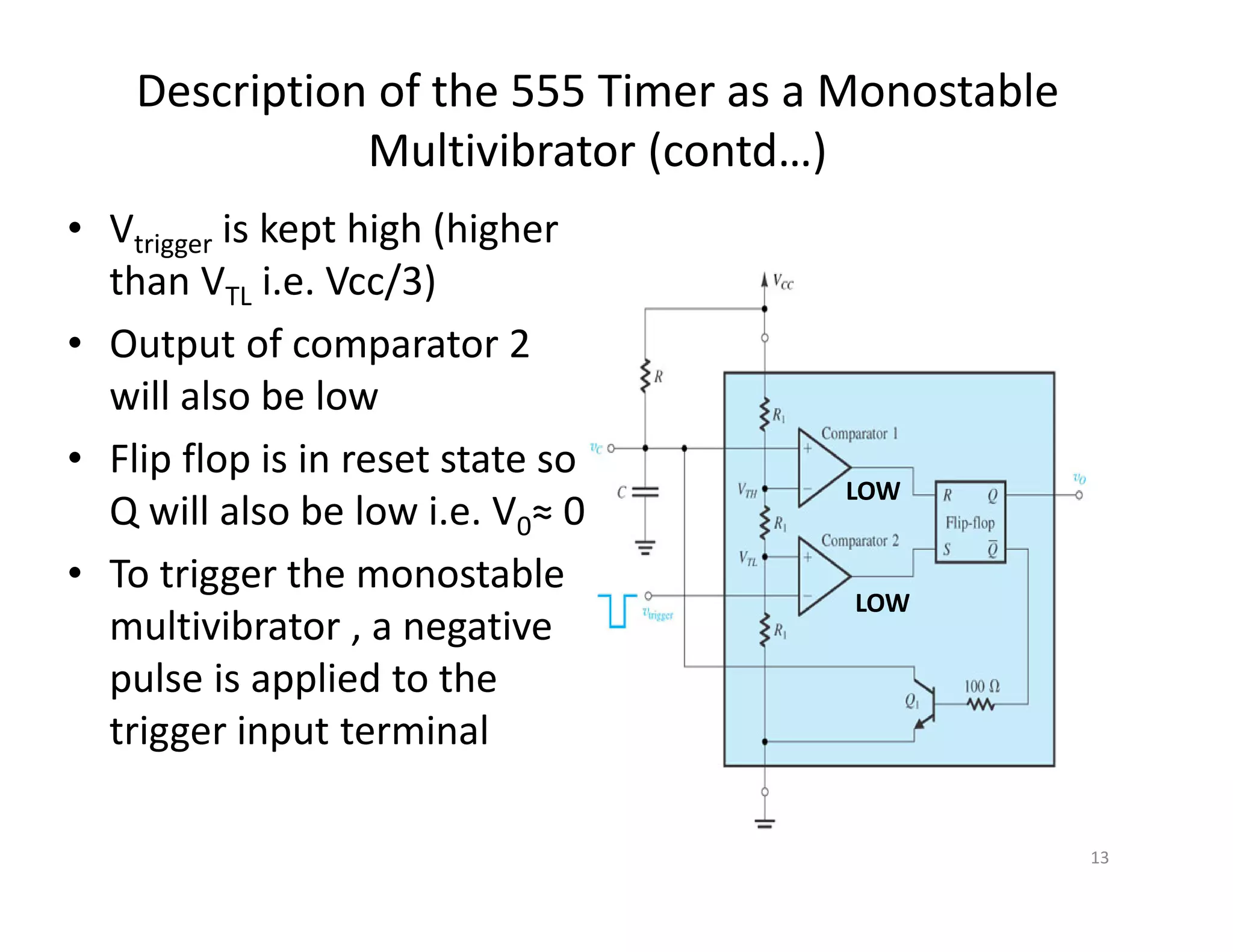
The 555 timer IC was introduced in 1971 by Signetics Corporation. It provided an inexpensive and stable integrated circuit for monostable and astable applications. It consists of 23 transistors, 2 diodes, and 16 resistors. As a monostable multivibrator, it produces a single pulse when triggered, with the pulse width determined by the external resistor and capacitor. As an astable multivibrator, it continuously switches its output between high and low without an external trigger, with the pulse width set by two external resistors and one capacitor. The 555 timer has found applications in waveform generation, timers, oscillators, and more due to its low cost and ease of use.
PowerPoint Presentation on using IC 555 Timer as an Astable Multi vibrator. Working of the astable multi vibrator, advantages and disadvantages of an Astable Multi-vibrator,Input and Output Pins of 555 IC, Formulae for calculating the charge and discharge time and cycle time of the astable multi vibrator.
1.Introduction
The 555 IC was designed in 1971 by Hans Camenzind under contract to SigNetics Corporation.
555 timer is a highly stable circuit used to generate time delays, or Oscillations.
A single 555 timer can provide time delay ranging from microseconds to hours.
It operates from a wide range of power supplies ranging from + 5 Volts to + 18 Volts supply voltage.
2.Pin Configuration
3.Working of Pin
4.555 Integral circuit
5.Operating modes of IC
6. Bistable Mode
In bistable (also called Schmitt trigger) mode, the 555 timer acts as a basic flip-flop.
The trigger and reset inputs (pins 2 and 4 respectively on a 555) are held high via pull-up resistors while the threshold input (pin 6) is simply floating.
Thus configured, pulling the trigger momentarily to ground acts as a 'set' and transitions the output pin (pin 3) to Vcc (high state).
Pulling the reset input to ground acts as a 'reset' and transitions the output pin to ground (low state). No timing capacitors
Pin 5 (control voltage) is connected to ground via a small-value capacitor (usually 0.01 to 0.1 μF). Pin 7 (discharge) is left floating
7.Monostable Mode
Pulse generator circuit which the period is calculated from RC network and connected to external of 555 timer
Stable when the output logic LOW (logic = 0)
When a pulse is trigger at pin 2 (normally negative trigger pulse), timer output will change to HIGH (+Vs) for a while and change to LOW (stable condition). The condition will continue LOW until pulse is trigger again.
The timing period is triggered (started) when trigger input (555 pin 2) is less than 1/3 Vs, this makes the output high (+Vs) and the capacitor C1 starts to charge through resistor R1. Once the time period has started further trigger pulses are ignored.
The threshold input (555 pin 6) monitors the voltage across C1 and when this reaches 2/3 Vs the time period over and the output becomes LOW,
At the same time discharge (555 pin 7) is connected to 0V, discharging the capacitor ready for the next trigger.
8.Astable Mode
Astable multivibrators are also known as Free-running Multivibrator.
Astable do not need trigger pulse for external to change the output.
The period for LOW and HIGH can be calculated based on resistor and capacitor value that connected at outside of timer.
9.Applications
Schmitt trigger
PPM
PWM
Linear Ramp generator
Precision Timing
Pulse Generation
Time Delay Generation
Sequential Timing
Used as a quad timer
10. Conclusion
Hence 555 IC timer can produce very accurate and stable time delays, from microseconds to hours. It can be used with supply voltage varying from 5 to 18 V. Timer can be used in monostable mode of operation or astable mode of operation. Its various applications include waveform generator, missing pulse detector, frequency divider, pulse width modulator, burglar alarm, FSK generator, ramp generator, pulse position modulator etc.
Functional block, characteristics of 555 Timer and its PWM application – IC-566 voltage controlled oscillator IC; 565-phase locked loop IC, AD633 Analog multiplier ICs.
IC 555 TIMER Introduction, Modes & Application.pptxanindyapal288
Pin 1. – Ground, The ground pin connects the 555 timer to the negative (0v) supply rail.
• Pin 2. – Trigger, The negative input to comparator No 1. A negative pulse on this pin “sets” the internal Flip-flop when the voltage drops below 1/3Vcc causing the output to switch from a “LOW” to a “HIGH” state.
• Pin 3. – Output, The output pin can drive any TTL circuit and is capable of sourcing or sinking up to 200mA of current at an output voltage equal to approximately Vcc – 1.5V so small speakers, LEDs or motors can be connected directly to the output.
• Pin 4. – Reset, This pin is used to “reset” the internal Flip-flop controlling the state of the output, pin 3. This is an active-low input and is generally connected to a logic “1” level when not used to prevent any unwanted resetting of the output.
• Pin 5. – Control Voltage, This pin controls the timing of the 555 by overriding the 2/3Vcc level of the voltage divider network. By applying a voltage to this pin the width of the output signal can be varied independently of the RC timing network. When not used it is connected to ground via a 10nF capacitor to eliminate any noise.
• Pin 6. – Threshold, The positive input to comparator No 2. This pin is used to reset the Flip-flop when the voltage applied to it exceeds 2/3Vcc causing the output to switch from “HIGH” to “LOW” state. This pin connects directly to the RC timing circuit.
• Pin 7. – Discharge, The discharge pin is connected directly to the Collector of an internal NPN transistor which is used to “discharge” the timing capacitor to ground when the output at pin 3 switches “LOW”.
• Pin 8. – Supply +Vcc, This is the power supply pin and for general purpose TTL 555 timers is between 4.5V and 15V.
SIMULATION OF AN ELECTRONIC DICE CIRCUIT USING LEDs IN PROTEUS SOFTWARE VaishaliVaishali14
The following content consists of the brief details about the topic
INTRODUCTION
CONCEPT OF ASTABLE MULTI VIBRATOR
CONCEPT OF DECADE COUNTER IC4017
CIRCUIT EXPLANATION
CIRCUIT DIAGRAM
VIDEO OF CIRCUIT WORKING
WORKING OF CIRCUIT
INFERENCE
REFERENCE
Simple Automatic Water Level Controller by using ic 555 timer.PRASHANTH RAO
It is a very simple project.present situation all are facing water problems.to over come that water wasteges we are made this project.It is very easy to do and low cost.the cost in between 200 to 300.without human involving it will work.
IC555 Timer, Monostable and Astable modes of operation; voltage regulators - fixed voltage regulators, adjustable voltage regulators - switching regulators.
Linear Integrated Circuits and Its Applications Unit-V Special ICsSatheeshCS2
Linear Integrated Circuits and Its Applications
Unit-V Special ICs
Mr. C.S.SATHEESH, M.E.(Control Systems),
Assistant Professor, Department of EEE, Muthayammal Engineering College, (Autonomous) Namakkal (Dt), Rasipuram – 637408
A brief information about the SCOP protein database used in bioinformatics.
The Structural Classification of Proteins (SCOP) database is a comprehensive and authoritative resource for the structural and evolutionary relationships of proteins. It provides a detailed and curated classification of protein structures, grouping them into families, superfamilies, and folds based on their structural and sequence similarities.
What is greenhouse gasses and how many gasses are there to affect the Earth.moosaasad1975
What are greenhouse gasses how they affect the earth and its environment what is the future of the environment and earth how the weather and the climate effects.
(May 29th, 2024) Advancements in Intravital Microscopy- Insights for Preclini...Scintica Instrumentation
Intravital microscopy (IVM) is a powerful tool utilized to study cellular behavior over time and space in vivo. Much of our understanding of cell biology has been accomplished using various in vitro and ex vivo methods; however, these studies do not necessarily reflect the natural dynamics of biological processes. Unlike traditional cell culture or fixed tissue imaging, IVM allows for the ultra-fast high-resolution imaging of cellular processes over time and space and were studied in its natural environment. Real-time visualization of biological processes in the context of an intact organism helps maintain physiological relevance and provide insights into the progression of disease, response to treatments or developmental processes.
In this webinar we give an overview of advanced applications of the IVM system in preclinical research. IVIM technology is a provider of all-in-one intravital microscopy systems and solutions optimized for in vivo imaging of live animal models at sub-micron resolution. The system’s unique features and user-friendly software enables researchers to probe fast dynamic biological processes such as immune cell tracking, cell-cell interaction as well as vascularization and tumor metastasis with exceptional detail. This webinar will also give an overview of IVM being utilized in drug development, offering a view into the intricate interaction between drugs/nanoparticles and tissues in vivo and allows for the evaluation of therapeutic intervention in a variety of tissues and organs. This interdisciplinary collaboration continues to drive the advancements of novel therapeutic strategies.
Professional air quality monitoring systems provide immediate, on-site data for analysis, compliance, and decision-making.
Monitor common gases, weather parameters, particulates.
Cancer cell metabolism: special Reference to Lactate PathwayAADYARAJPANDEY1
Normal Cell Metabolism:
Cellular respiration describes the series of steps that cells use to break down sugar and other chemicals to get the energy we need to function.
Energy is stored in the bonds of glucose and when glucose is broken down, much of that energy is released.
Cell utilize energy in the form of ATP.
The first step of respiration is called glycolysis. In a series of steps, glycolysis breaks glucose into two smaller molecules - a chemical called pyruvate. A small amount of ATP is formed during this process.
Most healthy cells continue the breakdown in a second process, called the Kreb's cycle. The Kreb's cycle allows cells to “burn” the pyruvates made in glycolysis to get more ATP.
The last step in the breakdown of glucose is called oxidative phosphorylation (Ox-Phos).
It takes place in specialized cell structures called mitochondria. This process produces a large amount of ATP. Importantly, cells need oxygen to complete oxidative phosphorylation.
If a cell completes only glycolysis, only 2 molecules of ATP are made per glucose. However, if the cell completes the entire respiration process (glycolysis - Kreb's - oxidative phosphorylation), about 36 molecules of ATP are created, giving it much more energy to use.
IN CANCER CELL:
Unlike healthy cells that "burn" the entire molecule of sugar to capture a large amount of energy as ATP, cancer cells are wasteful.
Cancer cells only partially break down sugar molecules. They overuse the first step of respiration, glycolysis. They frequently do not complete the second step, oxidative phosphorylation.
This results in only 2 molecules of ATP per each glucose molecule instead of the 36 or so ATPs healthy cells gain. As a result, cancer cells need to use a lot more sugar molecules to get enough energy to survive.
introduction to WARBERG PHENOMENA:
WARBURG EFFECT Usually, cancer cells are highly glycolytic (glucose addiction) and take up more glucose than do normal cells from outside.
Otto Heinrich Warburg (; 8 October 1883 – 1 August 1970) In 1931 was awarded the Nobel Prize in Physiology for his "discovery of the nature and mode of action of the respiratory enzyme.
WARNBURG EFFECT : cancer cells under aerobic (well-oxygenated) conditions to metabolize glucose to lactate (aerobic glycolysis) is known as the Warburg effect. Warburg made the observation that tumor slices consume glucose and secrete lactate at a higher rate than normal tissues.
Comparing Evolved Extractive Text Summary Scores of Bidirectional Encoder Rep...University of Maribor
Slides from:
11th International Conference on Electrical, Electronics and Computer Engineering (IcETRAN), Niš, 3-6 June 2024
Track: Artificial Intelligence
https://www.etran.rs/2024/en/home-english/
1. 555 TIMER IC HISTORY
• The 555 timer IC was first introduced around 1971 by the
Signetics Corporation as the SE555/NE555
• Initially it was called "The IC Time Machine"
• It provided circuit designers with a relatively cheap, stable, and
user-friendly integrated circuit for both monostable and
astable applications.
• Since this device was first made commercially available, a
multitude of novel and unique circuits have been developed
• The past ten years some manufacturers stopped making these
timers
• Yet other companies, like NTE (a subdivision of Philips) picked
up where some left off
2
2. 555 Timer Schematic Diagram
It consists of 23 transistors, 2 diodes, and 16
resistors.
3
3. Applications of 555 Timers
• Monostable &Astable
Multivibrators
• Waveform generators
• Burglar Alarms
• Measurement ,Process &
Control Circuits
• Missing pulse detectors
• Traffic light control
• Automatic Battery chargers
• Logic probes
• DC to DC Converters etc.
4
4. Simplified Block Diagram
representation of 555 Timer
• Consists of two
comparators
• Consists of an R-S
flip flop
• Consists of Q1
that is operated
as a switch
5
5. R-S flip Flop Review
R S Q Action
0 0 Last Value No change
0 1 1 Set
1 0 0 Reset
1 1 ? Indeterminate(forbidden)
6
7. •Pin 1 (Ground):- All voltages are
measured w.r.t. this terminal. This is the
most negative supply potential of the
device
•Pin 2 (Trigger Terminal )
This pin is an inverting input to a lower
comparator. This is used to set the flip
flop which causes the output to go high
•Pin 3 (Output Terminal)
There are 2 ways to connect load to the
output terminal.
Pin 3 & Vcc :- Normally On load
Pin 3 & Ground:- Normally off load
8
8. •Pin 4 (Reset):- To disable or reset
the timer a negative pulse is
applied to this pin. When this pin
isn’t used, it’s connected to Vcc.
Why ??
•Pin 5 (Control Voltage)
The function of terminal is to
control the threshold and trigger
levels. The external voltage or a
pot connected to this pin
determines the pulse width of the
output waveform. When not in
use, it should be connected to
ground through a 0.01uF capacitor
to avoid any noise problem.
9
•Pin 6 (Threshold):- This is an
input to the upper comparator.
Used to reset the flip-flop which
drives the output low.
•Pin 7 (Discharge)
-When the npn transistor
connected to it is turned “on,”
the pin is shorted to ground
– The timing capacitor is usually
between pin 7 and ground and is
discharged when the transistor
turns “on”
•Pin 8 (Supply Voltage):- A
positive supply voltage is applied
to this terminal
9. BASIC TIMING CONCEPTS
• A resistive voltage divider
consisting of 3 equal resistors
R1 is employed
• VTH= 2Vcc/3 for comparator 1.
• Flip Flop is reset whenever
threshold goes higher than
2Vcc/3.
• VTL=Vcc/3
• Flip Flop is set whenever the
trigger goes below Vcc/3.
• In set state output Q is high
(approx. equal to Vcc) and in
reset the output is low
10
2Vcc/3
Vcc/3
10. 555 timer as a Monostable Multivibrator
11
Figure The 555 timer connected to implement a monostable multivibrator. (b) Waveforms of the circuit in (a).
11. Description of the 555 Timer as a Monostable
Multivibrator
• Consists of an external
resistor R & capacitor C
• In the stable the flip flop
will be in reset state, thus
Q will be high and Q low.
• Transistor Q1 is driven into
saturation
• VCE≈ 0 so the capacitor is
shorted to ground. i.e. VC≈
0 and output of
comparator 1 is low
12
high
LOW
12. Description of the 555 Timer as a Monostable
Multivibrator (contd…)
• Vtrigger is kept high (higher
than VTL i.e. Vcc/3)
• Output of comparator 2
will also be low
• Flip flop is in reset state so
Q will also be low i.e. V0≈ 0
• To trigger the monostable
multivibrator , a negative
pulse is applied to the
trigger input terminal
13
LOW
LOW
13. Description of the 555 Timer as a Monostable
Multivibrator (contd…)
• As Vtrigger goes below VTL i.e. Vcc/3,
the output of comparator 2 goes
high thus setting the flip flop. i.e.
Q=1 Q =0, so the transistor is
cutoff
• Vtrigger is given for a short time so
output of compartor 2 goes low
again.
• Still the ouput is high because R=0
and S=0 result in Q to be in the
previous state.
• Capacitor C now begins to charge
through resistor R and Vc rises
exponentially towards Vcc.
• The high voltage at the ouput is
retained as long as Vc<VTH
14
LOW
LOW
HIGH
HIGH
LOW
LOW
14. Description of the 555 Timer as a Monostable
Multivibrator (contd…)
• Once Vc exceeds VTH , the
output of comparator 1
goes high. Now R=1 and
S=0 so Q=0
• The monostable
multivibrator is now back
in its stable state and is
ready to receive a new
triggering pulse
15
LOW
LOW
HIGH
HIGH
HIGH LOW
15. Derivation for the width of the pulse in
monostable multivibrator
• The width of the pulse , T is the
time interval that the monostable
multivibrator spends in quasi
stable state.
• Denoting the time instant at
which the trigger pulse is applied
at t=0 , the voltage across
capacitor Vc can be expressed as ,
16
• Substituting Vc=VTH=2/3Vcc
at t=T gives,
T=RC ln 3 =1.1 RC
16. Figure 13.28 (a) The 555 timer connected to implement a monostable multivibrator. (b) Waveforms of the circuit in (a).
17
17. 555 Timer as an Astable Multivibrator
18
The 555 timer connected to implement an astable multivibrator. (b) Waveforms of the circuit in (a).