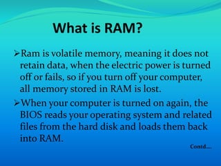
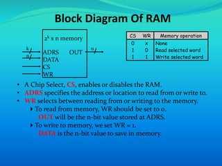
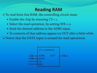
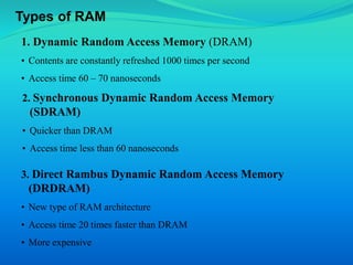
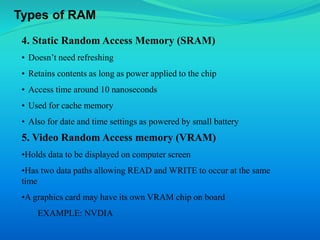
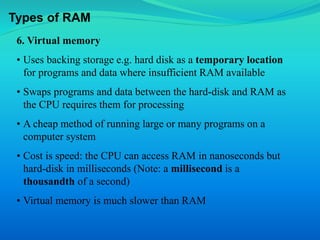
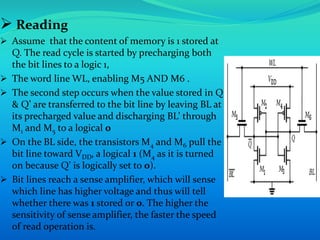
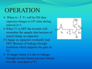
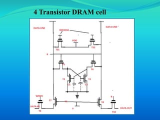
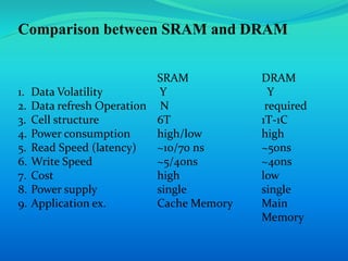
CONTENTS 
What is RAM ? 
Block diagram of Ram. 
Types of RAM. 
SRAM design & Operation. 
DRAM operation. 
Summary.
What is RAM? 
Ram is volatile memory, meaning it does not 
retain data, when the electric power is turned 
off or fails, so if you turn off your computer, 
all memory stored in RAM is lost. 
When your computer is turned on again, the 
BIOS reads your operating system and related 
files from the hard disk and loads them back 
into RAM. 
Contd….
RAM stores its data in a series of memory 
cells that can be accessed in any order, thus 
why it is called Random. 
SAM (serial access memory) is much the 
same as RAM, but can only access its 
memory cells in a specific order.
Block Diagram Of RAM 
CS WR Memory operation 
0 x None 
1 0 Read selected word 
1 1 Write selected word 
2k x n memory 
ADRS OUT 
DATA 
CS 
WR 
k 
n 
n 
• A Chip Select, CS, enables or disables the RAM. 
• ADRS specifies the address or location to read from or write to. 
• WR selects between reading from or writing to the memory. 
To read from memory, WR should be set to 0. 
OUT will be the n-bit value stored at ADRS. 
To write to memory, we set WR = 1. 
DATA is the n-bit value to save in memory.
Memory Sizes 
We refer to this as a 2k x n memory. 
 There are k address lines, which can specify one of 2k addresses. 
 Each address contains an n-bit word. 
 For example 
2k x n memory 
ADRS OUT 
DATA 
CS 
WR 
k 
n 
n 
A 224 x 16 RAM contains 224 = 16M words, each 16 bits long. 
 The RAM would need 24 address lines. 
 The total storage capacity is 224 x 16 = 228 bits.
Reading RAM 
To read from this RAM, the controlling circuit must: 
 Enable the chip by ensuring CS = 1. 
 Select the read operation, by setting WR = 0. 
 Send the desired address to the ADRS input. 
 Te contents of that address appear on OUT after a little while. 
Notice that the DATA input is unused for read operations. 
2k x n memory 
ADRS OUT 
DATA 
CS 
WR 
k 
n 
n
Writing RAM 
To write to this RAM, you need to: 
 Enable the chip by setting CS = 1. 
 Select the write operation, by setting WR = 1. 
 Send the desired address to the ADRS input. 
 Send the word to store to the DATA input. 
 The output OUT is not needed for memory write operations. 
2k x n memory 
ADRS OUT 
DATA 
CS 
WR 
k 
n 
n
Types of RAM 
1. Dynamic Random Access Memory (DRAM) 
• Contents are constantly refreshed 1000 times per second 
• Access time 60 – 70 nanoseconds 
2. Synchronous Dynamic Random Access Memory 
(SDRAM) 
• Quicker than DRAM 
• Access time less than 60 nanoseconds 
3. Direct Rambus Dynamic Random Access Memory 
(DRDRAM) 
• New type of RAM architecture 
• Access time 20 times faster than DRAM 
• More expensive
Types of RAM 
4. Static Random Access Memory (SRAM) 
• Doesn’t need refreshing 
• Retains contents as long as power applied to the chip 
• Access time around 10 nanoseconds 
• Used for cache memory 
• Also for date and time settings as powered by small battery 
5. Video Random Access memory (VRAM) 
•Holds data to be displayed on computer screen 
•Has two data paths allowing READ and WRITE to occur at the same 
time 
•A graphics card may have its own VRAM chip on board 
EXAMPLE: NVDIA
Types of RAM 
6. Virtual memory 
• Uses backing storage e.g. hard disk as a temporary location 
for programs and data where insufficient RAM available 
• Swaps programs and data between the hard-disk and RAM as 
the CPU requires them for processing 
• A cheap method of running large or many programs on a 
computer system 
• Cost is speed: the CPU can access RAM in nanoseconds but 
hard-disk in milliseconds (Note: a millisecond is a 
thousandth of a second) 
• Virtual memory is much slower than RAM
SRAM(Static Random Access Memory) 
 SRAM is a type of semiconductor memory that uses 
Bistable circuitry to store each bit. 
 Doesn’t need refreshing 
Retains contents as long as power applied to the chip 
Access time around 10 nanoseconds 
Used for cache memory 
Also for date and time settings as powered by small battery
Design Of SRAM 
 A typical SRAM cell is made up of 
six MOSFETs. Each bit in an SRAM 
is stored on four transistors (M1, 
M2, M3, M4) that form two cross-coupled 
inverters. 
 This storage cell has two stable 
states which are used to denote 0 
and 1. 
 Two additional access transistors 
serve to control the access to a 
storage cell during read and write 
operations.
SRAM Operations 
 An SRAM cell has three different states. It can be 
in: standby (the circuit is idle), reading (the data 
has been requested) and writing (updating the 
contents).
 Standby 
 If the word line is not asserted, the 
access transistors M5 and M6 
disconnect the cell from the bit lines. 
The two cross-coupled inverters 
formed by M1 – M4 will continue to 
reinforce each other as long as they are 
connected to the supply.
 Reading 
 Assume that the content of memory is 1 stored at 
Q. The read cycle is started by precharging both 
the bit lines to a logic 1, 
 The word line WL, enabling M5 AND M6 . 
 The second step occurs when the value stored in Q 
& Q’ are transferred to the bit line by leaving BL at 
its precharged value and discharging BL’ through 
M1 and M5 to a logical 0 
 On the BL side, the transistors M4 and M6 pull the 
bit line toward VDD, a logical 1 (M4 as it is turned 
on because Q’ is logically set to 0). 
 Bit lines reach a sense amplifier, which will sense 
which line has higher voltage and thus will tell 
whether there was 1 stored or 0. The higher the 
sensitivity of sense amplifier, the faster the speed 
of read operation is.
DRAM 
Dynamic Random Access Memory 
 Basic storage device is not a flip flop but a MOS and a capacitor 
 Charge determine the stored bit (0,1) 
 Data stored as a charge not remain infinitely due to leakage current, 
therefore periodic refresh cycle is required to maintain stored data.
OPERATION 
VDD 
O/P 
T1 C 
T3 
I/P 
A 
 When A= 1 T1 will be ON then 
capacitor charges to I/P value during 
interval A=1 
When T1 is OFF the invertor will 
remember the sample data because of 
stored charge on capacitor. 
 Charge on capacitor eventually leak 
OFF. Because of leakage through 
insulation which supports the gate on 
T2. 
 To larger extent it is due to leakage 
through reverse biased junction formed 
b/w sub. And drain of T1.
4 Transistor DRAM cell
 Capacitor C1 AND C2 become accessible to data terminal 
when gate T7, T8 , T5 AND T6 are made to conduct by 
making X=Y=1 
 When Vg > Vt(T1), T1 is ON and correspondingly capacitor 
has no charge and T2 is OFF. 
 If any operation is not performed for a long time the charge 
of capacitor is lost due to leakage therefore refreshing is 
needed. 
 Refreshing is done be brief access from Vdd to cell this is 
done by making T11 and T22 ON. 
 Suppose initially T1 is ON and T2 is OFF, refresh is applied 
through T12, T6 and C1 charges to previous value. 
 note that since T2 is OFF all current goes to C1 allowing it 
to replenish any charge due to leakage.
Comparison between SRAM and DRAM 
SRAM DRAM 
1. Data Volatility Y Y 
2. Data refresh Operation N required 
3. Cell structure 6T 1T-1C 
4. Power consumption high/low high 
5. Read Speed (latency) ~10/70 ns ~50ns 
6. Write Speed ~5/40ns ~40ns 
7. Cost high low 
8. Power supply single single 
9. Application ex. Cache Memory Main 
Memory
Thank you

Random Access Memory

  • 2.
    CONTENTS What isRAM ? Block diagram of Ram. Types of RAM. SRAM design & Operation. DRAM operation. Summary.
  • 3.
    What is RAM? Ram is volatile memory, meaning it does not retain data, when the electric power is turned off or fails, so if you turn off your computer, all memory stored in RAM is lost. When your computer is turned on again, the BIOS reads your operating system and related files from the hard disk and loads them back into RAM. Contd….
  • 4.
    RAM stores itsdata in a series of memory cells that can be accessed in any order, thus why it is called Random. SAM (serial access memory) is much the same as RAM, but can only access its memory cells in a specific order.
  • 5.
    Block Diagram OfRAM CS WR Memory operation 0 x None 1 0 Read selected word 1 1 Write selected word 2k x n memory ADRS OUT DATA CS WR k n n • A Chip Select, CS, enables or disables the RAM. • ADRS specifies the address or location to read from or write to. • WR selects between reading from or writing to the memory. To read from memory, WR should be set to 0. OUT will be the n-bit value stored at ADRS. To write to memory, we set WR = 1. DATA is the n-bit value to save in memory.
  • 6.
    Memory Sizes Werefer to this as a 2k x n memory.  There are k address lines, which can specify one of 2k addresses.  Each address contains an n-bit word.  For example 2k x n memory ADRS OUT DATA CS WR k n n A 224 x 16 RAM contains 224 = 16M words, each 16 bits long.  The RAM would need 24 address lines.  The total storage capacity is 224 x 16 = 228 bits.
  • 7.
    Reading RAM Toread from this RAM, the controlling circuit must:  Enable the chip by ensuring CS = 1.  Select the read operation, by setting WR = 0.  Send the desired address to the ADRS input.  Te contents of that address appear on OUT after a little while. Notice that the DATA input is unused for read operations. 2k x n memory ADRS OUT DATA CS WR k n n
  • 8.
    Writing RAM Towrite to this RAM, you need to:  Enable the chip by setting CS = 1.  Select the write operation, by setting WR = 1.  Send the desired address to the ADRS input.  Send the word to store to the DATA input.  The output OUT is not needed for memory write operations. 2k x n memory ADRS OUT DATA CS WR k n n
  • 9.
    Types of RAM 1. Dynamic Random Access Memory (DRAM) • Contents are constantly refreshed 1000 times per second • Access time 60 – 70 nanoseconds 2. Synchronous Dynamic Random Access Memory (SDRAM) • Quicker than DRAM • Access time less than 60 nanoseconds 3. Direct Rambus Dynamic Random Access Memory (DRDRAM) • New type of RAM architecture • Access time 20 times faster than DRAM • More expensive
  • 10.
    Types of RAM 4. Static Random Access Memory (SRAM) • Doesn’t need refreshing • Retains contents as long as power applied to the chip • Access time around 10 nanoseconds • Used for cache memory • Also for date and time settings as powered by small battery 5. Video Random Access memory (VRAM) •Holds data to be displayed on computer screen •Has two data paths allowing READ and WRITE to occur at the same time •A graphics card may have its own VRAM chip on board EXAMPLE: NVDIA
  • 11.
    Types of RAM 6. Virtual memory • Uses backing storage e.g. hard disk as a temporary location for programs and data where insufficient RAM available • Swaps programs and data between the hard-disk and RAM as the CPU requires them for processing • A cheap method of running large or many programs on a computer system • Cost is speed: the CPU can access RAM in nanoseconds but hard-disk in milliseconds (Note: a millisecond is a thousandth of a second) • Virtual memory is much slower than RAM
  • 12.
    SRAM(Static Random AccessMemory)  SRAM is a type of semiconductor memory that uses Bistable circuitry to store each bit.  Doesn’t need refreshing Retains contents as long as power applied to the chip Access time around 10 nanoseconds Used for cache memory Also for date and time settings as powered by small battery
  • 13.
    Design Of SRAM  A typical SRAM cell is made up of six MOSFETs. Each bit in an SRAM is stored on four transistors (M1, M2, M3, M4) that form two cross-coupled inverters.  This storage cell has two stable states which are used to denote 0 and 1.  Two additional access transistors serve to control the access to a storage cell during read and write operations.
  • 14.
    SRAM Operations An SRAM cell has three different states. It can be in: standby (the circuit is idle), reading (the data has been requested) and writing (updating the contents).
  • 15.
     Standby If the word line is not asserted, the access transistors M5 and M6 disconnect the cell from the bit lines. The two cross-coupled inverters formed by M1 – M4 will continue to reinforce each other as long as they are connected to the supply.
  • 16.
     Reading Assume that the content of memory is 1 stored at Q. The read cycle is started by precharging both the bit lines to a logic 1,  The word line WL, enabling M5 AND M6 .  The second step occurs when the value stored in Q & Q’ are transferred to the bit line by leaving BL at its precharged value and discharging BL’ through M1 and M5 to a logical 0  On the BL side, the transistors M4 and M6 pull the bit line toward VDD, a logical 1 (M4 as it is turned on because Q’ is logically set to 0).  Bit lines reach a sense amplifier, which will sense which line has higher voltage and thus will tell whether there was 1 stored or 0. The higher the sensitivity of sense amplifier, the faster the speed of read operation is.
  • 17.
    DRAM Dynamic RandomAccess Memory  Basic storage device is not a flip flop but a MOS and a capacitor  Charge determine the stored bit (0,1)  Data stored as a charge not remain infinitely due to leakage current, therefore periodic refresh cycle is required to maintain stored data.
  • 18.
    OPERATION VDD O/P T1 C T3 I/P A  When A= 1 T1 will be ON then capacitor charges to I/P value during interval A=1 When T1 is OFF the invertor will remember the sample data because of stored charge on capacitor.  Charge on capacitor eventually leak OFF. Because of leakage through insulation which supports the gate on T2.  To larger extent it is due to leakage through reverse biased junction formed b/w sub. And drain of T1.
  • 19.
  • 20.
     Capacitor C1AND C2 become accessible to data terminal when gate T7, T8 , T5 AND T6 are made to conduct by making X=Y=1  When Vg > Vt(T1), T1 is ON and correspondingly capacitor has no charge and T2 is OFF.  If any operation is not performed for a long time the charge of capacitor is lost due to leakage therefore refreshing is needed.  Refreshing is done be brief access from Vdd to cell this is done by making T11 and T22 ON.  Suppose initially T1 is ON and T2 is OFF, refresh is applied through T12, T6 and C1 charges to previous value.  note that since T2 is OFF all current goes to C1 allowing it to replenish any charge due to leakage.
  • 21.
    Comparison between SRAMand DRAM SRAM DRAM 1. Data Volatility Y Y 2. Data refresh Operation N required 3. Cell structure 6T 1T-1C 4. Power consumption high/low high 5. Read Speed (latency) ~10/70 ns ~50ns 6. Write Speed ~5/40ns ~40ns 7. Cost high low 8. Power supply single single 9. Application ex. Cache Memory Main Memory
  • 22.