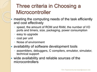
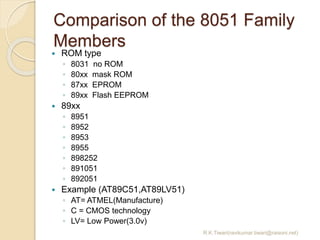
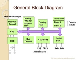
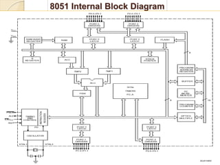
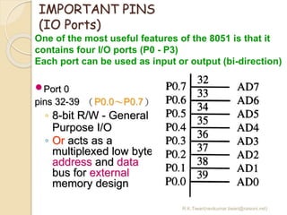
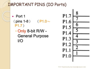
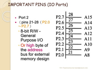
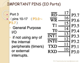
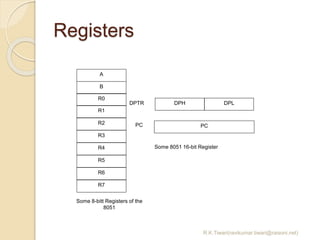
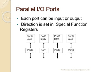
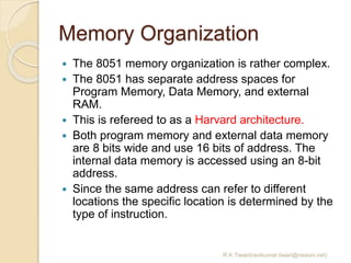
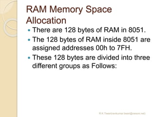
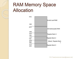
The document discusses the 8051 microcontroller. It provides three key criteria for choosing a microcontroller: 1) meeting computing needs efficiently and cost effectively, 2) availability of software development tools, and 3) reliable sources. It then describes the basic components and features of the 8051, including 4K bytes of ROM, 128 bytes of RAM, four 8-bit I/O ports, two timers/counters, a serial interface, and support for external memory. Finally, it explains the memory organization and allocation of the 8051, distinguishing program memory, data memory, and external RAM.
BASIC INFORMATION OF ARCHITECTURE OF MICRO-CONTROLLER 8051 AS PER GTU SYLLABUS. Please Comment if u Like.. n Give u r feedback..
For More Information Go to
http://www.noesiseducation.blogspot.com
BASIC INFORMATION OF ARCHITECTURE OF MICRO-CONTROLLER 8051 AS PER GTU SYLLABUS. Please Comment if u Like.. n Give u r feedback..
For More Information Go to
http://www.noesiseducation.blogspot.com
Input Output programming in AVR microcontrollerRobo India
Robo India in this presentation presents the Input and Output programming in AVR Micro Controllers namely Atmega 16, Atmega 8, Atmega 328, Atmega 32 etc.
As in robotics, automation and embedded system Input and Output programming is essential. This presentation describes how to use input and output ports, resisters of AVR microcontroller.
If you have any query please write us, we are found at-
website:http://roboindia.com
mail: info@roboindia.com
Complete description of AT89xxx (8051 based) microcontrollers with timers, serial communication and assembly language programming. Interfacing of some real time devices like led, sensor, and seven segment display is also covered.
SYBSC IT SEM IV EMBEDDED SYSTEMS UNIT III The 8051 MicrocontrollersArti Parab Academics
The 8051 Microcontrollers: Microcontrollers and Embedded processors, Overview of 8051 family. 8051 Microcontroller hardware, Input/output pins, Ports, and Circuits, External Memory. 8051 Programming in C: Data Types and time delay in 8051 C, I/O Programming, Logic operations, Data conversion Programs
THIS PDF IS MADE BY OUR TEACHERS OF TEACHERS MS. TRIVENI MAAM ALSO KNOWN AS POLICEPATIL BECAUSE SHES KNOWN TO CHECK POCKETS OF STUDENTS(REGARDLESS OF GENDER) DURING EXAMS. THIS PDF EXPLAINS THE 8051 MICROCONTROLLER.
This presentation discusses the internal architecture of Intel 8051. It discusses basic families of 8051, the programmer view, register sets and memory organiszation of 8051
Course Outcome and Program Outcome Calculation(new method)Ravikumar Tiwari
This presentation explains the new method (based on attainment level) of Course Outcome and Program Outcome Calculation. (with reference to National Board of Accreditation new SAR)
Water scarcity is the lack of fresh water resources to meet the standard water demand. There are two type of water scarcity. One is physical. The other is economic water scarcity.
Hybrid optimization of pumped hydro system and solar- Engr. Abdul-Azeez.pdffxintegritypublishin
Advancements in technology unveil a myriad of electrical and electronic breakthroughs geared towards efficiently harnessing limited resources to meet human energy demands. The optimization of hybrid solar PV panels and pumped hydro energy supply systems plays a pivotal role in utilizing natural resources effectively. This initiative not only benefits humanity but also fosters environmental sustainability. The study investigated the design optimization of these hybrid systems, focusing on understanding solar radiation patterns, identifying geographical influences on solar radiation, formulating a mathematical model for system optimization, and determining the optimal configuration of PV panels and pumped hydro storage. Through a comparative analysis approach and eight weeks of data collection, the study addressed key research questions related to solar radiation patterns and optimal system design. The findings highlighted regions with heightened solar radiation levels, showcasing substantial potential for power generation and emphasizing the system's efficiency. Optimizing system design significantly boosted power generation, promoted renewable energy utilization, and enhanced energy storage capacity. The study underscored the benefits of optimizing hybrid solar PV panels and pumped hydro energy supply systems for sustainable energy usage. Optimizing the design of solar PV panels and pumped hydro energy supply systems as examined across diverse climatic conditions in a developing country, not only enhances power generation but also improves the integration of renewable energy sources and boosts energy storage capacities, particularly beneficial for less economically prosperous regions. Additionally, the study provides valuable insights for advancing energy research in economically viable areas. Recommendations included conducting site-specific assessments, utilizing advanced modeling tools, implementing regular maintenance protocols, and enhancing communication among system components.
Immunizing Image Classifiers Against Localized Adversary Attacksgerogepatton
This paper addresses the vulnerability of deep learning models, particularly convolutional neural networks
(CNN)s, to adversarial attacks and presents a proactive training technique designed to counter them. We
introduce a novel volumization algorithm, which transforms 2D images into 3D volumetric representations.
When combined with 3D convolution and deep curriculum learning optimization (CLO), itsignificantly improves
the immunity of models against localized universal attacks by up to 40%. We evaluate our proposed approach
using contemporary CNN architectures and the modified Canadian Institute for Advanced Research (CIFAR-10
and CIFAR-100) and ImageNet Large Scale Visual Recognition Challenge (ILSVRC12) datasets, showcasing
accuracy improvements over previous techniques. The results indicate that the combination of the volumetric
input and curriculum learning holds significant promise for mitigating adversarial attacks without necessitating
adversary training.
Student information management system project report ii.pdfKamal Acharya
Our project explains about the student management. This project mainly explains the various actions related to student details. This project shows some ease in adding, editing and deleting the student details. It also provides a less time consuming process for viewing, adding, editing and deleting the marks of the students.
2. Three criteria in Choosing a
Microcontroller
R.K.Tiwari(ravikumar.tiwari@raisoni.net)
meeting the computing needs of the task efficiently
and cost effectively
◦ speed, the amount of ROM and RAM, the number of I/O
ports and timers, size, packaging, power consumption
◦ easy to upgrade
◦ cost per unit
◦ Noise of environment
availability of software development tools
◦ assemblers, debuggers, C compilers, emulator, simulator,
technical support
wide availability and reliable sources of the
microcontrollers
3. Comparison of the 8051 Family
Members
R.K.Tiwari(ravikumar.tiwari@raisoni.net)
ROM type
◦ 8031 no ROM
◦ 80xx mask ROM
◦ 87xx EPROM
◦ 89xx Flash EEPROM
89xx
◦ 8951
◦ 8952
◦ 8953
◦ 8955
◦ 898252
◦ 891051
◦ 892051
Example (AT89C51,AT89LV51)
◦ AT= ATMEL(Manufacture)
◦ C = CMOS technology
◦ LV= Low Power(3.0v)
4. 8051 Basic Component/
Feature
R.K.Tiwari(ravikumar.tiwari@raisoni.net)
4K bytes internal ROM
128 bytes internal RAM
Four 8-bit I/O ports (P0 - P3).
Two 16-bit timers/counters
One serial interface
64k external memory for code
64k external memory for data
210 bit addressable
5. The basic 8051 Core
R.K.Tiwari(ravikumar.tiwari@raisoni.net)
• 8-bit CPU optimized for control applications
• Capability for single bit Boolean operations.
• Supports up to 64K of program memory.
• Supports up to 64K of data memory.
• 4 K bytes of on-chip program memory.
• Newer devices provide more.
• 128 or 256 bytes of on-chip data RAM
• Four 8 bit ports.
• Two 16-bit timer/counters
• UART
• Interrupts
• On-chip clock oscillator
12. R.K.Tiwari(ravikumar.tiwari@raisoni.net)
IMPORTANT PINS
(IO Ports)
One of the most useful features of the 8051 is that it
contains four I/O ports (P0 - P3)
Each port can be used as input or output (bi-direction)
Port 0
pins 32-39 (P0.0~P0.7)
◦ 8-bit R/W - General
Purpose I/O
◦ Or acts as a
multiplexed low byte
address and data
bus for external
memory design
17. R.K.Tiwari(ravikumar.tiwari@raisoni.net)
ALE - Address latch enable
to select valid address
EA/Vpp - External access enable
EA-0 execute program in external
memory
EA-1 execute program in internal
memory
Vpp it receives 21 V for on chip EPROM
PSEN Program store enable
store to read the external program memory
19. Parallel I/O Ports
• Each port can be input or output
• Direction is set in Special Function
Registers
R.K.Tiwari(ravikumar.tiwari@raisoni.net)
Port0
latch
Port1
latch
Port2
latch
Port3
latch
Port0 Port1 Port2 Port3
20. DPTR
The data pointer consists of a high
byte(DPH) and a low byte (DPL). Its
function is to hold a 16 bit address. It
may be manipulated as a 16 bit data
register or two independent 8 bit
register. It serves as a base register in
indirect jumps, lookup table
instructions and external data transfer.
R.K.Tiwari(ravikumar.tiwari@raisoni.net)
22. Memory Organization
The 8051 memory organization is rather complex.
The 8051 has separate address spaces for
Program Memory, Data Memory, and external
RAM.
This is refereed to as a Harvard architecture.
Both program memory and external data memory
are 8 bits wide and use 16 bits of address. The
internal data memory is accessed using an 8-bit
address.
Since the same address can refer to different
locations the specific location is determined by the
type of instruction.
R.K.Tiwari(ravikumar.tiwari@raisoni.net)
23. RAM Memory Space
Allocation
There are 128 bytes of RAM in 8051.
The 128 bytes of RAM inside 8051 are
assigned addresses 00h to 7FH.
These 128 bytes are divided into three
different groups as Follows:
R.K.Tiwari(ravikumar.tiwari@raisoni.net)
24. RAM Memory Space
Allocation
1. A total of 32 bytes from location 00
to 1F hex are set aside for register
banks and the stack( 4 register bank
each of 8 byte)
2. A total of 16 byte from location 20h
to 2F h are set aside for bit
addressable RAM.
3. A total of 80bytes from 30h to 7Fh
are used for RD/WR storage which is
normally called as Scratch Pad.
R.K.Tiwari(ravikumar.tiwari@raisoni.net)
26. Stack in the 8051
R.K.Tiwari(ravikumar.tiwari@raisoni.net)
7FH
30H
2FH
20H
1FH
17H
10H
0FH
07H
08H
18H
00H
Register Bank 0
(Stack) Register Bank
1
Register Bank 2
Register Bank 3
Bit-Addressable RAM
Scratch pad RAM
The register used to access
the stack is called SP (stack
pointer) register.
The stack pointer in the
8051 is only 8 bits wide,
which means that it can
take value 00 to FFH. When
8051 powered up, the SP
register contains value 07.