Downloaded 188 times

![b. Operation
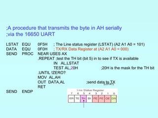
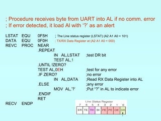
Dialog 16550 Line Status Register (LSTAT)
Programming I/O Address: A2 A1 A0 = 101
Before reading data
from receiver, ensure
RX has data
[DR (bit 1) = 1]
Error status bits
Any being 1 indicates
An error
Before writing data
for transmission,
Ensure TX is ready
to take it
[TH (bit 5) = 1]](https://image.slidesharecdn.com/uart16550-120720150318-phpapp01/85/Uart-16550-15-320.jpg)

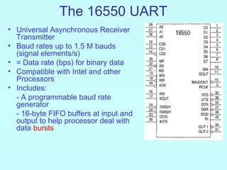
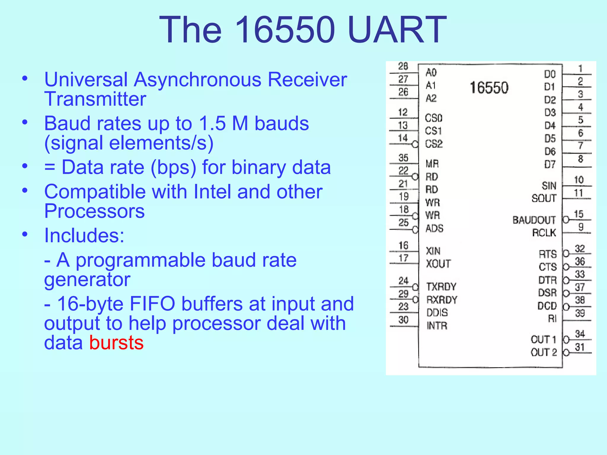
The 16550 UART allows for asynchronous serial communication up to 1.5Mbps. It contains independent transmitter and receiver sections that allow for simplex, half-duplex, and full-duplex communication modes. The UART uses a programmable baud rate generator and 16-byte FIFO buffers to interface with processors. It is commonly used to control serial ports on PCs using two I/O address ranges. Programming involves initializing the line control register and baud rate generator, then performing the actual communication by reading and writing data using the FIFO and line status registers.