Download to read offline

![USART Transmitter program using C-language
Object : Writing firmware to control USART Transmitter
Configuring Internal Registers:
UCSRB|=0x69;
UBRR|=0x67; baud rate 9600 at f=16MHz
UCSRC|=0x26; aysn, evenparity,1-stopbit, data size 8-bit
Flow chart : Tx_data()
Start Start
Enable TX complete Load byte in UDR
interrupt, usart data reg register
empty interrupt, Tx
enable, Txt 8-bits
Byte NO
transmitted
Select baudrate 9600 at 10
?
16MHz, asyn even parity bytes
NO txd ? YE
1-stop ,data bits-8
S
YES
Make TXC bit zero
Call Tx_data(data[i]) End
End](https://image.slidesharecdn.com/presentation-121229020117-phpapp02/85/Presentation-8-320.jpg)

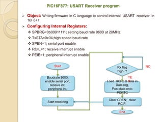
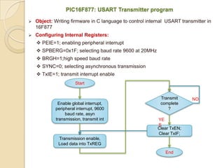


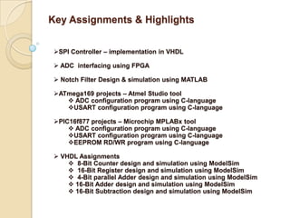
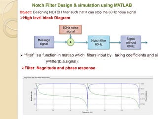
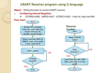
The document describes projects completed as part of an internship program involving digital signal processing and microcontroller programming. Key projects included implementing an SPI controller in VHDL, interfacing an ADC to an FPGA, designing a notch filter in MATLAB, and programming ATmega169 and PIC16F877 microcontrollers to configure ADCs and USART using C language.