
Download as PDF, PPTX

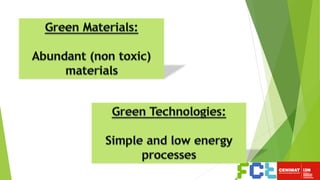


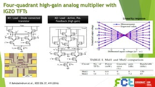
![Freq. response
Circuit No. of
TFTs
C (pF) Power
(mW)
Bandwidth
(kHz)
Gain
(dB)
Load
Amp3 5 40 0.576 20 22 10 MΩ//16 pF
Amp3 5 330 0.576 5 34 10 MΩ//16 pF
[ref] 16 - 0.9 54 18.7 1 MΩ//2 pF
Analog blocks with high-gain topology with IGZO TFTs
P. Bahubalindruni et al., IEEE JDT 11 (2015)
Functional verification, kHz
Adder-subtractor Amplifier](https://image.slidesharecdn.com/sbmat2016fortunatopublicversion-161005222619/85/Green-electronics-a-technology-for-a-sustainable-future-31-320.jpg)


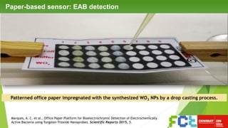

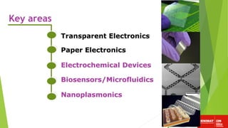
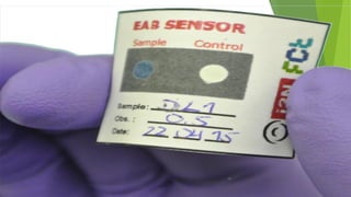
![Colorimetric assays - optimization
10 µL 15 g/L h - WO3 NPs
20 µL Gs and E. coli
Well diameter: 3.38 mm
15 g/L: linear response
EAB detection at latent phase
Response time ~ 2 hours
[Gs]
[WO3NPs]
Marques, A. C. et al., Office Paper Platform for Bioelectrochromic Detection of Electrochemically
Active Bacteria using Tungsten Trioxide Nanoprobes. Scientific Reports 2015, 5.](https://image.slidesharecdn.com/sbmat2016fortunatopublicversion-161005222619/85/Green-electronics-a-technology-for-a-sustainable-future-74-320.jpg)


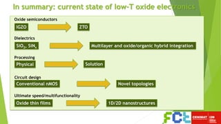
The document discusses advancements in green electronics, specifically focusing on oxide and paper electronics, and their applications in creating sustainable technologies. It highlights key areas such as transparent electronics, flexible devices, and biosensors, while also addressing challenges and opportunities in the field. The findings emphasize the need for enhanced performance and stability in oxide thin-film transistors and explore the benefits of using paper as a substrate for eco-friendly electronic devices.


