
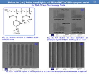
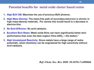
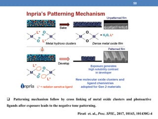
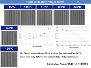
Download as PDF, PPTX
![53
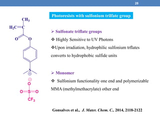
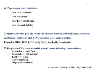
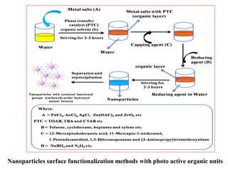
The high EUV harvesting metal oxide nano particles such as HfO2, In2O3, SnO2, Sb2O3, ZrO2,TiO2
and Ag2O etc., capped with photosensitive capping agents : photoactive sulfonium triflates.
During EUV exposure, highly sensitive aromatic sulfonium triflates undergo structural changes
from hydrophilic sulfonium triflates (polar) into hydrophobic aromatic sulfide entities (non-polar)
which leads to the nano patterning.
Nanoscale resists for EUVL (I) [Nano non-CARS]](https://image.slidesharecdn.com/plenariakengonsalves-170923220533/85/Extreme-Ultraviolet-Litography-EUVL-novel-patterning-materials-progress-and-challenges-53-320.jpg)
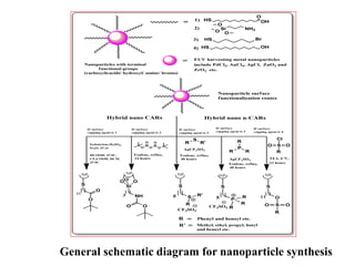
![54
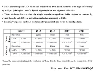
High EUV harvesting nanoparticles modified by introducing two different functional
capping agents: 1) Capping agents with photosensitive sulfonium triflates 2) capping
structures with acid labile functional groups
Nanoscale resists for EUVL (II) [Nano-CARs]](https://image.slidesharecdn.com/plenariakengonsalves-170923220533/85/Extreme-Ultraviolet-Litography-EUVL-novel-patterning-materials-progress-and-challenges-54-320.jpg)

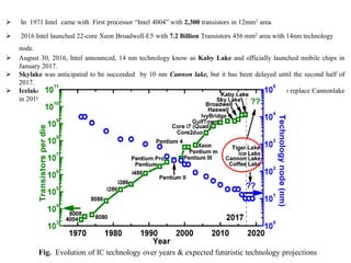
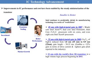
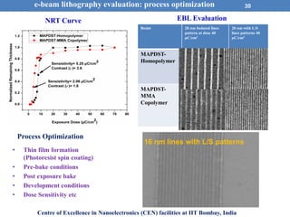
The document discusses progress in extreme ultraviolet lithography (EUVL) for semiconductor fabrication. It covers: 1) EUVL is a promising next-generation lithography technique needed to continue transistor scaling below 7nm, but faces challenges like resolution, line width roughness, and sensitivity. 2) Novel resist materials without chemical amplification are being developed to overcome issues with chemically amplified resists at small scales. Examples discussed are sulfonium-containing polymers that change solubility upon EUV exposure. 3) Experiments show these new resists can resolve lines as small as 16nm and complex nanostructures when exposed with EUV lithography. Continued improvements aim to enhance sensitivity.


![Thin_Film_Technology_introduction[1]](https://cdn.slidesharecdn.com/ss_thumbnails/1b4496c8-2102-411b-8465-a3dd3f398327-150205034538-conversion-gate02-thumbnail.jpg?width=640&height=640&fit=bounds)


