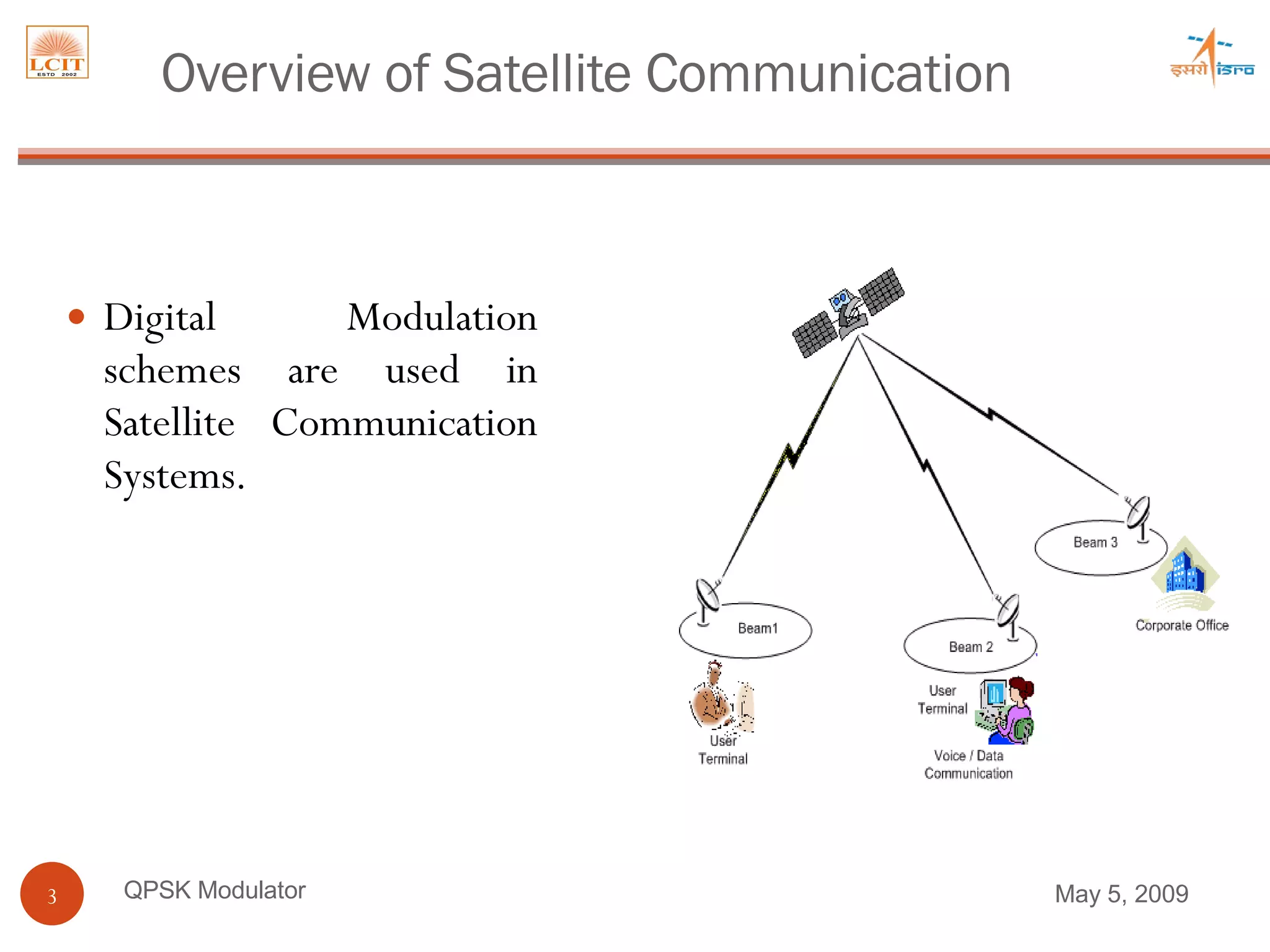
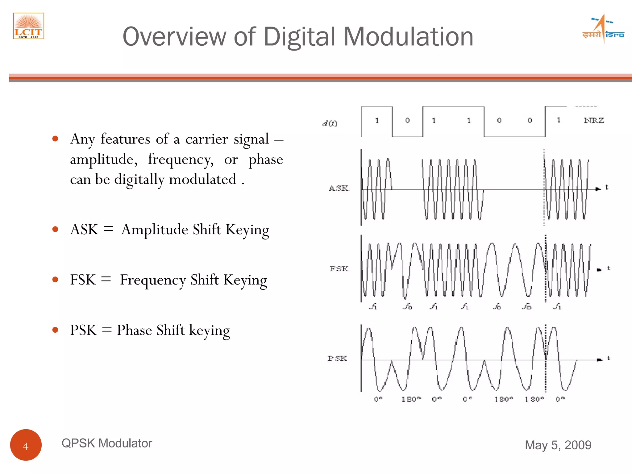
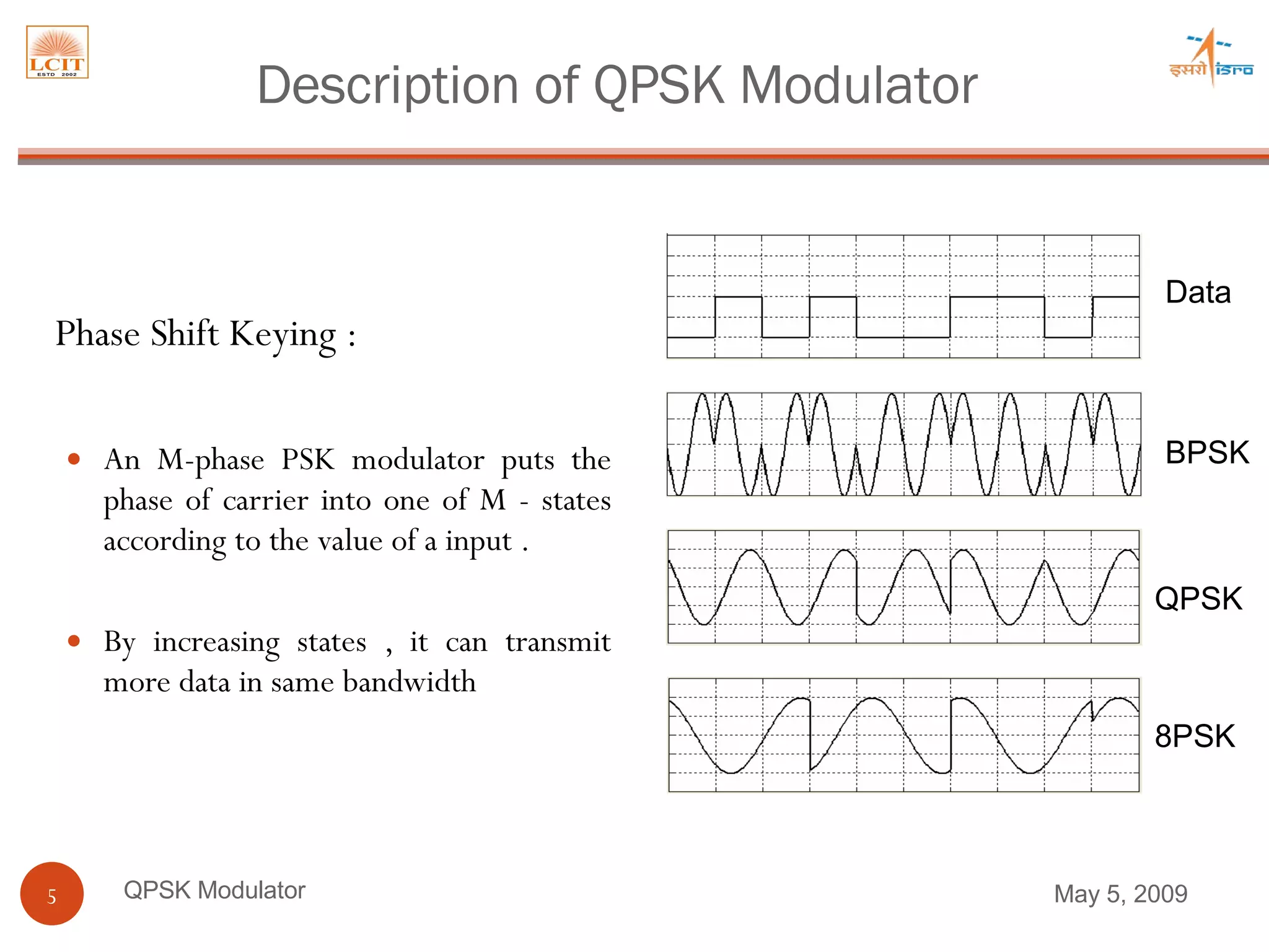
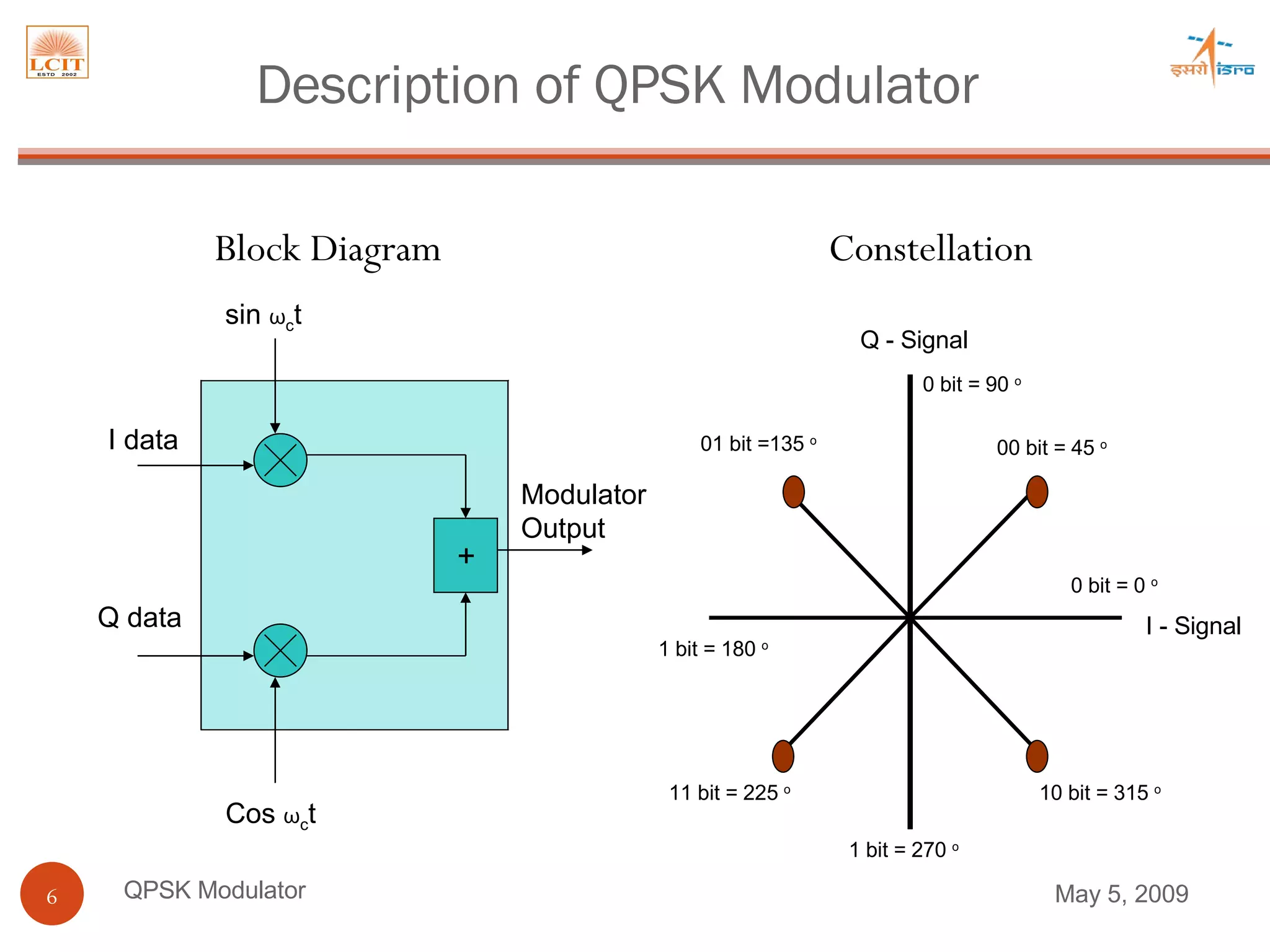
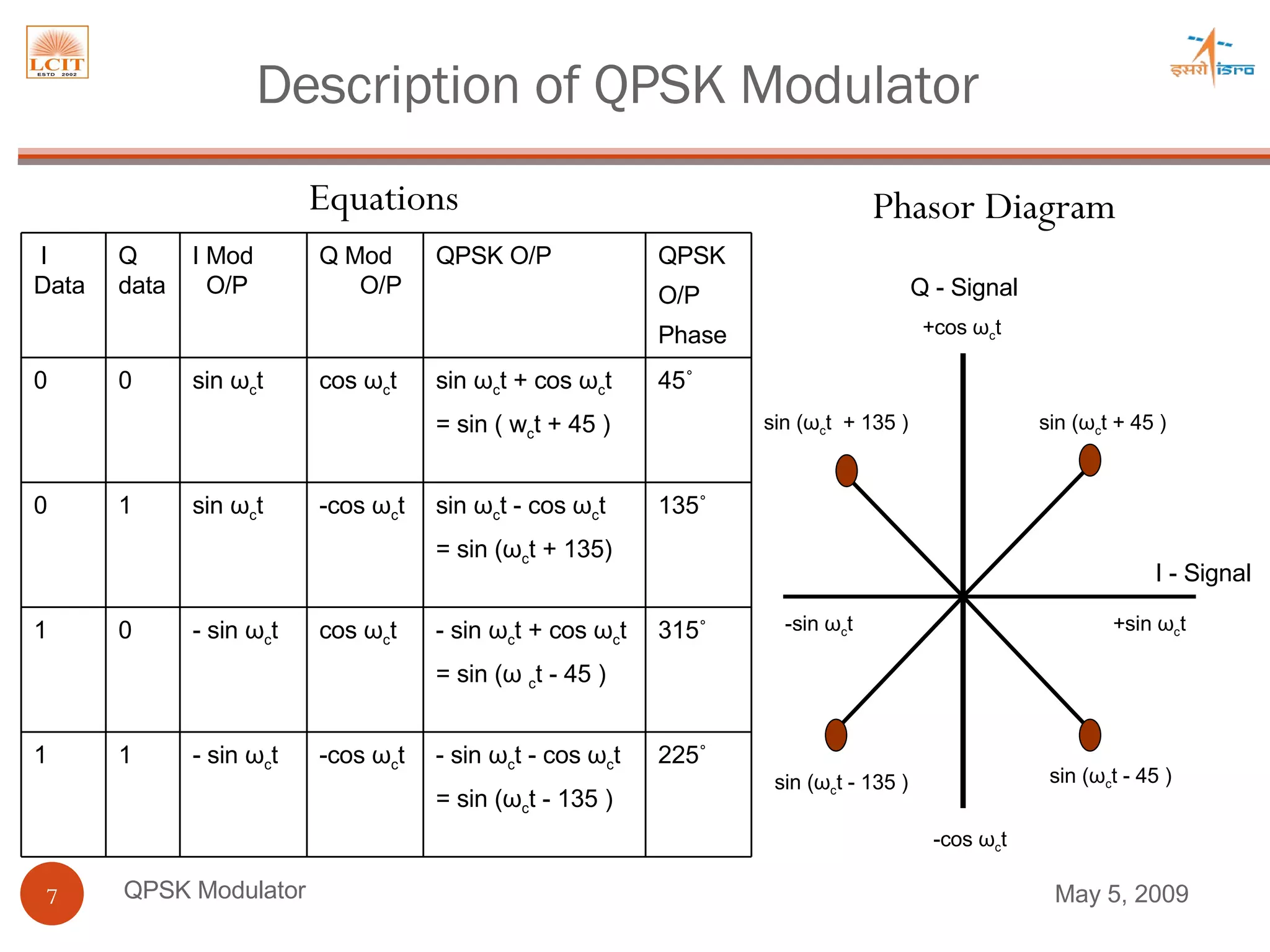
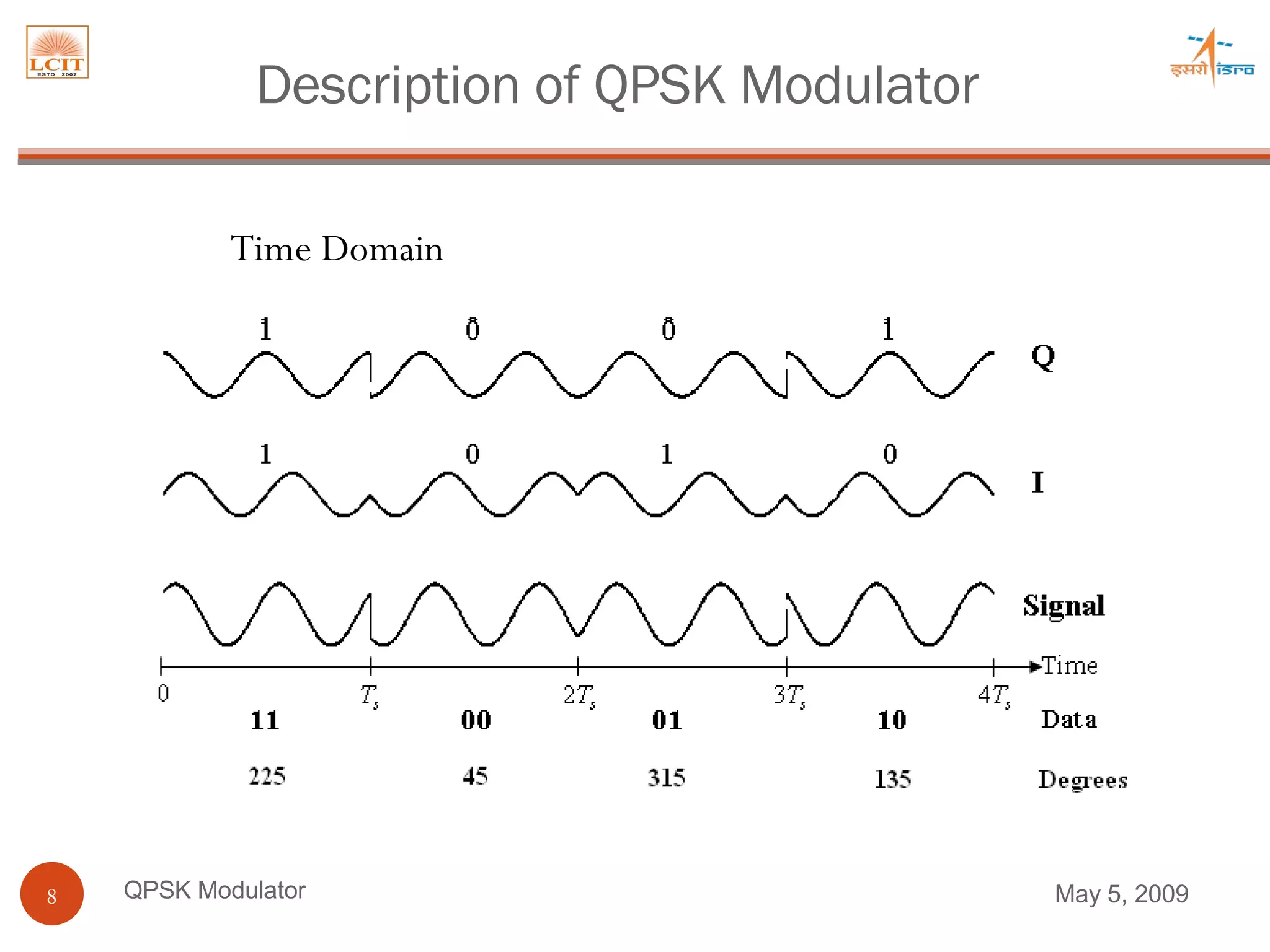
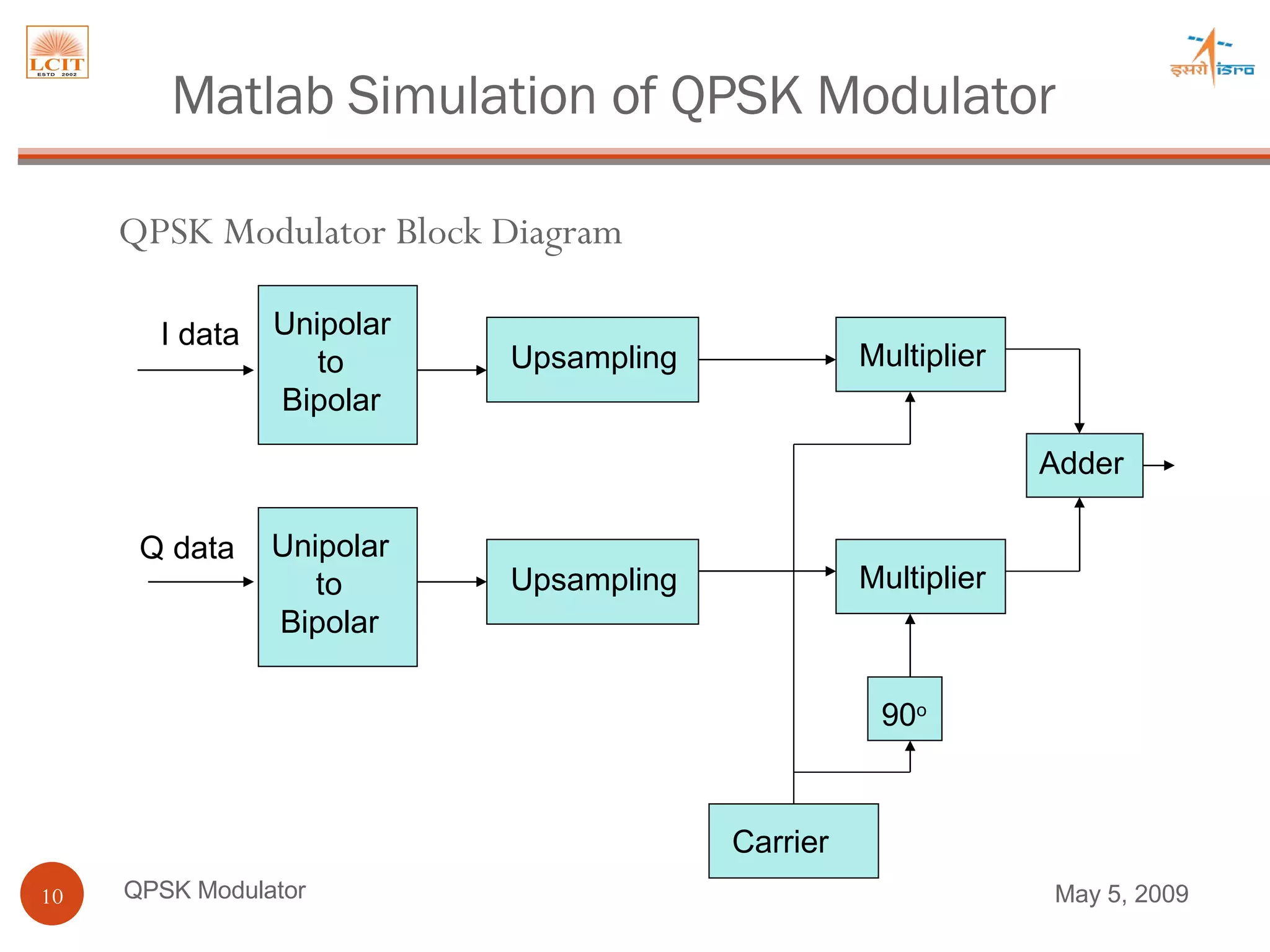
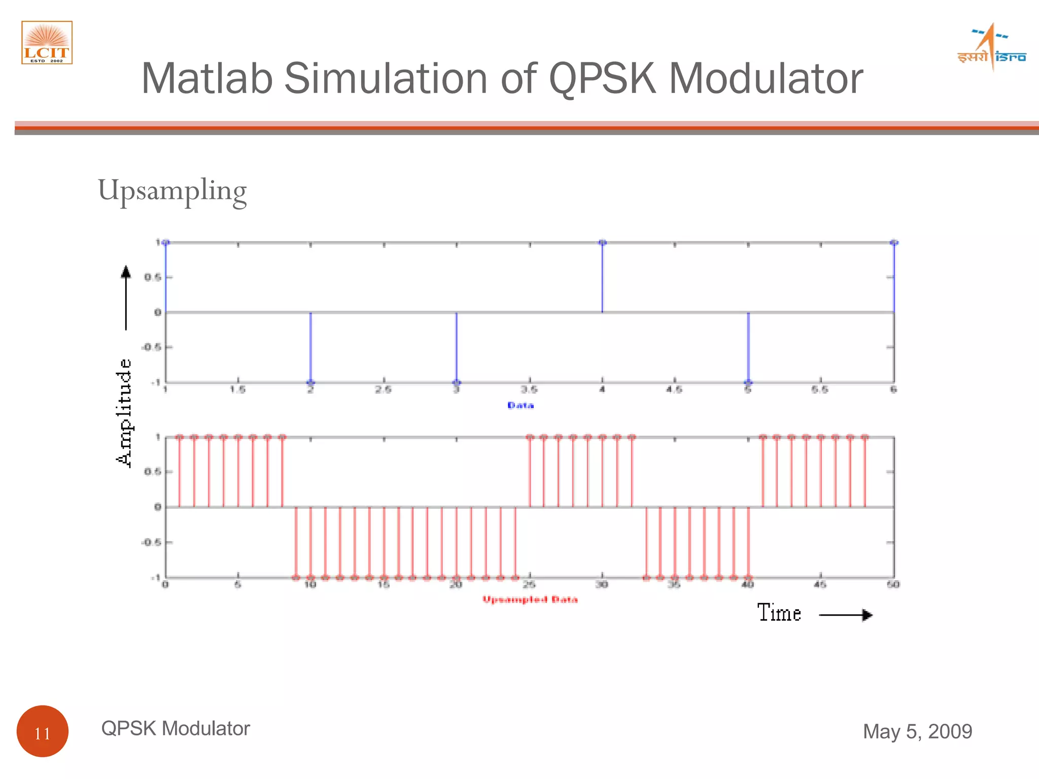
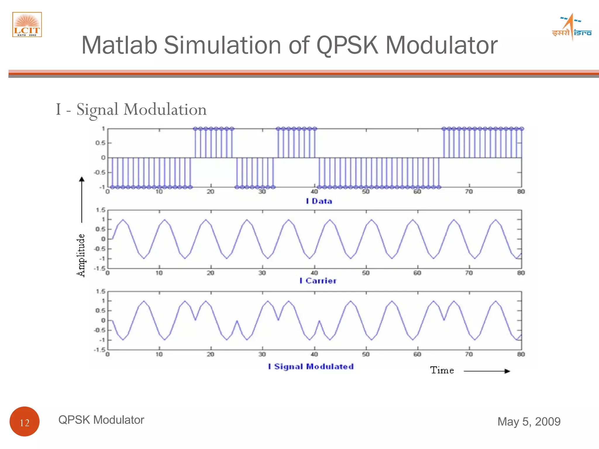
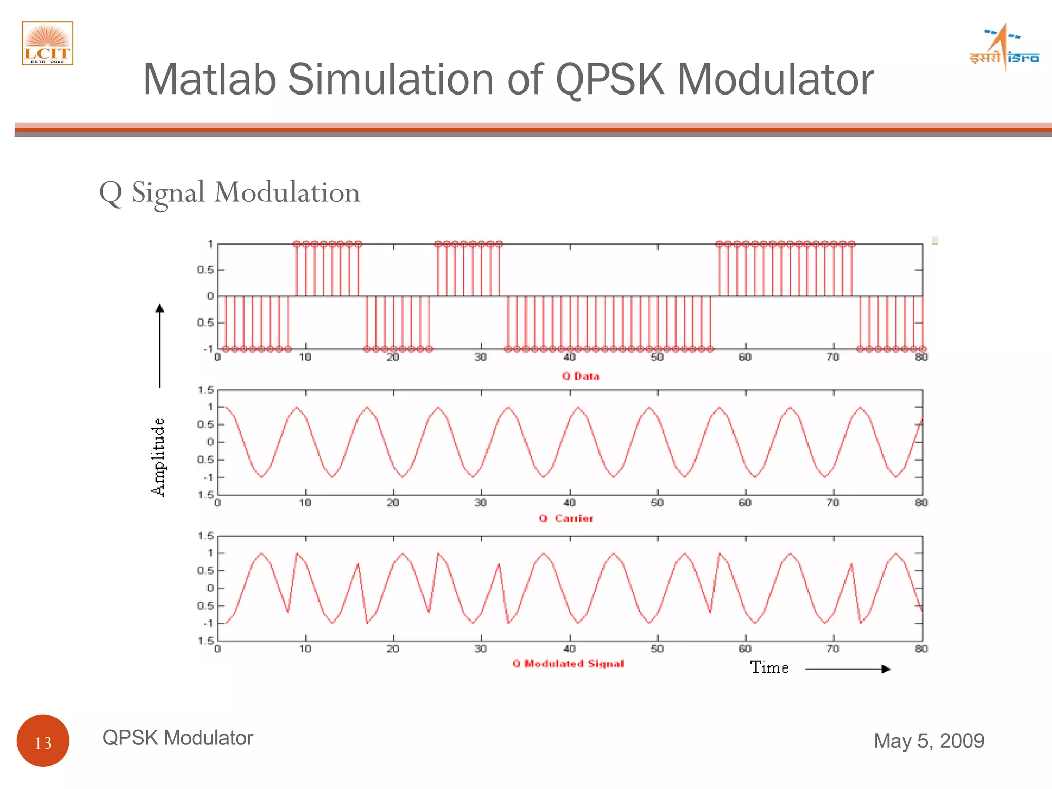
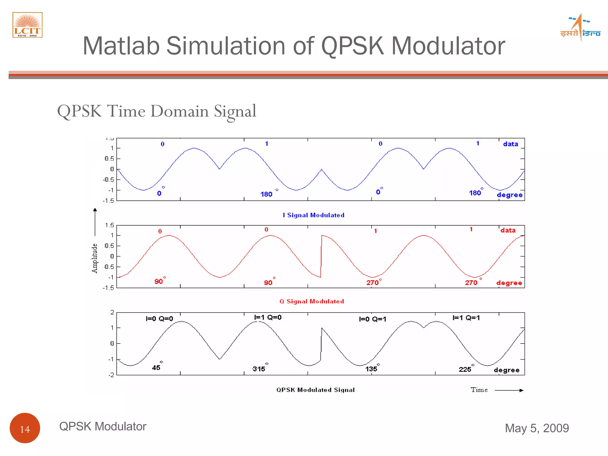
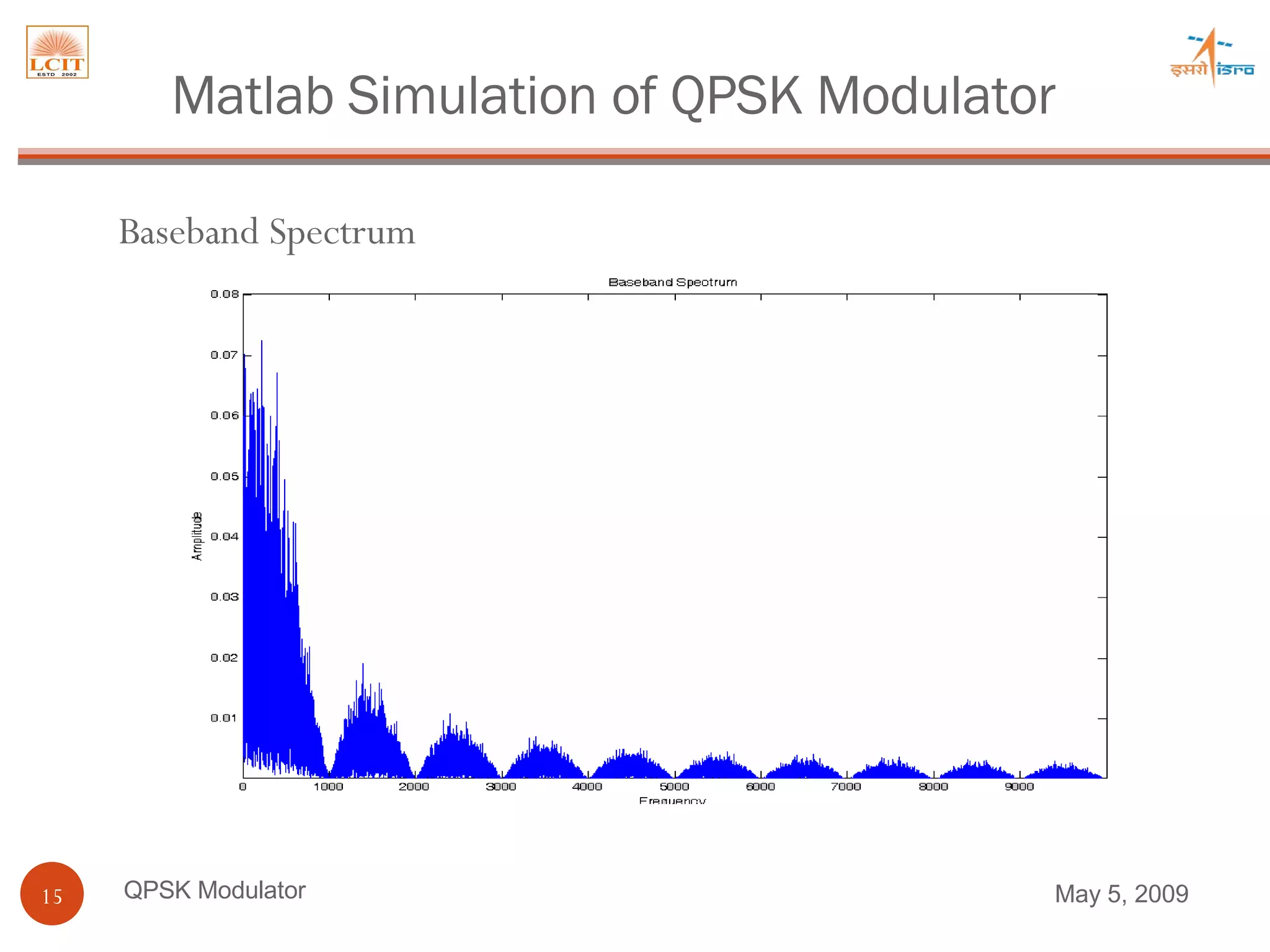
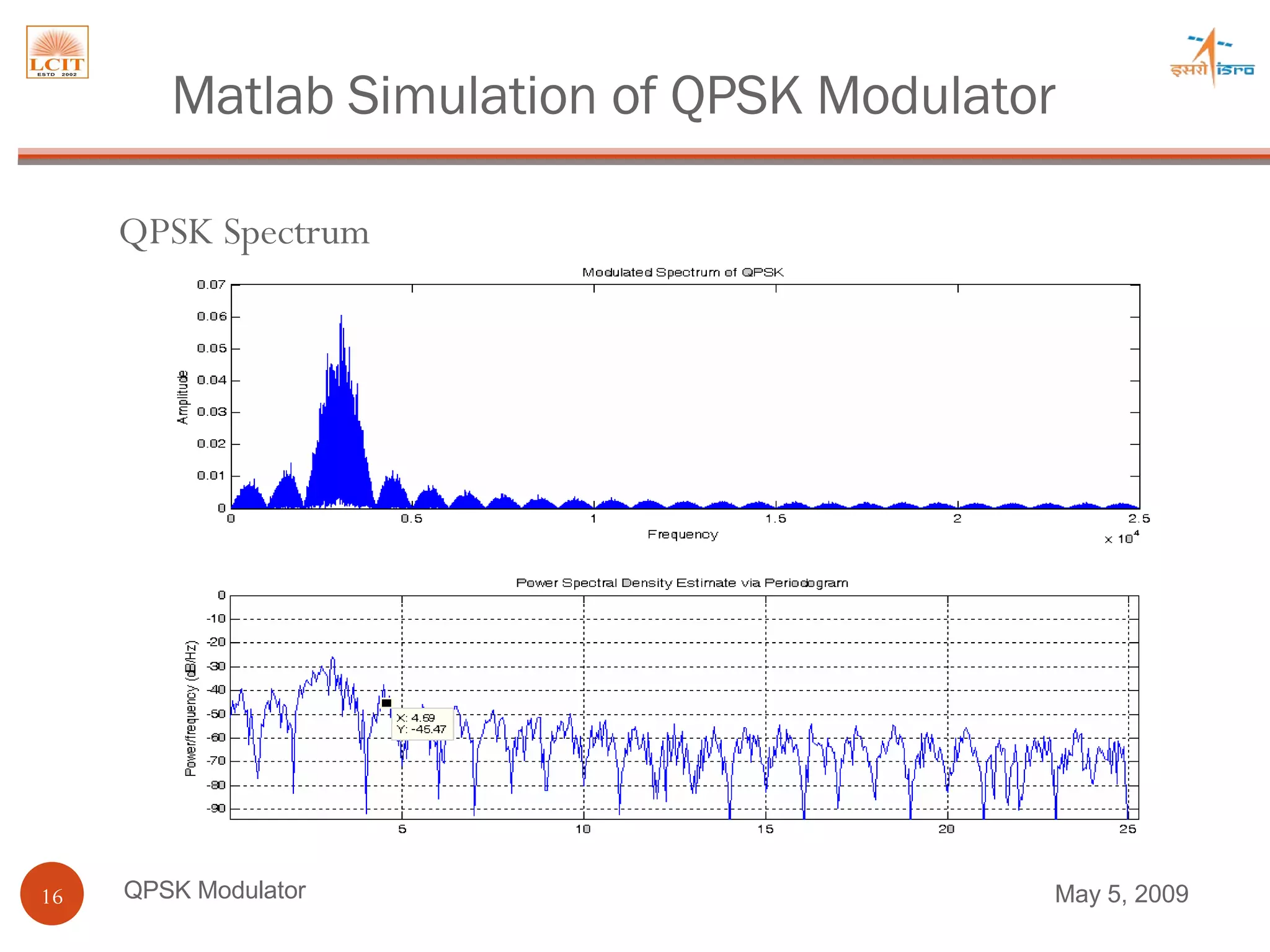
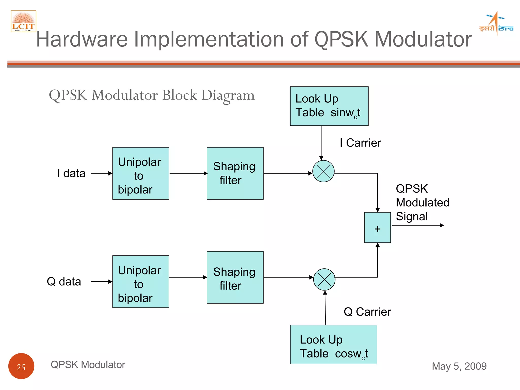
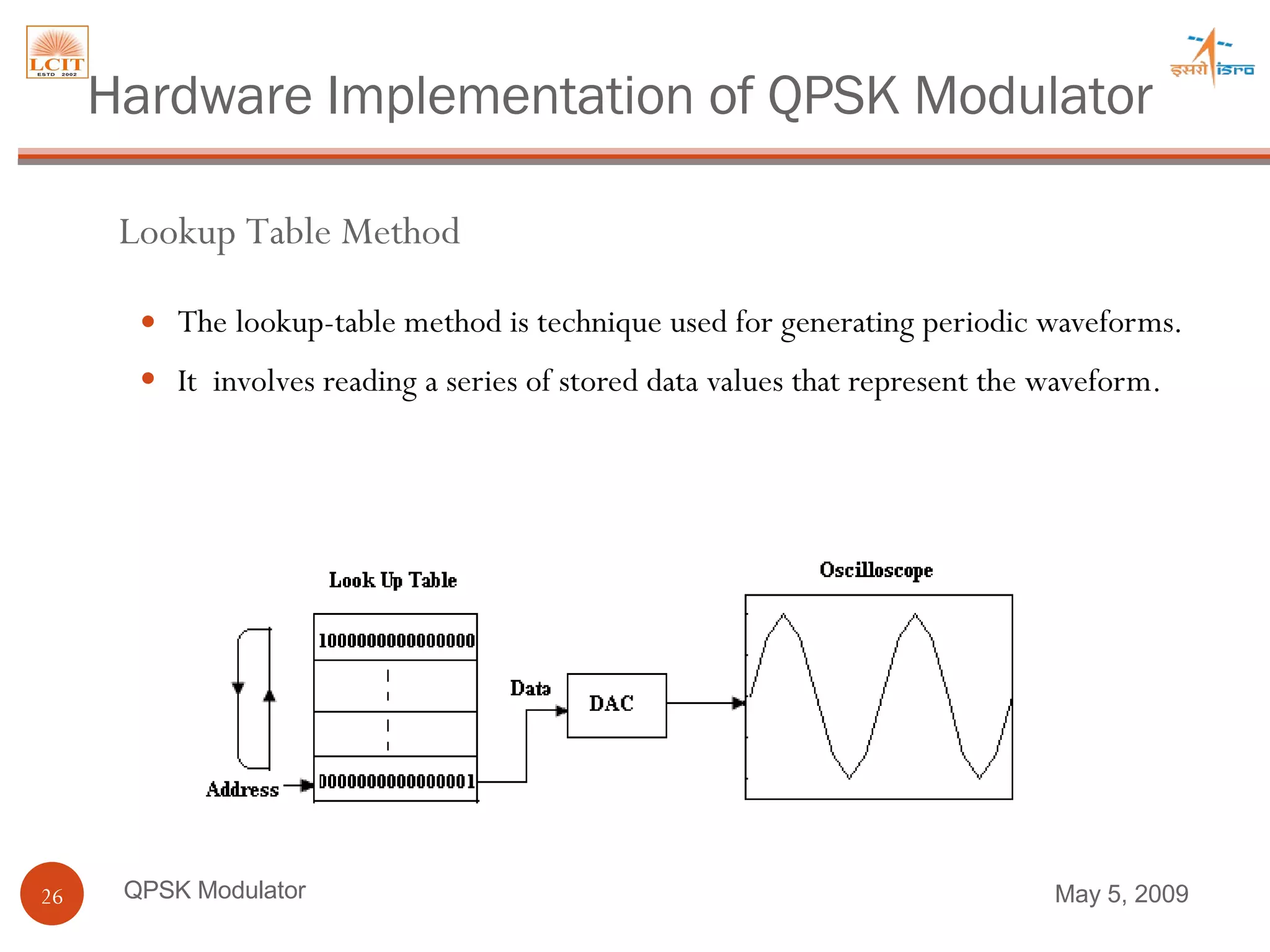
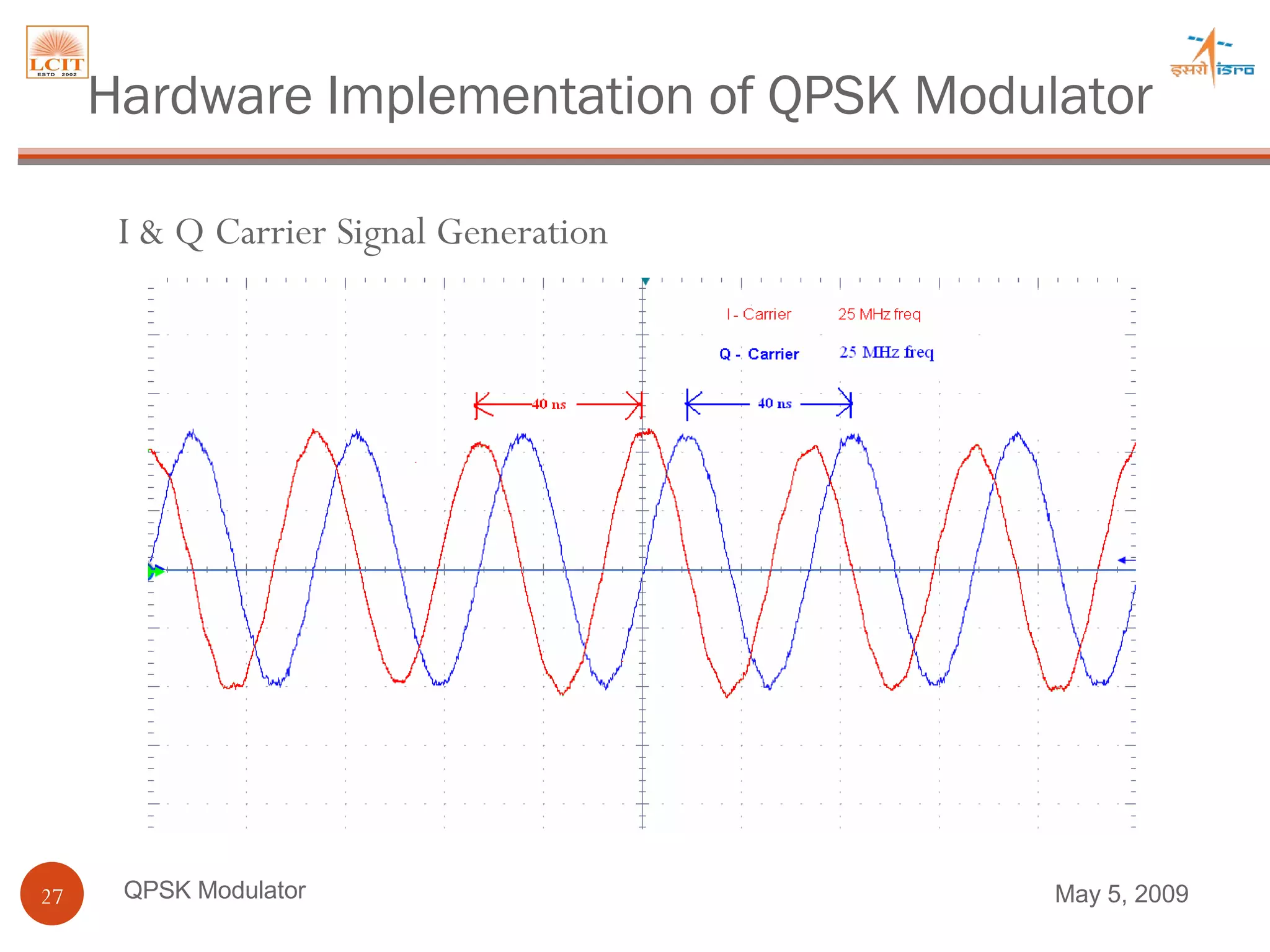
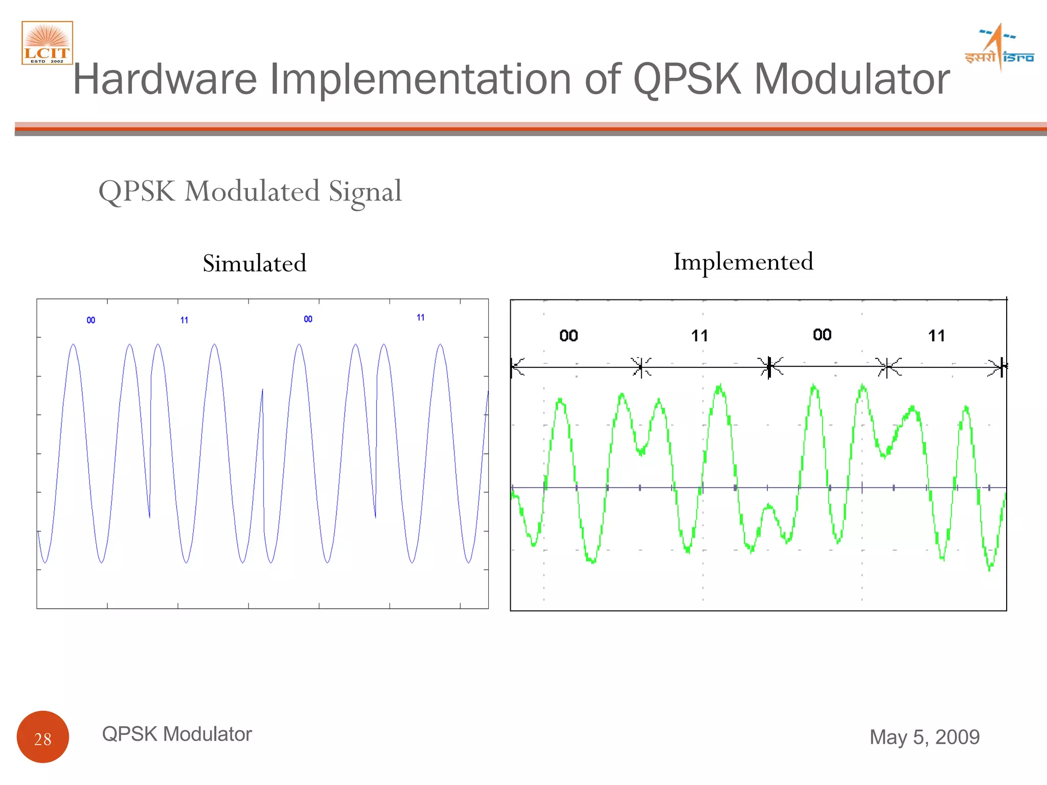
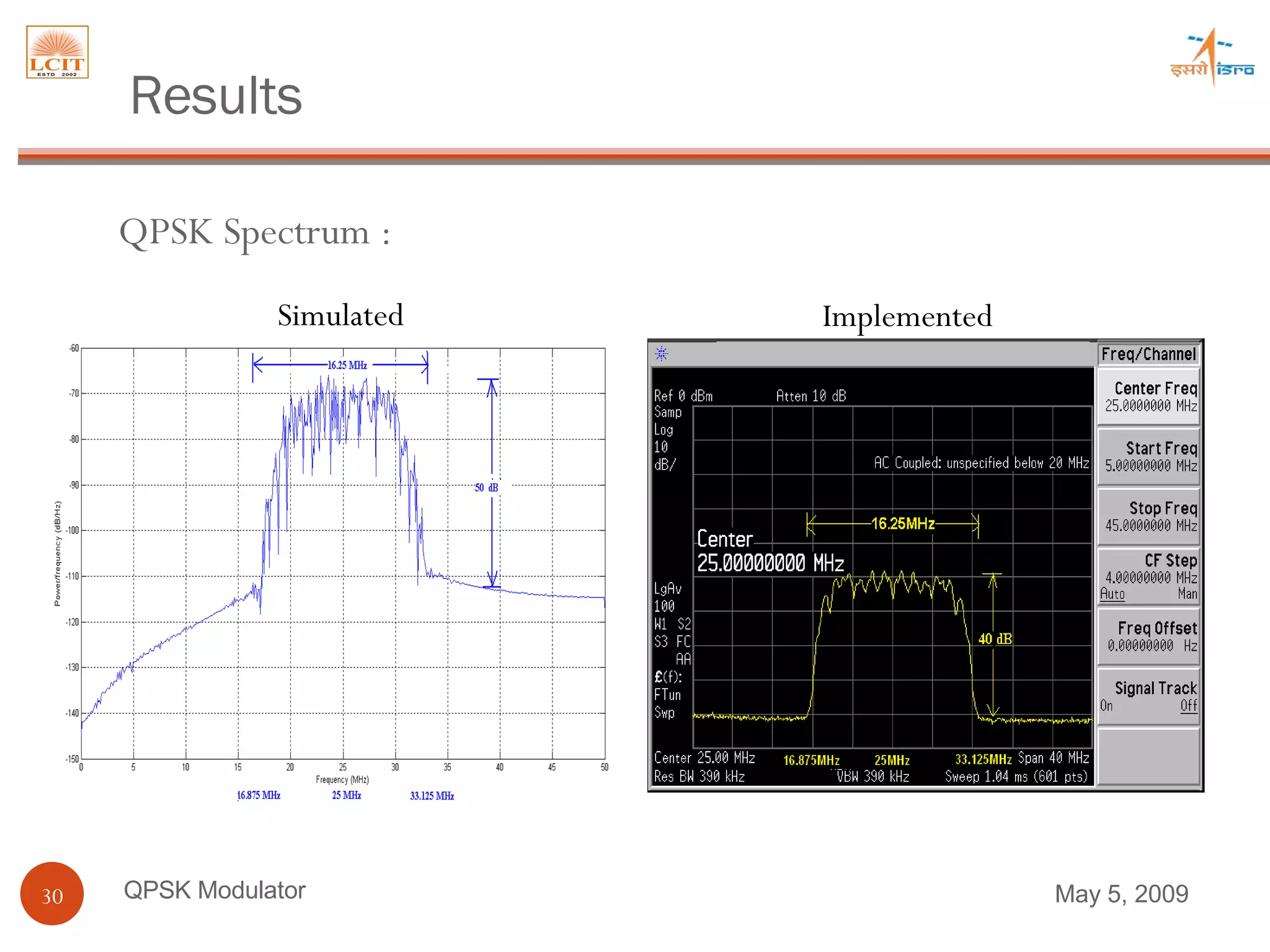
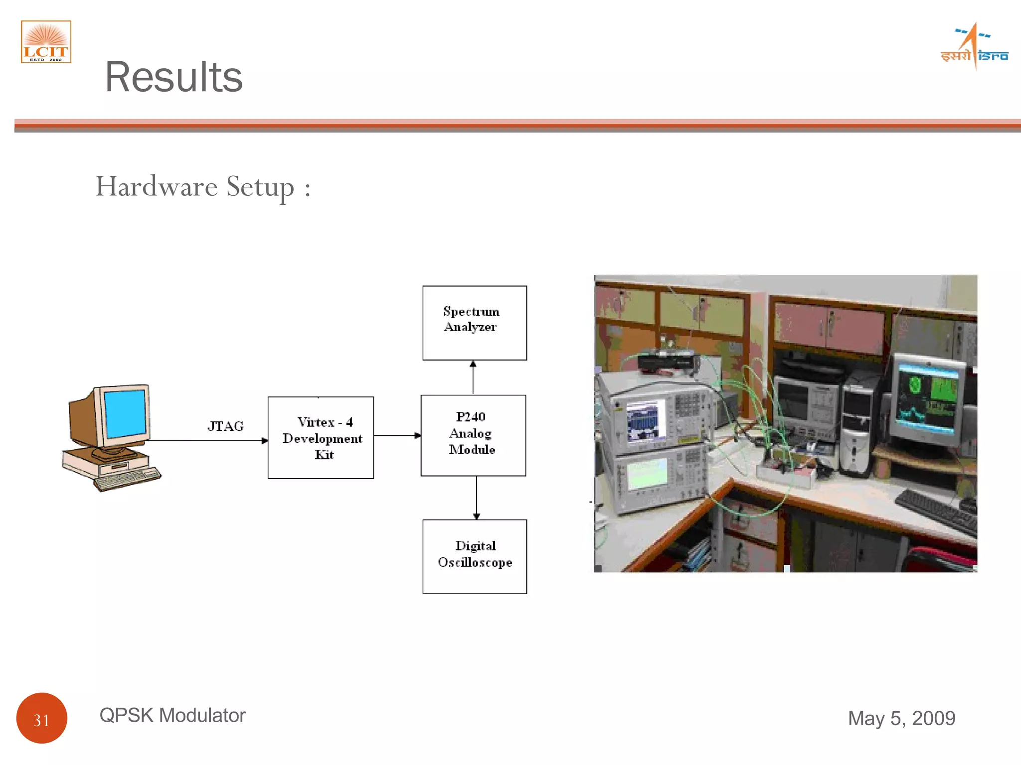
Hardware Implementation of QPSK Modulator for Satellite Communication Presented By : Kiran Prajapati Pradeep Santdasani Internal Guide : Dhara Shah Lecturer (EC Dept.) L C Institute of Tech . External Guide : E P Balasubramanian Group Director SPSG Space Application Center (ISRO)
Agenda  Overview of Satellite Communication Overview of Digital Modulation Description of QPSK Modulator Steps of Project Implementation Matlab Simulation of QPSK Modulator Hardware Implementation of QPSK Modulator Results Conclusion Future Scope QPSK Modulator June 9, 2009
Digital Modulation schemes are used in Satellite Communication Systems. Overview of Satellite Communication QPSK Modulator June 9, 2009
Overview of Digital Modulation Any features of a carrier signal – amplitude, frequency, or phase can be digitally modulated .  ASK =  Amplitude Shift Keying FSK =  Frequency Shift Keying PSK = Phase Shift keying QPSK Modulator June 9, 2009
An M-phase PSK modulator puts the phase of carrier into one of M - states according to the value of a input . By increasing states , it can transmit more data in same bandwidth QPSK Modulator Data BPSK QPSK 8PSK Phase Shift Keying :  Description of QPSK Modulator June 9, 2009
QPSK Modulator I data Q data + Cos  ω c t   Modulator Output Block Diagram sin  ω c t   I - Signal 1 bit = 180  o 0 bit = 0  o  0 bit = 90  o 00 bit = 45  o 10 bit = 315  o 01 bit =135  o 11 bit = 225  o Q - Signal 1 bit = 270  o Constellation Description of QPSK Modulator June 9, 2009
QPSK Modulator Equations I - Signal sin ( ω c t - 45 ) Q - Signal -cos  ω c t Phasor Diagram +cos  ω c t +sin  ω c t -sin  ω c t sin ( ω c t - 135 ) sin ( ω c t + 45 ) sin ( ω c t  + 135 ) Description of QPSK Modulator June 9, 2009 I  Data Q data I Mod  O/P  Q Mod  O/P  QPSK O/P QPSK  O/P Phase 0 0 sin  ω c t cos  ω c t sin  ω c t + cos  ω c t  = sin ( w c t + 45 ) 45˚ 0 1 sin  ω c t -cos  ω c t sin  ω c t - cos  ω c t = sin ( ω c t + 135)  135˚ 1 0 - sin  ω c t cos  ω c t - sin  ω c t + cos  ω c t = sin ( ω   c t - 45 ) 315˚ 1 1 - sin  ω c t -cos  ω c t - sin  ω c t - cos  ω c t = sin ( ω c t - 135 ) 225˚
QPSK Modulator Time Domain Description of QPSK Modulator June 9, 2009
Steps of Project Implementation Matlab Simulation Simulation on Xilinx FPGA Implementation on Virtex – 4 Testing and Debugging QPSK Modulator June 9, 2009
QPSK Modulator Unipolar  to  Bipolar Upsampling Carrier Unipolar  to  Bipolar Upsampling 90 o I data Q data Multiplier Multiplier Adder QPSK Modulator Block Diagram Matlab Simulation of QPSK Modulator June 9, 2009
QPSK Modulator Upsampling Matlab Simulation of QPSK Modulator June 9, 2009
QPSK Modulator I - Signal Modulation Matlab Simulation of QPSK Modulator June 9, 2009
QPSK Modulator Q Signal Modulation Matlab Simulation of QPSK Modulator June 9, 2009
QPSK Modulator QPSK Time Domain Signal Matlab Simulation of QPSK Modulator June 9, 2009
QPSK Modulator Baseband Spectrum Matlab Simulation of QPSK Modulator June 9, 2009
QPSK Modulator QPSK Spectrum Matlab Simulation of QPSK Modulator June 9, 2009
It is used for band limit the signal bandwidth . The  objective is to create a pulse that resembles the sin x/x shape. So that receiver samples at intervals of Tb , where Tb is the bit period . At the sampling instant , the “tails”  from all preceding pulses have  zero values QPSK Modulator Root Cosine Filter Matlab Simulation of QPSK Modulator June 9, 2009
QPSK Modulator Unipolar  to  Bipolar Upsampling Carrier Unipolar  to  Bipolar Upsampling 90 o I data Q data Shaping Shaping Multiplier Multiplier Adder QPSK Modulator Block Diagram Matlab Simulation of QPSK Modulator June 9, 2009
QPSK Modulator QPSK Spectrum Matlab Simulation of QPSK Modulator June 9, 2009
QPSK Modulator Carrier Frequency  ƒc = 25 MHz Data Frequency  ƒd = 25 MHz Roll off Factor  α   =  0.3   Bandwidth = 16.25 MHz Matlab Simulation of QPSK Modulator QPSK Bandwidth June 9, 2009
DSP algorithm has sum of products of equations DSP systems are required to perform intensive arithmetic operations such as multiplications and additions.  FPGAs can be used to implement DSP system as they provide tremendous computational power by using highly parallel architecture for high performance.  FPGAs dedicated for DSP has Embedded multipliers and distributed RAM for storage of coefficients. QPSK Modulator Digital Signal Processing (DSP) in FPGA :  Hardware Implementation of QPSK Modulator June 9, 2009
It consists of I/O buffers, an array of configuration logic blocks and programmable interconnect structures.  Programming of the interconnect  structure is accomplished by RAM cells whose o/p terminals are connected to the gates of MOS pass transistor  QPSK Modulator Field Programmable Gate Array (FPGA) Hardware Implementation of QPSK Modulator June 9, 2009
Virtex 4 development kit is based on the  4VSX35 FPGA SX family is focused for DSP  applications  It has embedded multipliers which increases speed in MAC operations QPSK Modulator Virtex – 4 (SX Family) Hardware Implementation of QPSK Modulator June 9, 2009
The Integrated Software Environment (ISE) is the Xilinx design software suite that allows taking design from design entry through Xilinx device programming.   QPSK Modulator Design  Entry Synthesis Implementation Verification Device  Configuration Xilinx ISE Hardware Implementation of QPSK Modulator June 9, 2009
QPSK Modulator I data + Look Up Table  sinw c t  I Carrier Q Carrier Shaping filter Unipolar to  bipolar Shaping filter Unipolar to  bipolar Q data QPSK Modulated Signal Look Up Table  cosw c t  QPSK Modulator Block Diagram Hardware Implementation of QPSK Modulator June 9, 2009
The lookup-table method is technique used for generating periodic waveforms.  It  involves reading a series of stored data values that represent the waveform.   QPSK Modulator Lookup Table Method Hardware Implementation of QPSK Modulator June 9, 2009
QPSK Modulator I & Q Carrier Signal Generation Hardware Implementation of QPSK Modulator June 9, 2009
QPSK Modulator Simulated Implemented QPSK Modulated Signal Hardware Implementation of QPSK Modulator June 9, 2009
QPSK Modulator QPSK Spectrum Hardware Implementation of QPSK Modulator June 9, 2009
QPSK Modulator Simulated Implemented QPSK Spectrum : Results June 9, 2009
QPSK Modulator Hardware Setup : Results June 9, 2009
Conclusion QPSK modulator has been successfully implemented on the Xilinx Virtex – 4 Development kit. QPSK Modulator is simulated in Matlab Software to verify and compare its functionality taking into account the limitations imposed by the hardware  The modulator algorithm has been implemented on FPGA using the VHSIC hardware description language (VHDL) on Xilinx ISE 8.2i. Simulated waveform is compared with actual output on the digital oscilloscope and spectrum analyzer.  The designed modulator may be used as a test bed for the functional verification of various RF subsystems which requires to be parameterized under modulated signal conditions  QPSK Modulator June 9, 2009
QPSK Demodulator Multi Carrier QPSK Modulator  Higher Order Digital Modulator and Demodulator QPSK Modulator The hardware module can be functionally extended to the following to support a variety of applications:  Future Scope June 9, 2009
Modern Digital and Analog Communication Systems By B.P. LATHI Satellite Communication  By William Pratt Contemporary Communication Systems using Matlab By John G. Proakis VHDL Primer By J.Bhasker Digital Systems Design with VHDL and Synthesis By K.C.Chang User Guide of Xilinx ISE Datasheet of Virtex - 4  Datasheet of P240 Prototype Module  QPSK Modulator References June 9, 2009
Thanks

Hardware Implementation Of QPSK Modulator for Satellite Communications

  • 1.
    Hardware Implementation ofQPSK Modulator for Satellite Communication Presented By : Kiran Prajapati Pradeep Santdasani Internal Guide : Dhara Shah Lecturer (EC Dept.) L C Institute of Tech . External Guide : E P Balasubramanian Group Director SPSG Space Application Center (ISRO)
  • 2.
    Agenda Overviewof Satellite Communication Overview of Digital Modulation Description of QPSK Modulator Steps of Project Implementation Matlab Simulation of QPSK Modulator Hardware Implementation of QPSK Modulator Results Conclusion Future Scope QPSK Modulator June 9, 2009
  • 3.
    Digital Modulation schemesare used in Satellite Communication Systems. Overview of Satellite Communication QPSK Modulator June 9, 2009
  • 4.
    Overview of DigitalModulation Any features of a carrier signal – amplitude, frequency, or phase can be digitally modulated . ASK = Amplitude Shift Keying FSK = Frequency Shift Keying PSK = Phase Shift keying QPSK Modulator June 9, 2009
  • 5.
    An M-phase PSKmodulator puts the phase of carrier into one of M - states according to the value of a input . By increasing states , it can transmit more data in same bandwidth QPSK Modulator Data BPSK QPSK 8PSK Phase Shift Keying : Description of QPSK Modulator June 9, 2009
  • 6.
    QPSK Modulator Idata Q data + Cos ω c t Modulator Output Block Diagram sin ω c t I - Signal 1 bit = 180 o 0 bit = 0 o 0 bit = 90 o 00 bit = 45 o 10 bit = 315 o 01 bit =135 o 11 bit = 225 o Q - Signal 1 bit = 270 o Constellation Description of QPSK Modulator June 9, 2009
  • 7.
    QPSK Modulator EquationsI - Signal sin ( ω c t - 45 ) Q - Signal -cos ω c t Phasor Diagram +cos ω c t +sin ω c t -sin ω c t sin ( ω c t - 135 ) sin ( ω c t + 45 ) sin ( ω c t + 135 ) Description of QPSK Modulator June 9, 2009 I Data Q data I Mod O/P Q Mod O/P QPSK O/P QPSK O/P Phase 0 0 sin ω c t cos ω c t sin ω c t + cos ω c t = sin ( w c t + 45 ) 45˚ 0 1 sin ω c t -cos ω c t sin ω c t - cos ω c t = sin ( ω c t + 135) 135˚ 1 0 - sin ω c t cos ω c t - sin ω c t + cos ω c t = sin ( ω c t - 45 ) 315˚ 1 1 - sin ω c t -cos ω c t - sin ω c t - cos ω c t = sin ( ω c t - 135 ) 225˚
  • 8.
    QPSK Modulator TimeDomain Description of QPSK Modulator June 9, 2009
  • 9.
    Steps of ProjectImplementation Matlab Simulation Simulation on Xilinx FPGA Implementation on Virtex – 4 Testing and Debugging QPSK Modulator June 9, 2009
  • 10.
    QPSK Modulator Unipolar to Bipolar Upsampling Carrier Unipolar to Bipolar Upsampling 90 o I data Q data Multiplier Multiplier Adder QPSK Modulator Block Diagram Matlab Simulation of QPSK Modulator June 9, 2009
  • 11.
    QPSK Modulator UpsamplingMatlab Simulation of QPSK Modulator June 9, 2009
  • 12.
    QPSK Modulator I- Signal Modulation Matlab Simulation of QPSK Modulator June 9, 2009
  • 13.
    QPSK Modulator QSignal Modulation Matlab Simulation of QPSK Modulator June 9, 2009
  • 14.
    QPSK Modulator QPSKTime Domain Signal Matlab Simulation of QPSK Modulator June 9, 2009
  • 15.
    QPSK Modulator BasebandSpectrum Matlab Simulation of QPSK Modulator June 9, 2009
  • 16.
    QPSK Modulator QPSKSpectrum Matlab Simulation of QPSK Modulator June 9, 2009
  • 17.
    It is usedfor band limit the signal bandwidth . The objective is to create a pulse that resembles the sin x/x shape. So that receiver samples at intervals of Tb , where Tb is the bit period . At the sampling instant , the “tails” from all preceding pulses have zero values QPSK Modulator Root Cosine Filter Matlab Simulation of QPSK Modulator June 9, 2009
  • 18.
    QPSK Modulator Unipolar to Bipolar Upsampling Carrier Unipolar to Bipolar Upsampling 90 o I data Q data Shaping Shaping Multiplier Multiplier Adder QPSK Modulator Block Diagram Matlab Simulation of QPSK Modulator June 9, 2009
  • 19.
    QPSK Modulator QPSKSpectrum Matlab Simulation of QPSK Modulator June 9, 2009
  • 20.
    QPSK Modulator CarrierFrequency ƒc = 25 MHz Data Frequency ƒd = 25 MHz Roll off Factor α = 0.3 Bandwidth = 16.25 MHz Matlab Simulation of QPSK Modulator QPSK Bandwidth June 9, 2009
  • 21.
    DSP algorithm hassum of products of equations DSP systems are required to perform intensive arithmetic operations such as multiplications and additions. FPGAs can be used to implement DSP system as they provide tremendous computational power by using highly parallel architecture for high performance. FPGAs dedicated for DSP has Embedded multipliers and distributed RAM for storage of coefficients. QPSK Modulator Digital Signal Processing (DSP) in FPGA : Hardware Implementation of QPSK Modulator June 9, 2009
  • 22.
    It consists ofI/O buffers, an array of configuration logic blocks and programmable interconnect structures. Programming of the interconnect structure is accomplished by RAM cells whose o/p terminals are connected to the gates of MOS pass transistor QPSK Modulator Field Programmable Gate Array (FPGA) Hardware Implementation of QPSK Modulator June 9, 2009
  • 23.
    Virtex 4 developmentkit is based on the 4VSX35 FPGA SX family is focused for DSP applications It has embedded multipliers which increases speed in MAC operations QPSK Modulator Virtex – 4 (SX Family) Hardware Implementation of QPSK Modulator June 9, 2009
  • 24.
    The Integrated SoftwareEnvironment (ISE) is the Xilinx design software suite that allows taking design from design entry through Xilinx device programming. QPSK Modulator Design Entry Synthesis Implementation Verification Device Configuration Xilinx ISE Hardware Implementation of QPSK Modulator June 9, 2009
  • 25.
    QPSK Modulator Idata + Look Up Table sinw c t I Carrier Q Carrier Shaping filter Unipolar to bipolar Shaping filter Unipolar to bipolar Q data QPSK Modulated Signal Look Up Table cosw c t QPSK Modulator Block Diagram Hardware Implementation of QPSK Modulator June 9, 2009
  • 26.
    The lookup-table methodis technique used for generating periodic waveforms. It involves reading a series of stored data values that represent the waveform. QPSK Modulator Lookup Table Method Hardware Implementation of QPSK Modulator June 9, 2009
  • 27.
    QPSK Modulator I& Q Carrier Signal Generation Hardware Implementation of QPSK Modulator June 9, 2009
  • 28.
    QPSK Modulator SimulatedImplemented QPSK Modulated Signal Hardware Implementation of QPSK Modulator June 9, 2009
  • 29.
    QPSK Modulator QPSKSpectrum Hardware Implementation of QPSK Modulator June 9, 2009
  • 30.
    QPSK Modulator SimulatedImplemented QPSK Spectrum : Results June 9, 2009
  • 31.
    QPSK Modulator HardwareSetup : Results June 9, 2009
  • 32.
    Conclusion QPSK modulatorhas been successfully implemented on the Xilinx Virtex – 4 Development kit. QPSK Modulator is simulated in Matlab Software to verify and compare its functionality taking into account the limitations imposed by the hardware The modulator algorithm has been implemented on FPGA using the VHSIC hardware description language (VHDL) on Xilinx ISE 8.2i. Simulated waveform is compared with actual output on the digital oscilloscope and spectrum analyzer. The designed modulator may be used as a test bed for the functional verification of various RF subsystems which requires to be parameterized under modulated signal conditions QPSK Modulator June 9, 2009
  • 33.
    QPSK Demodulator MultiCarrier QPSK Modulator Higher Order Digital Modulator and Demodulator QPSK Modulator The hardware module can be functionally extended to the following to support a variety of applications: Future Scope June 9, 2009
  • 34.
    Modern Digital andAnalog Communication Systems By B.P. LATHI Satellite Communication By William Pratt Contemporary Communication Systems using Matlab By John G. Proakis VHDL Primer By J.Bhasker Digital Systems Design with VHDL and Synthesis By K.C.Chang User Guide of Xilinx ISE Datasheet of Virtex - 4 Datasheet of P240 Prototype Module QPSK Modulator References June 9, 2009
  • 35.

Editor's Notes

  • #2 We are doing project in space application centre(isro) at ahmedabad. Our project is QPSK modulator QPSK Modulator