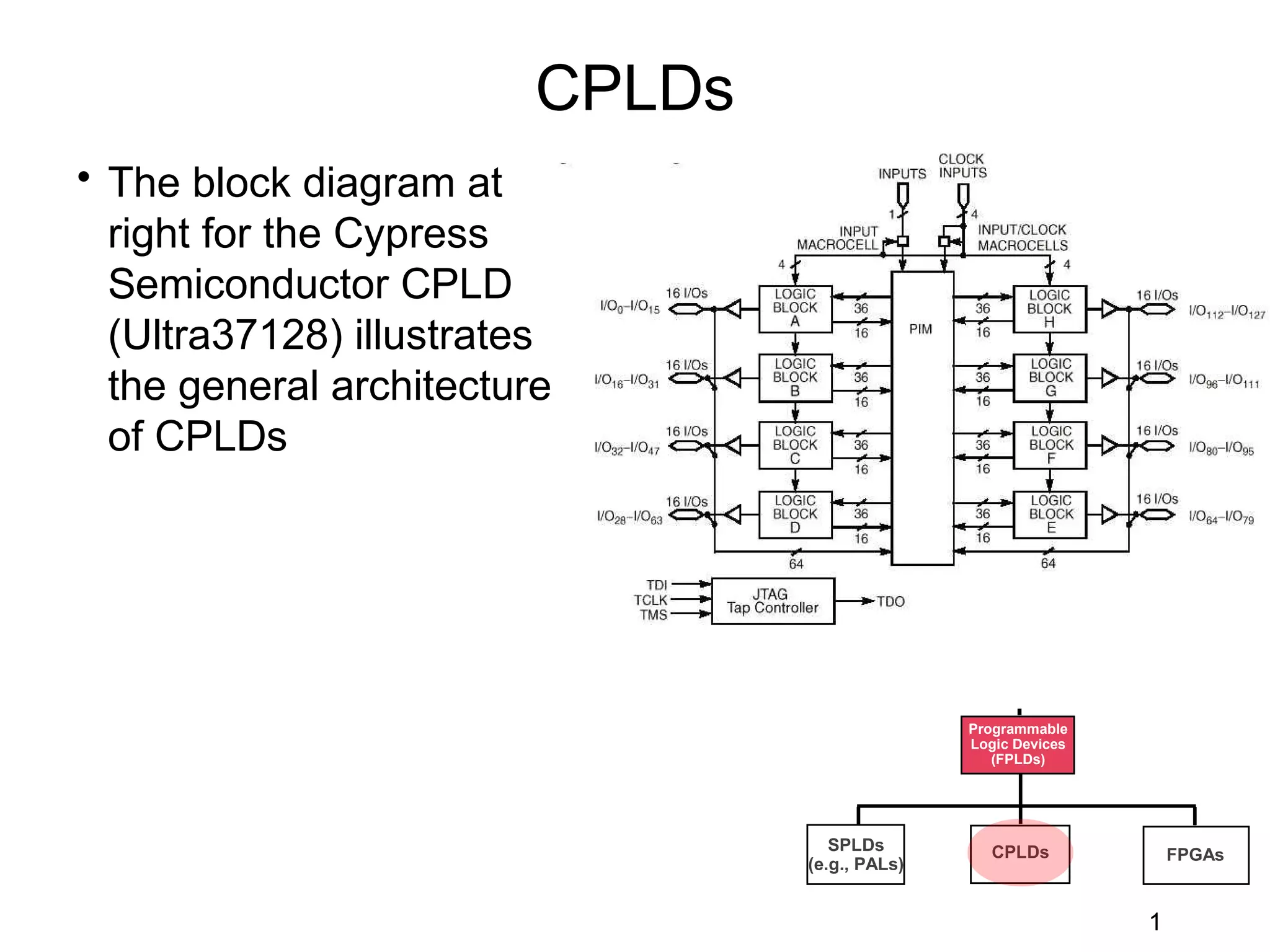
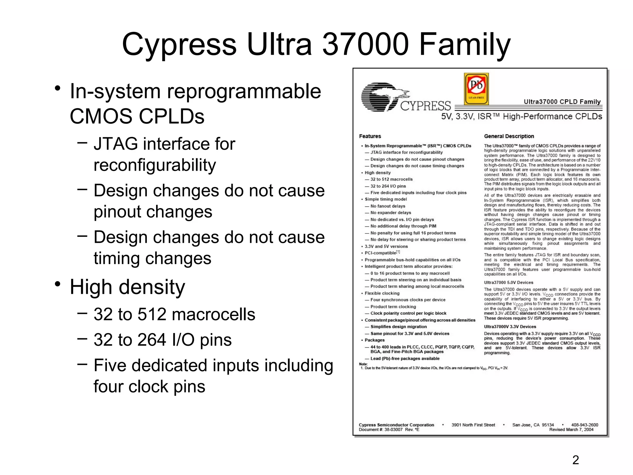
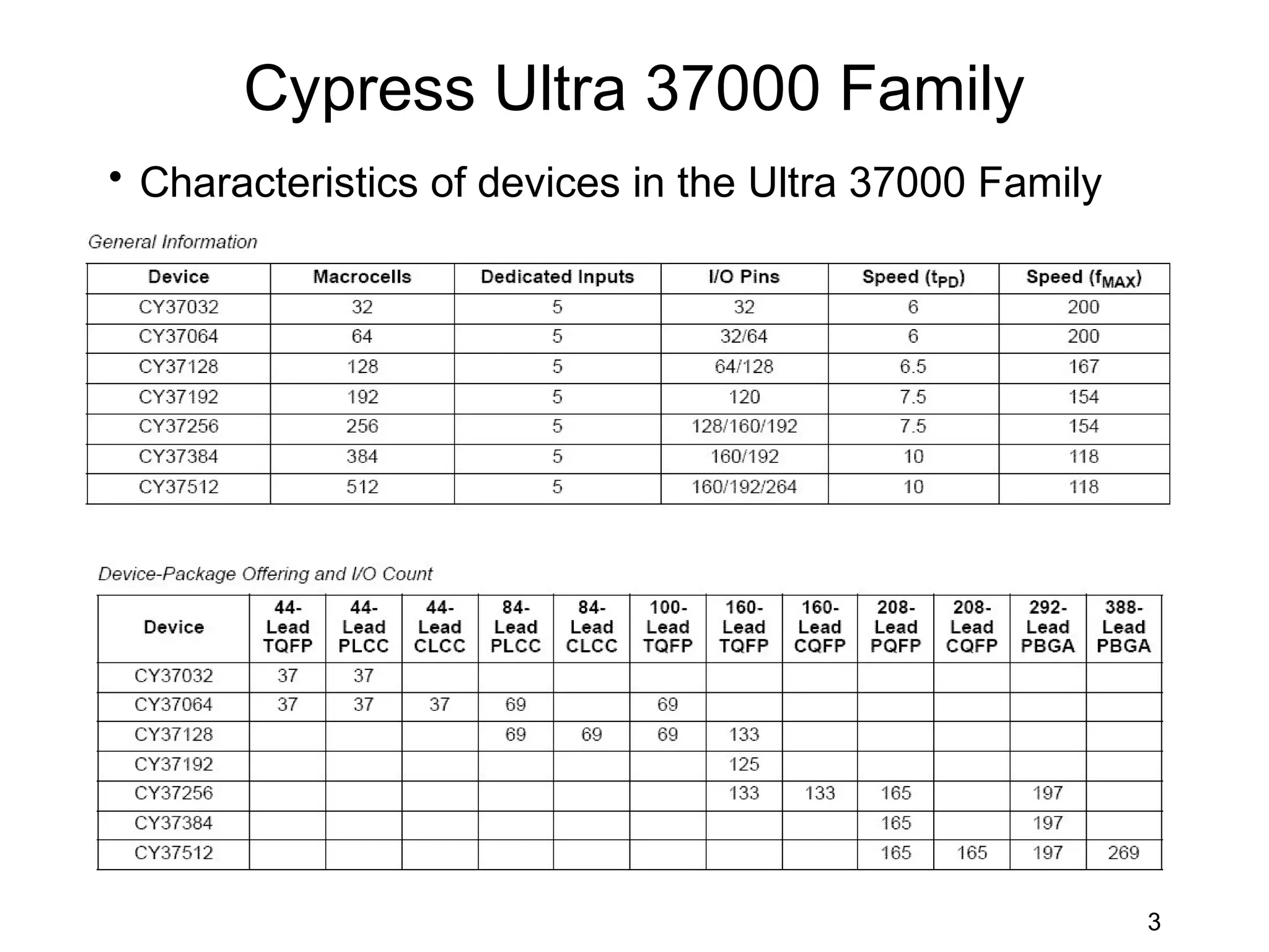
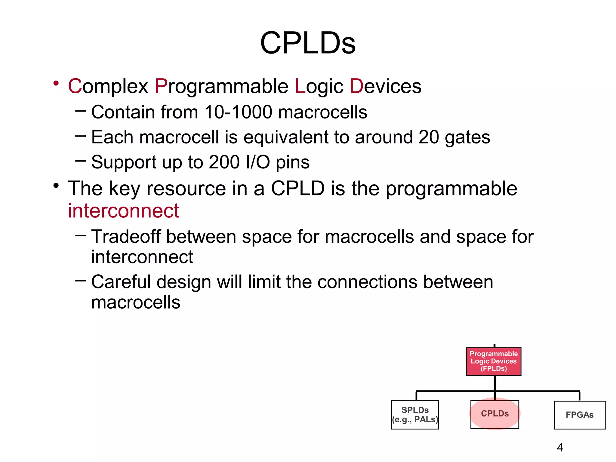
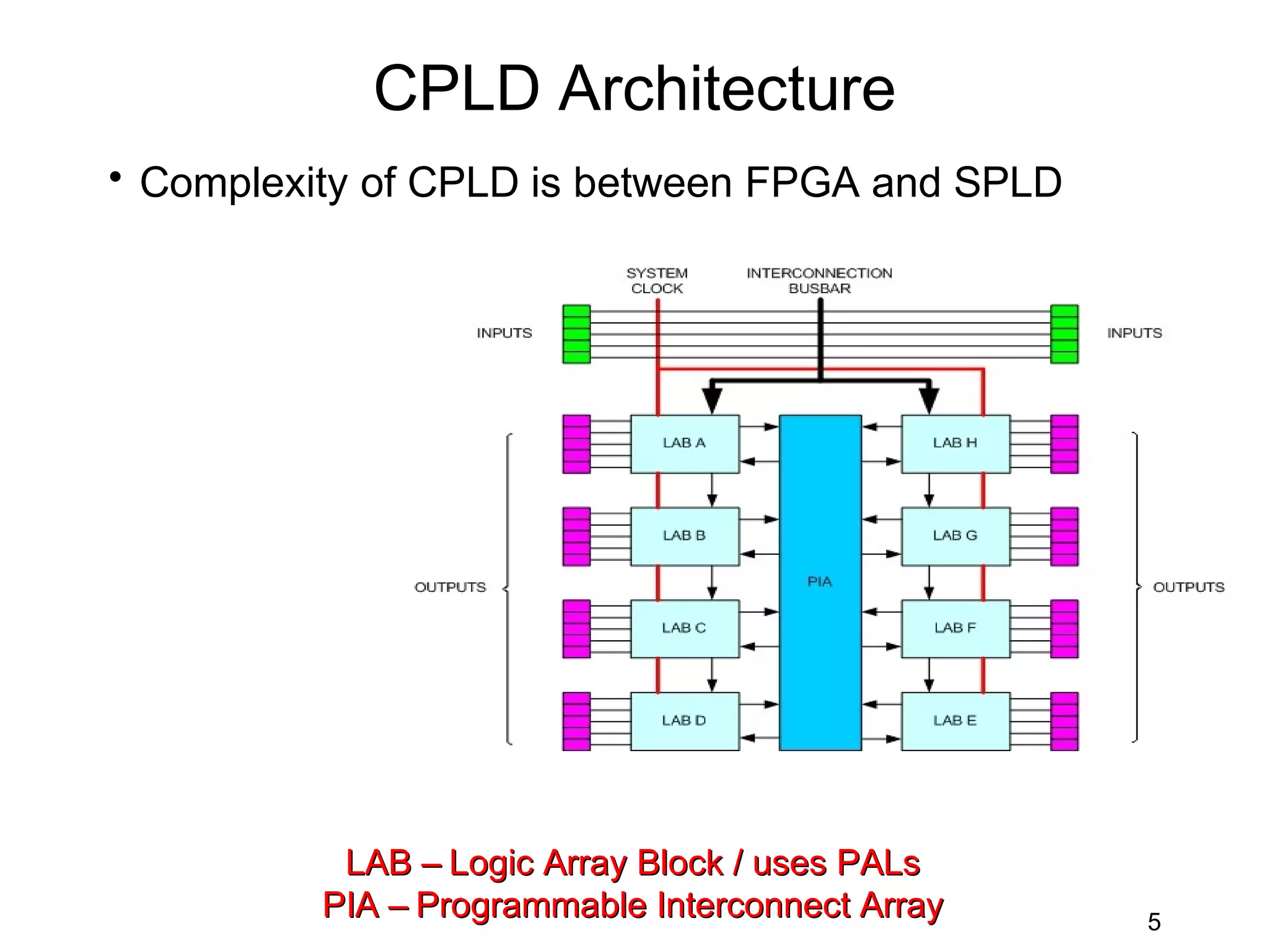
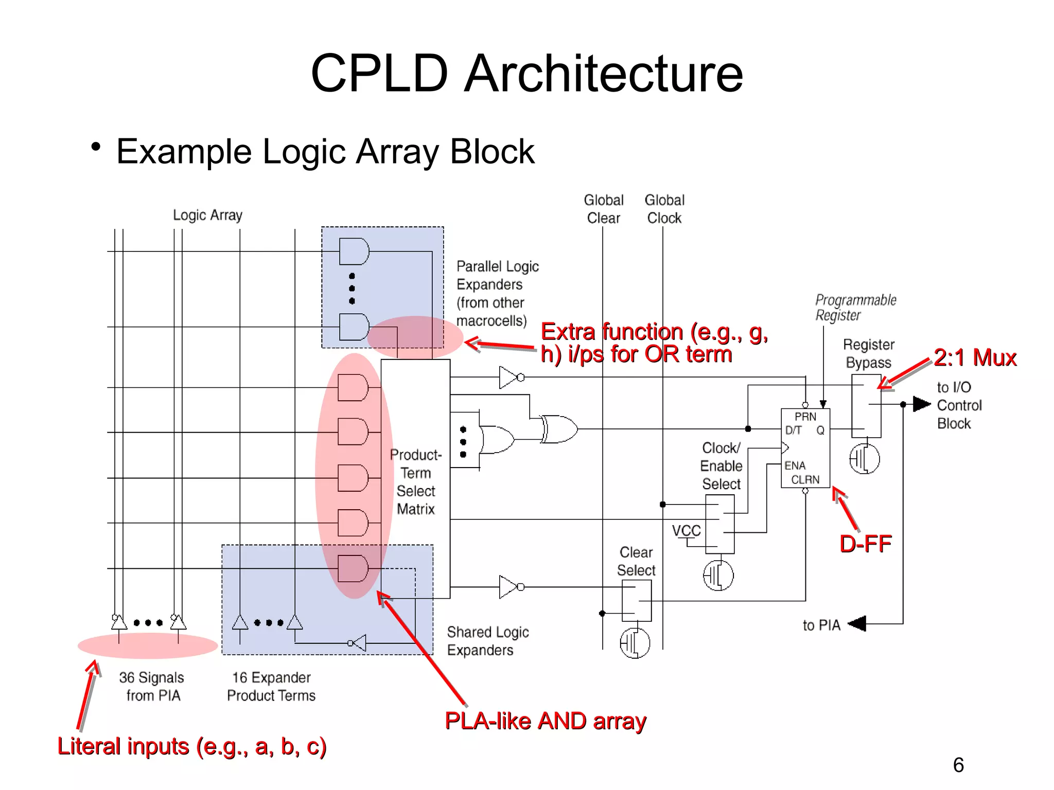
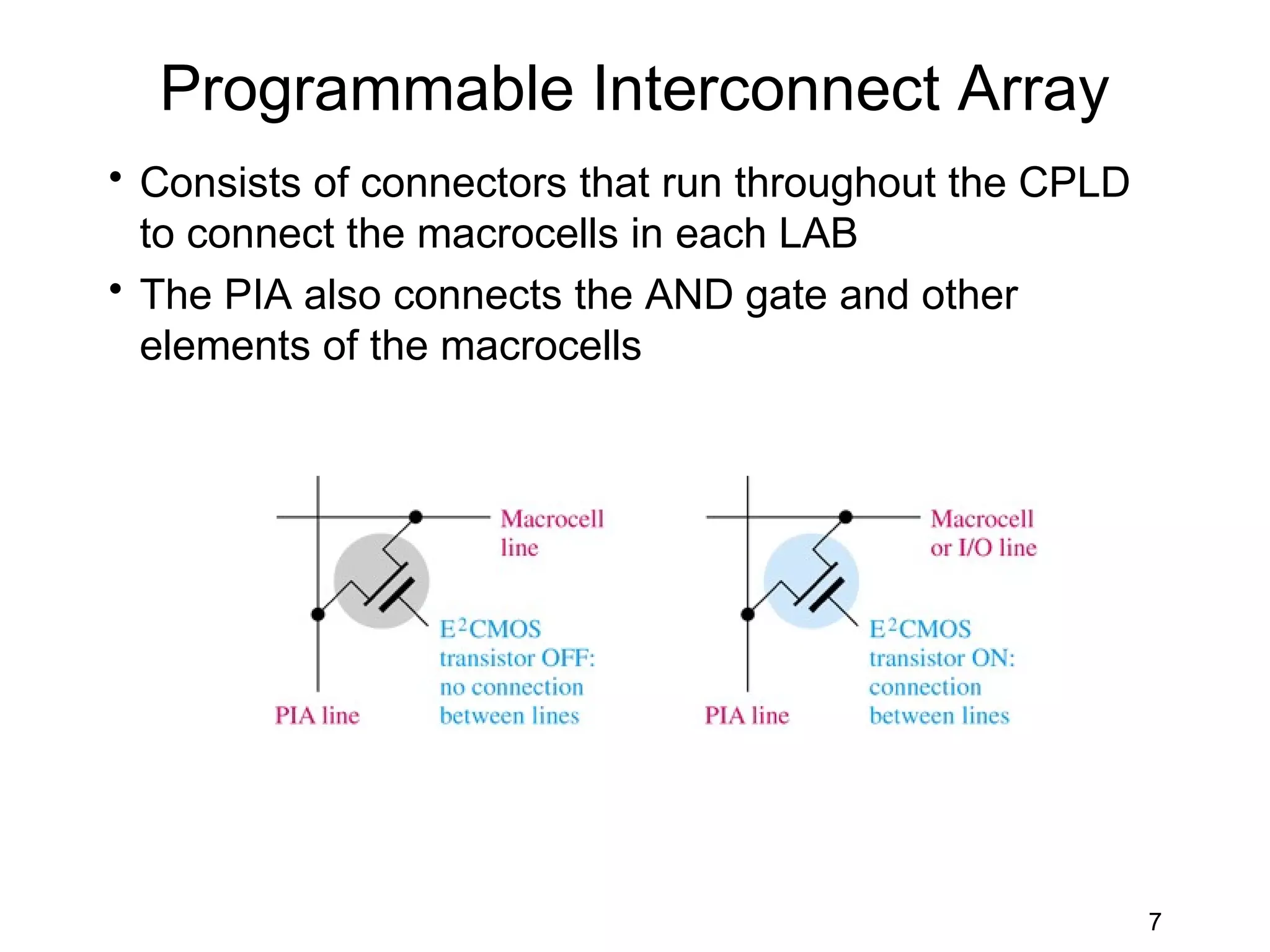
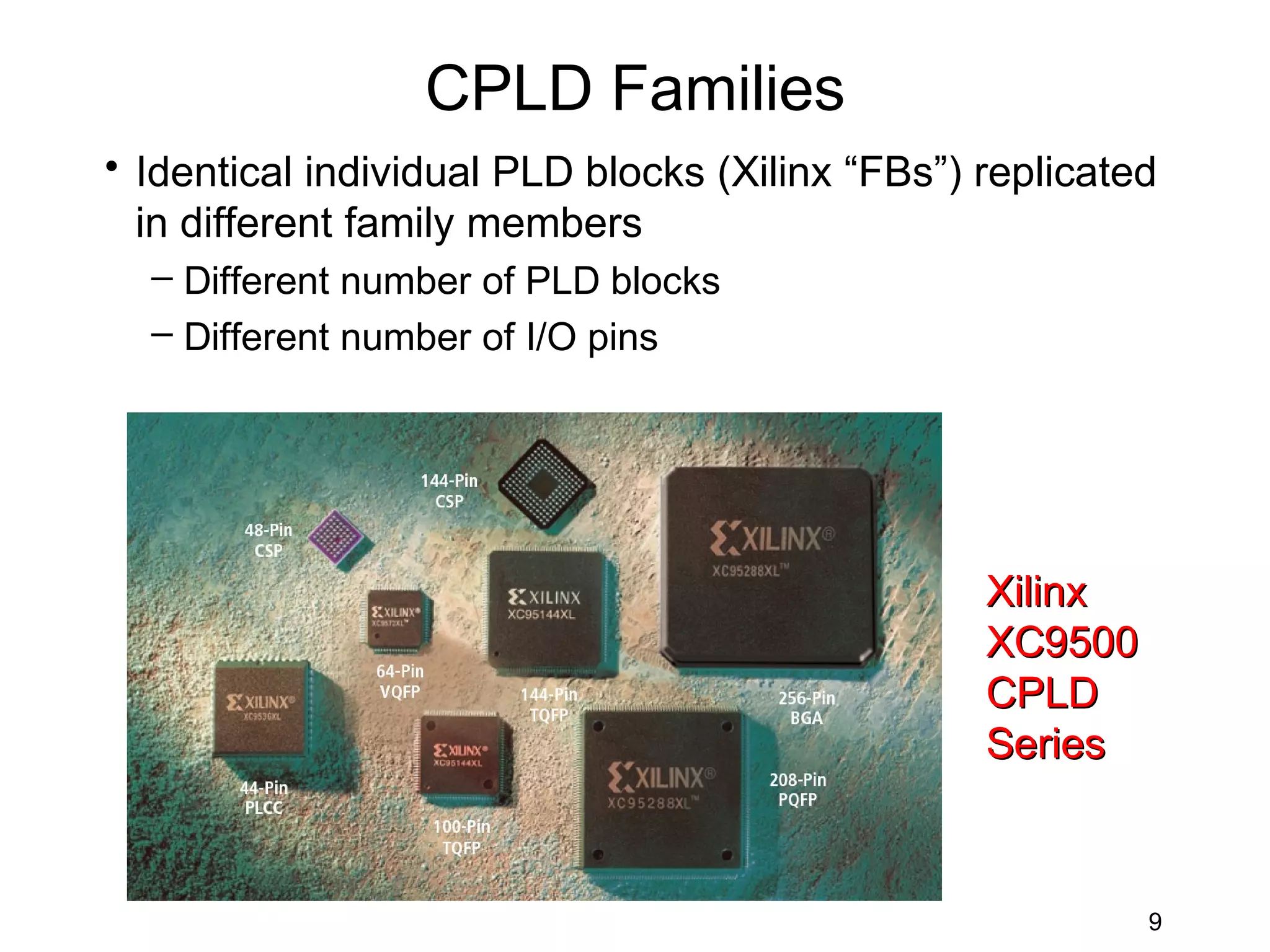
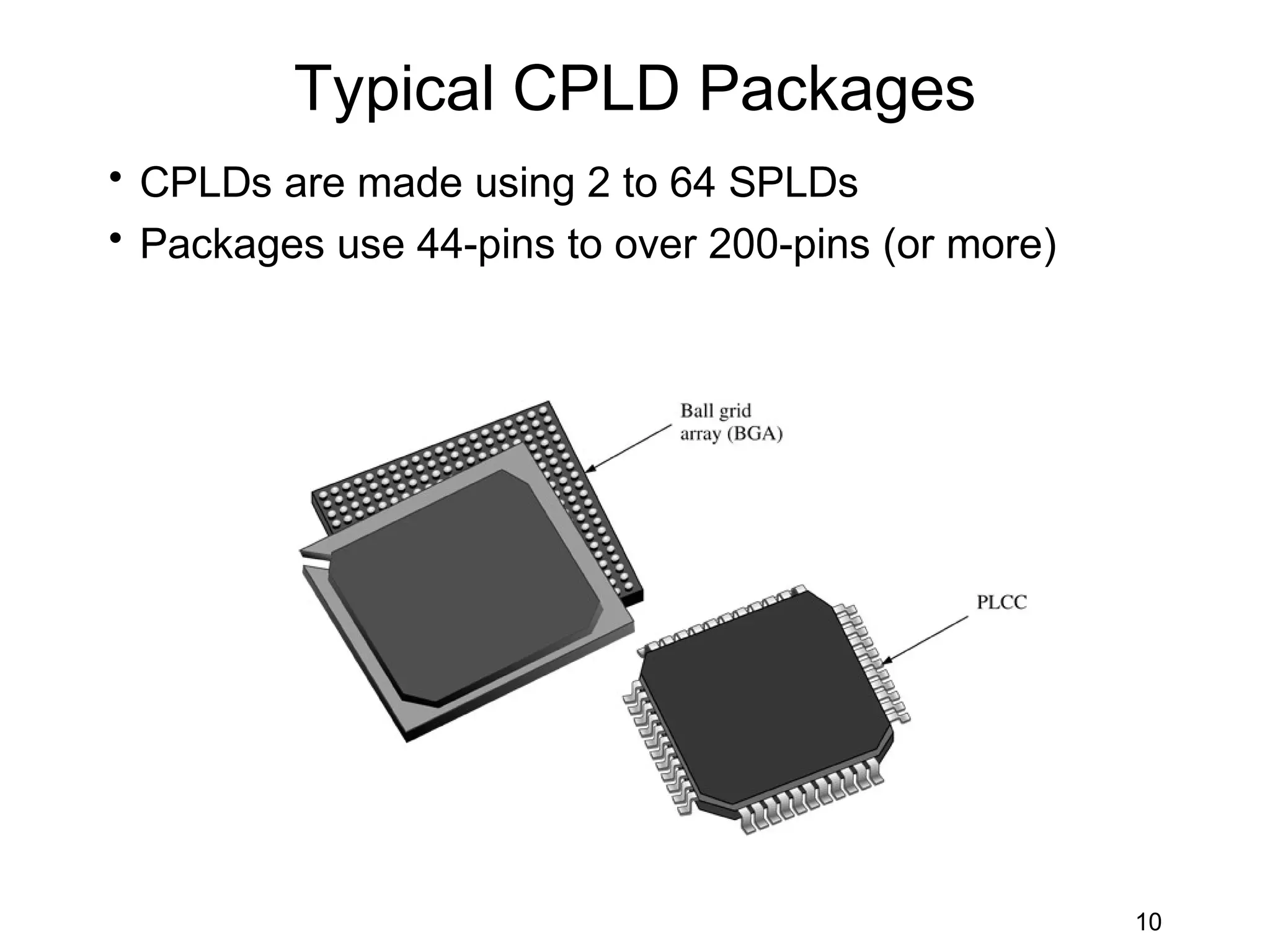
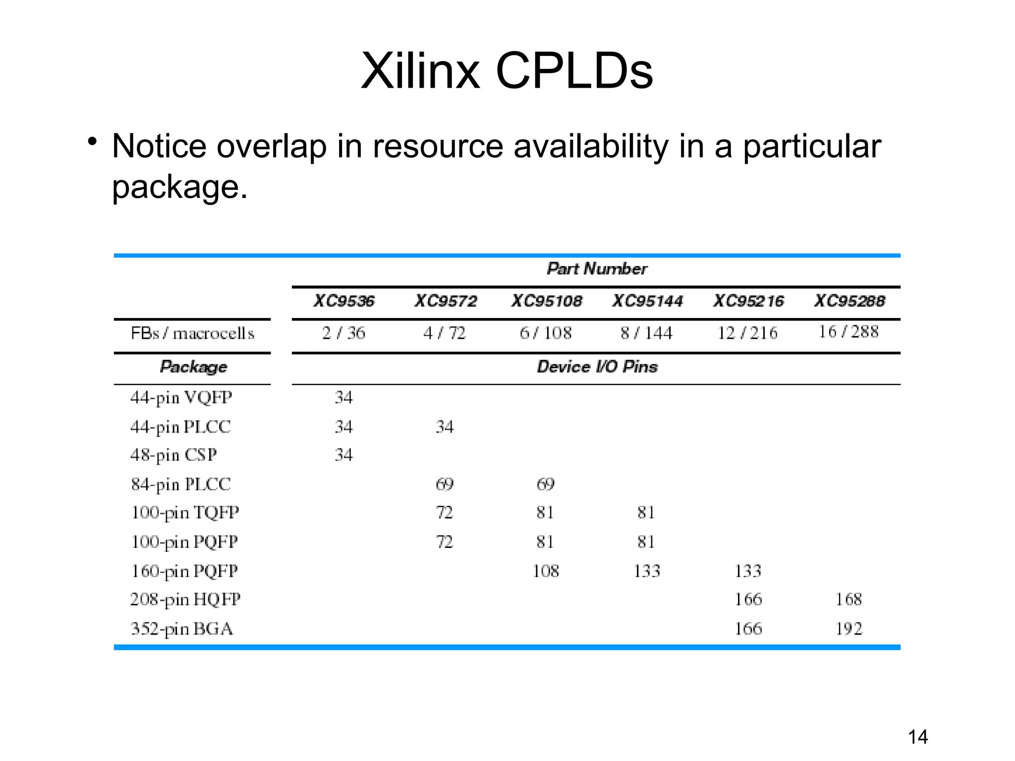
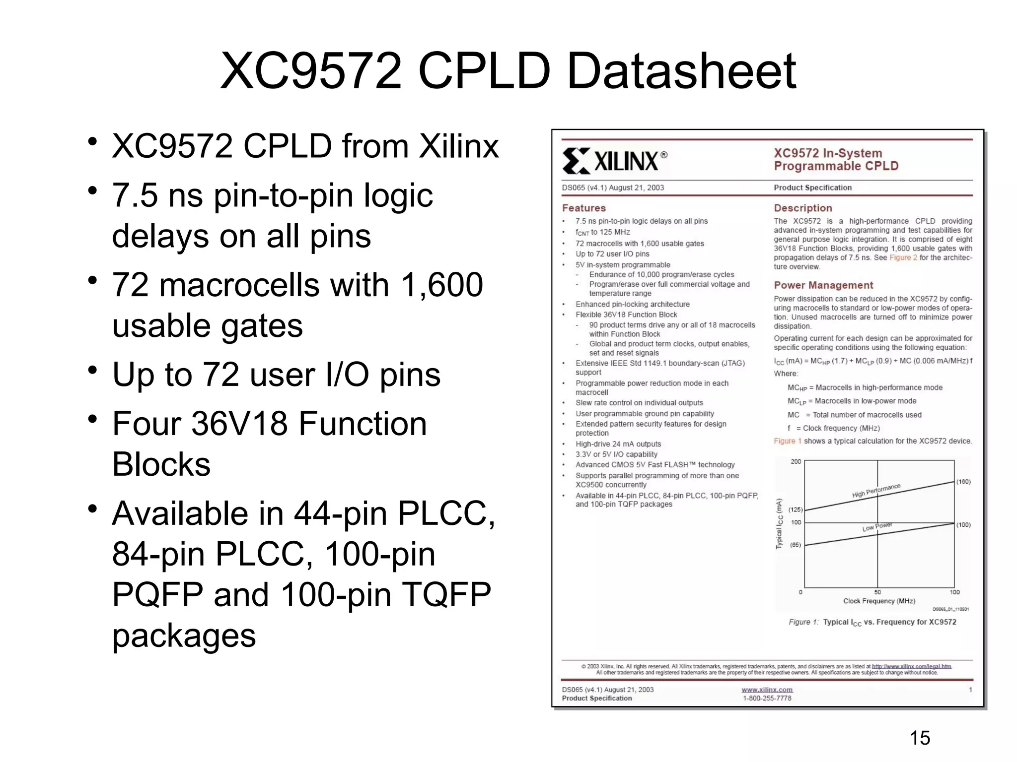
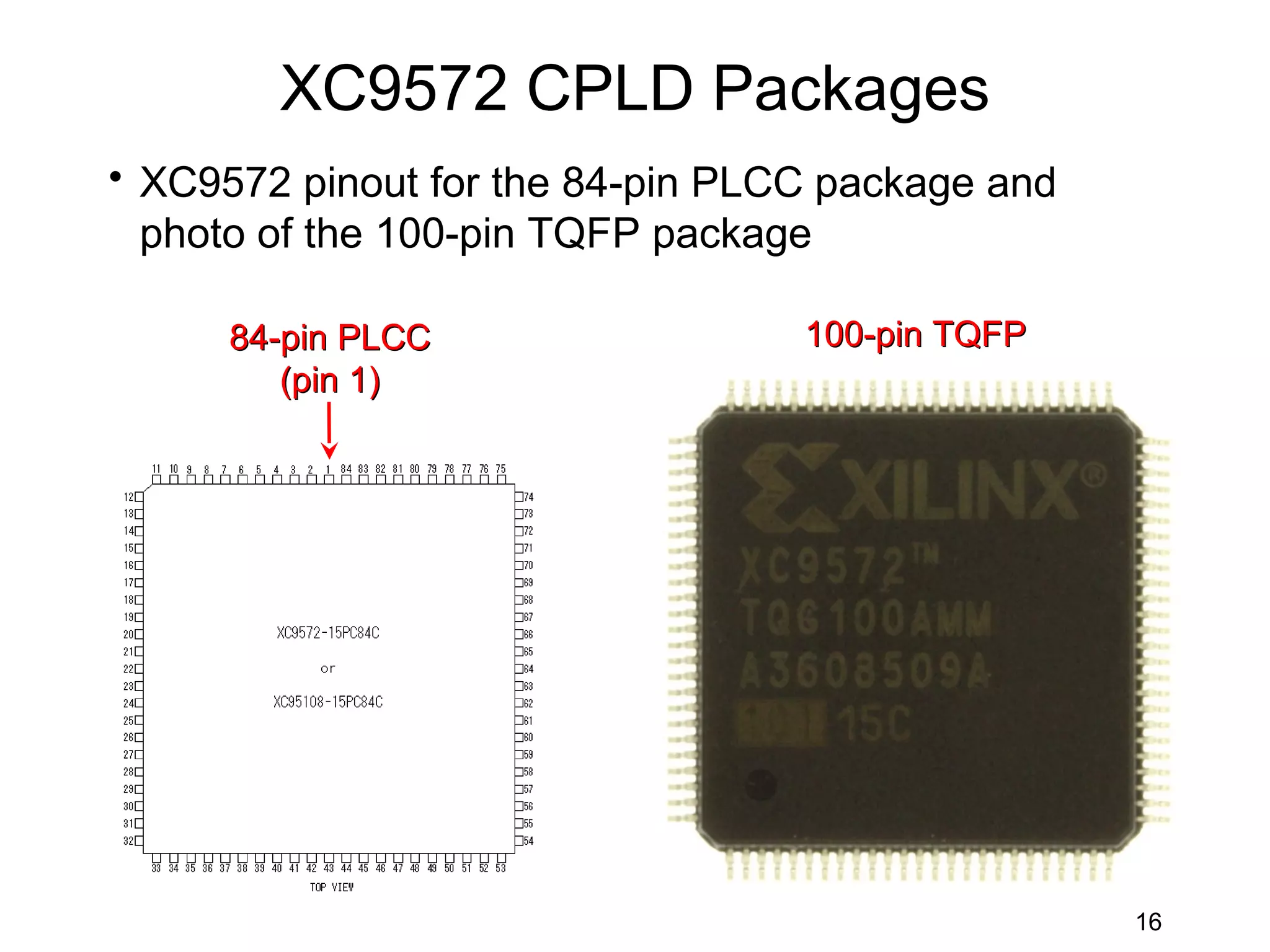
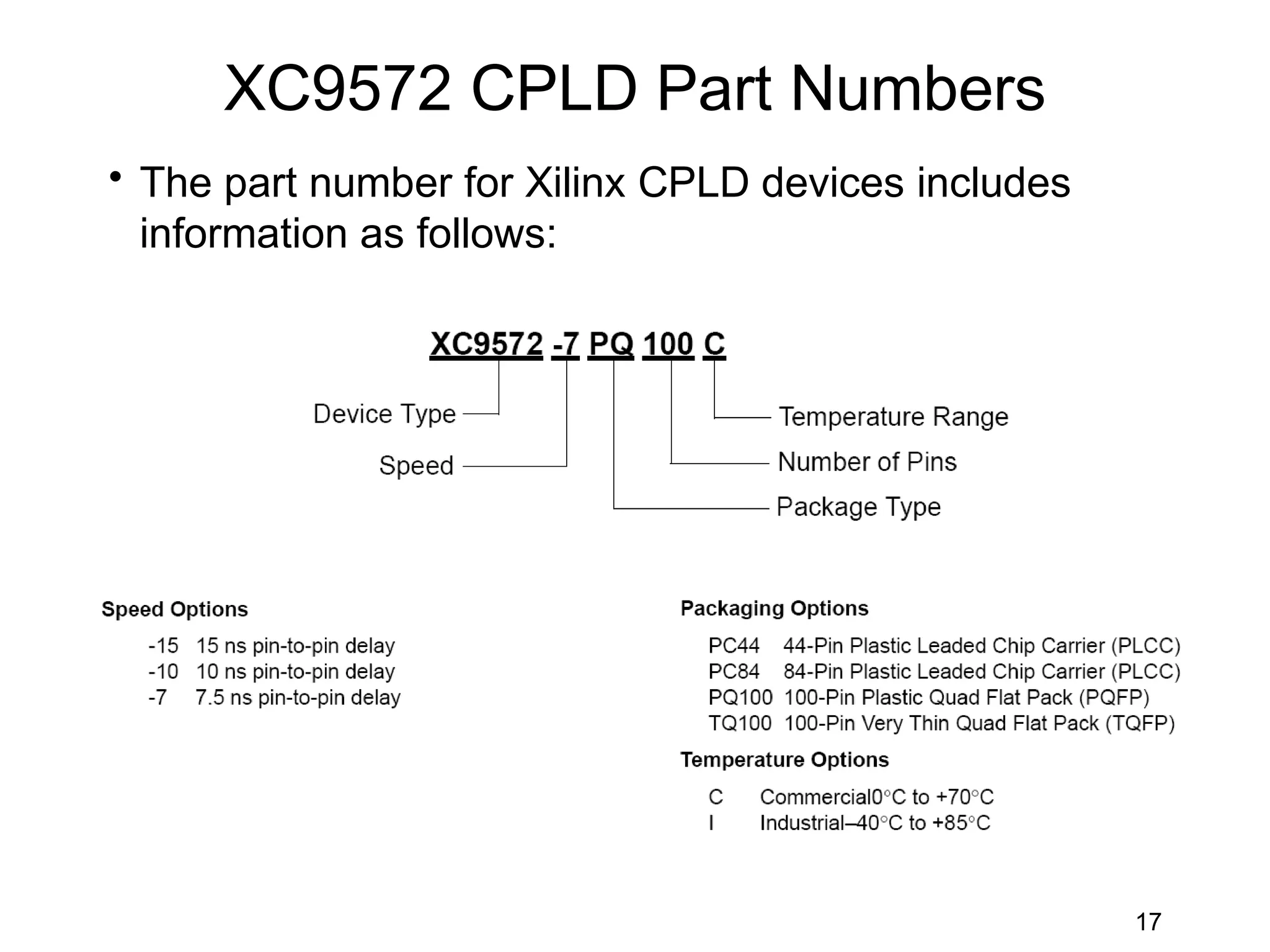
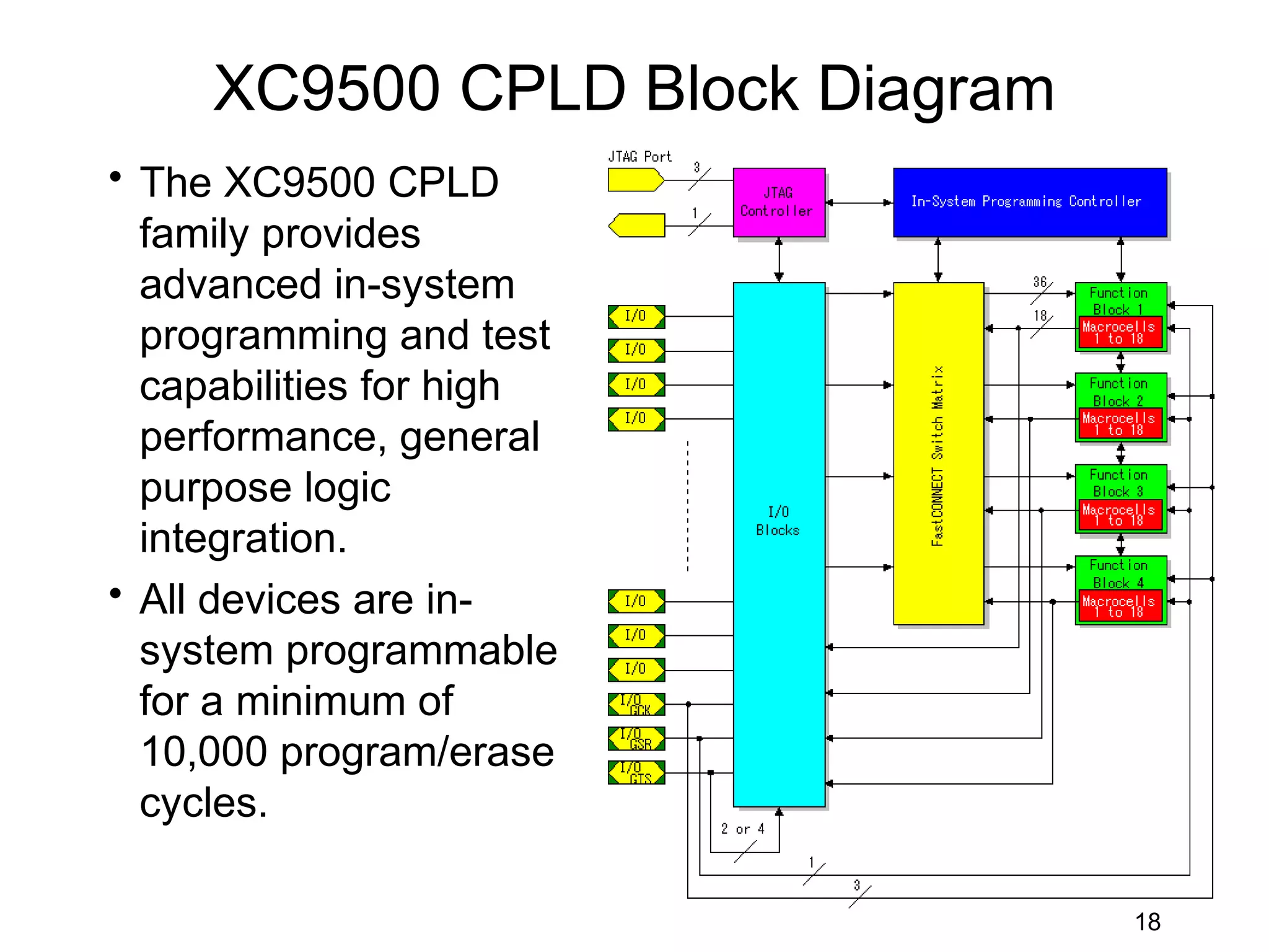
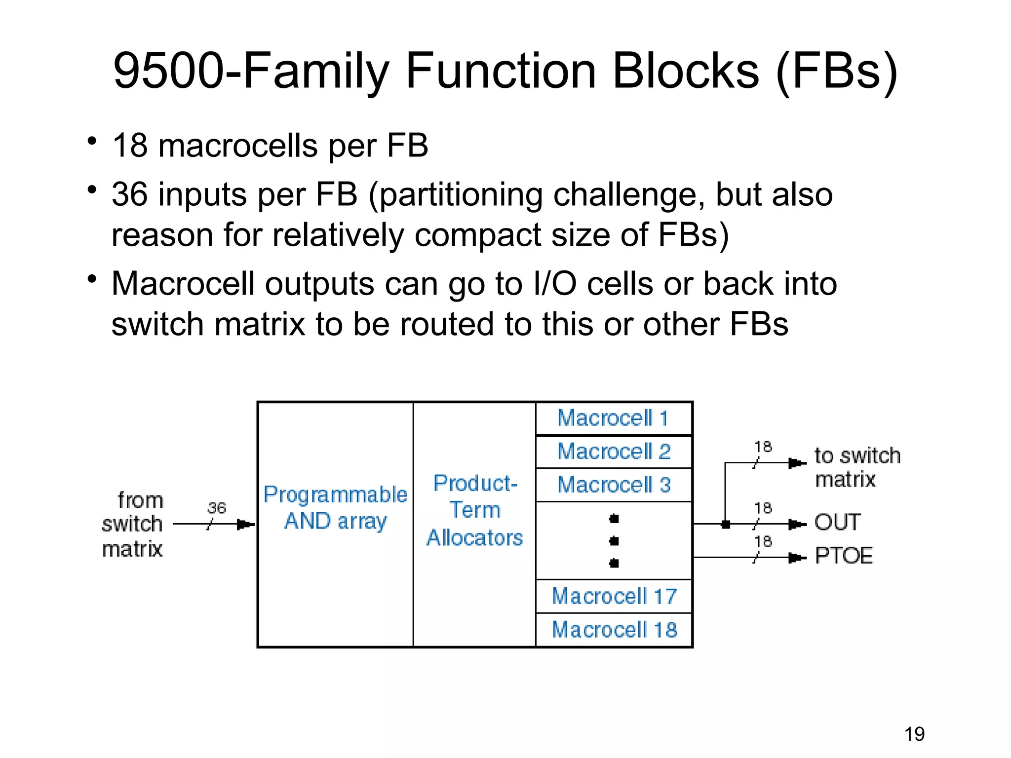
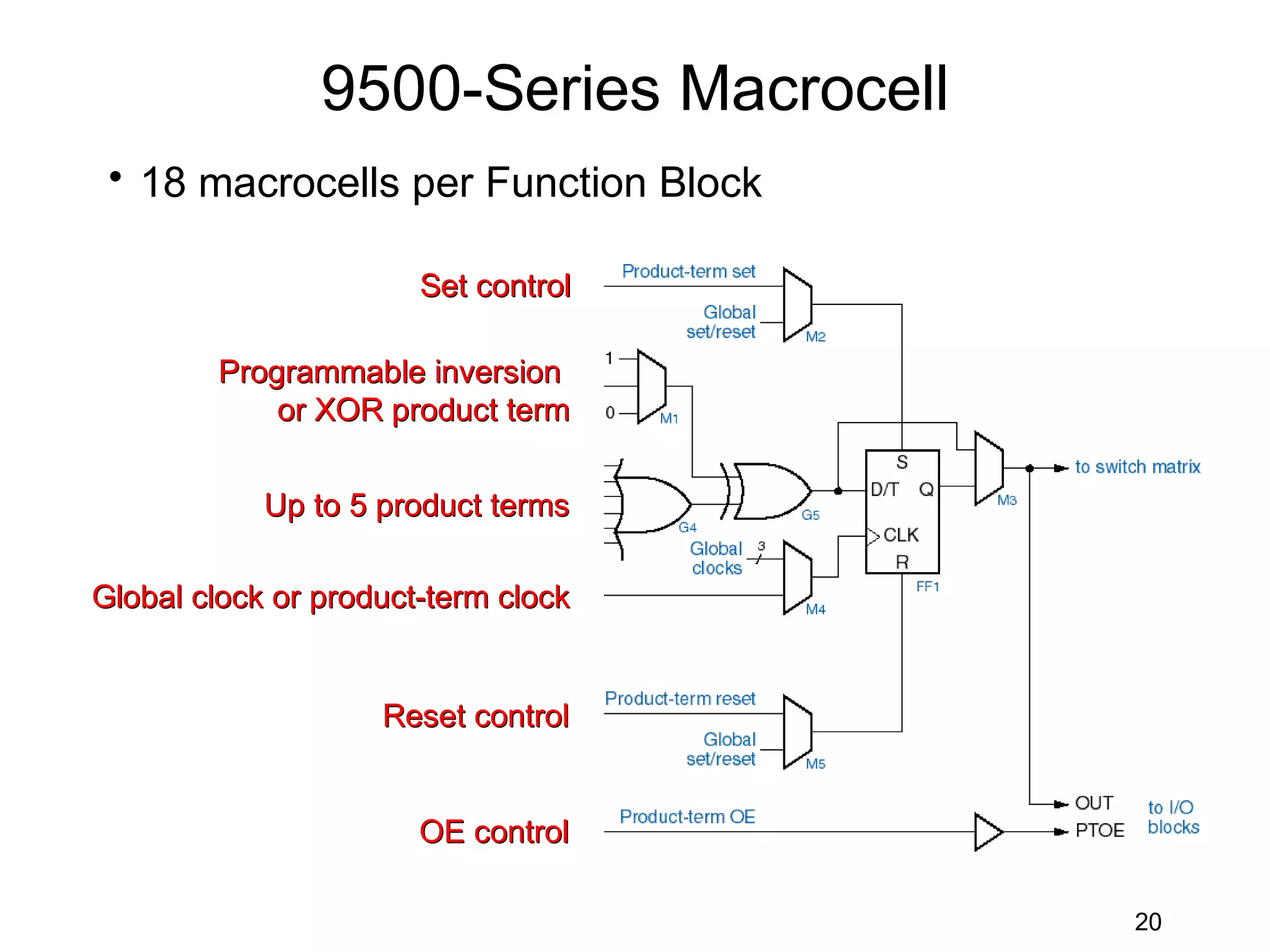
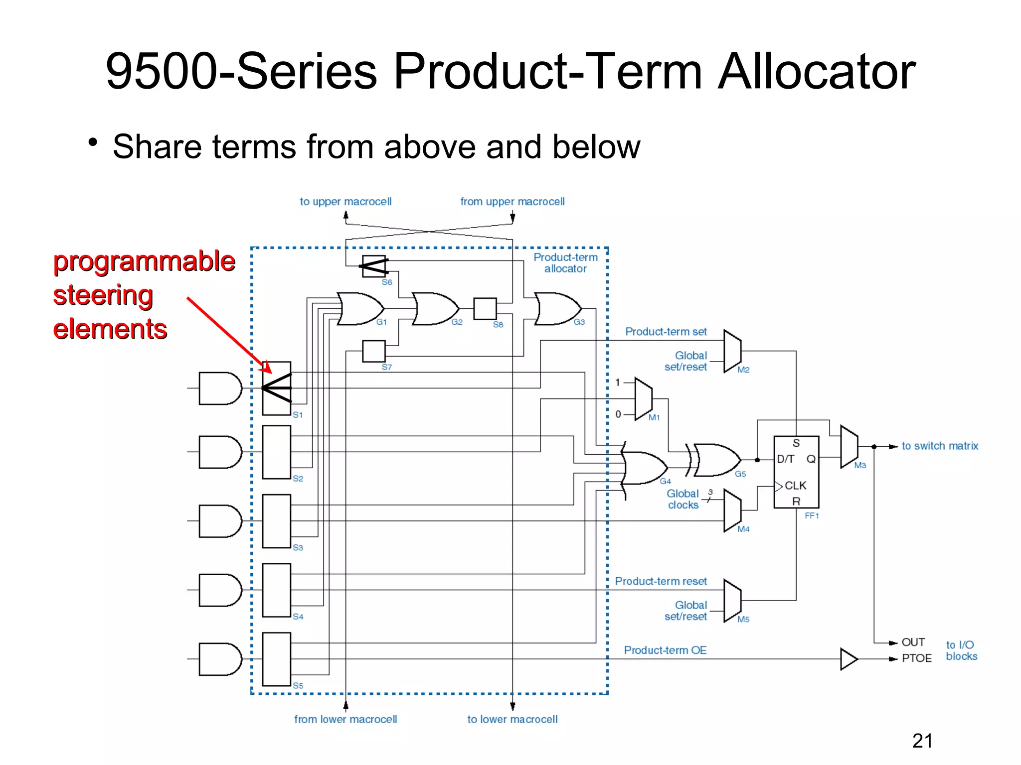
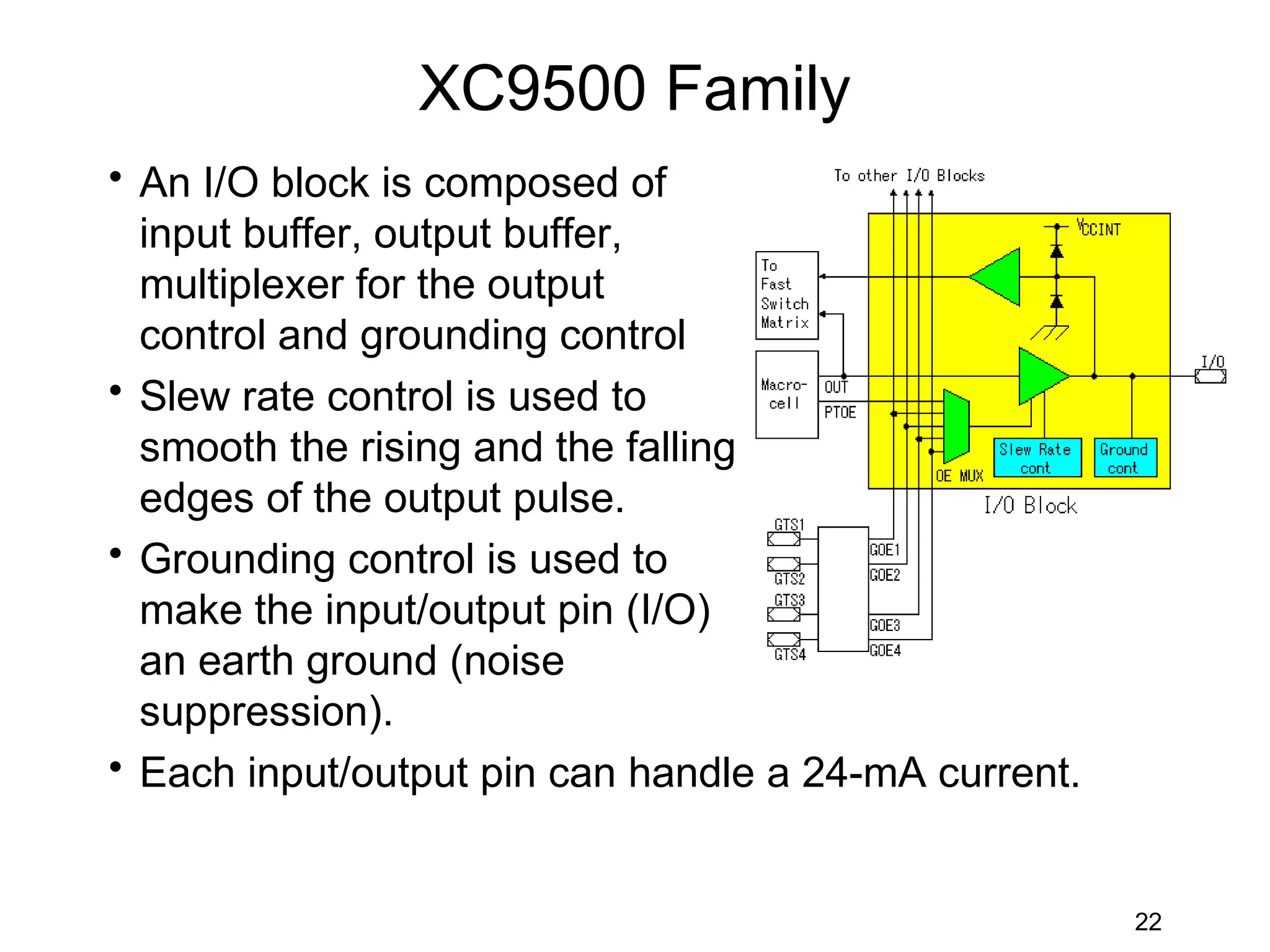
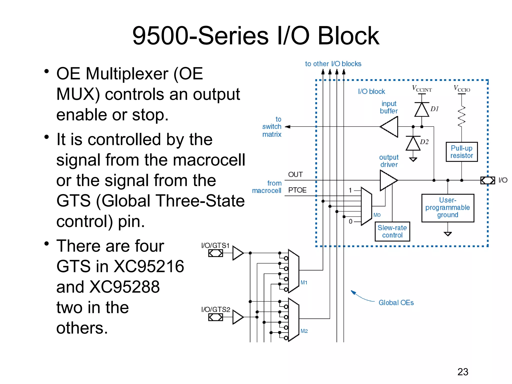
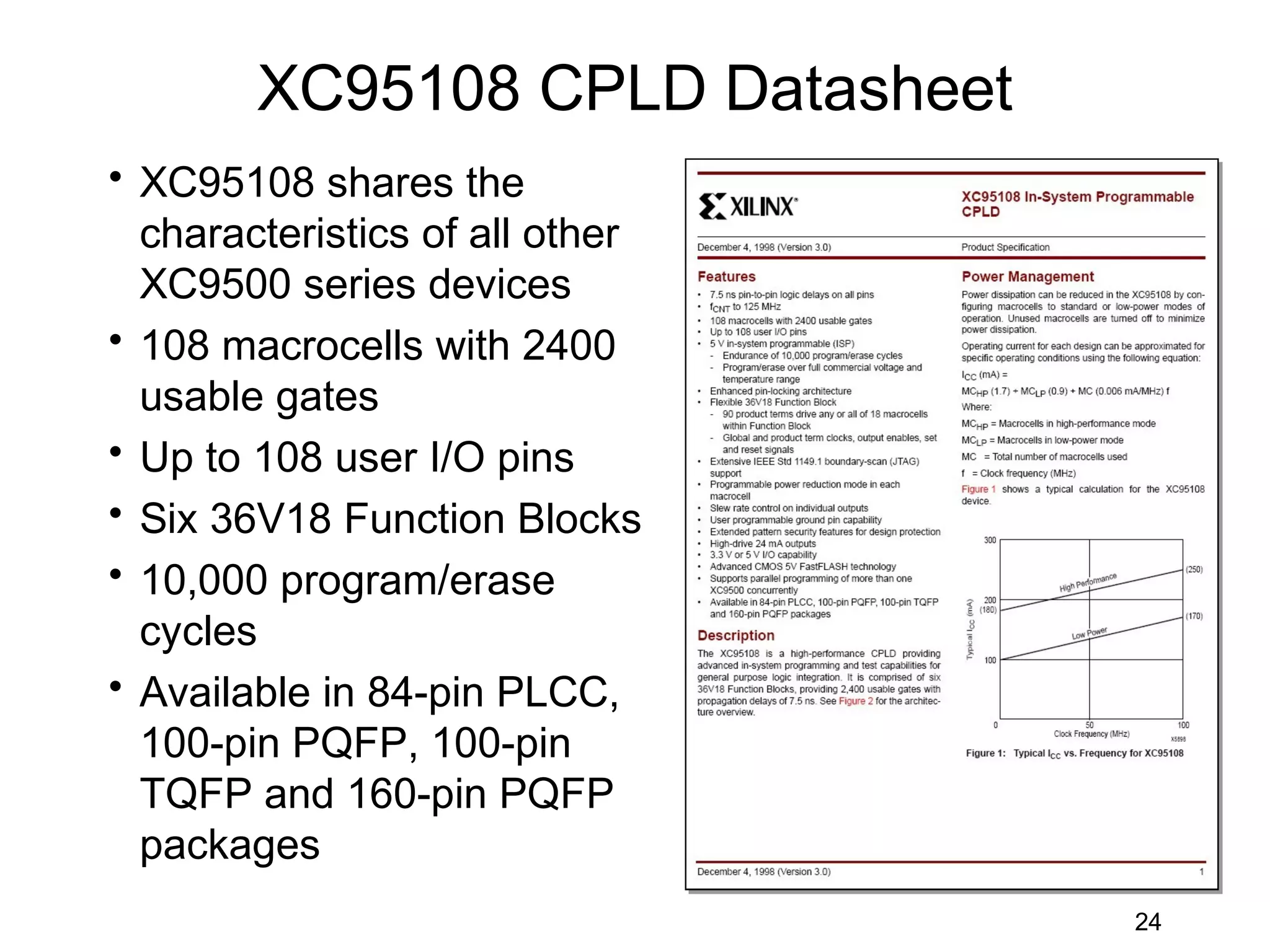
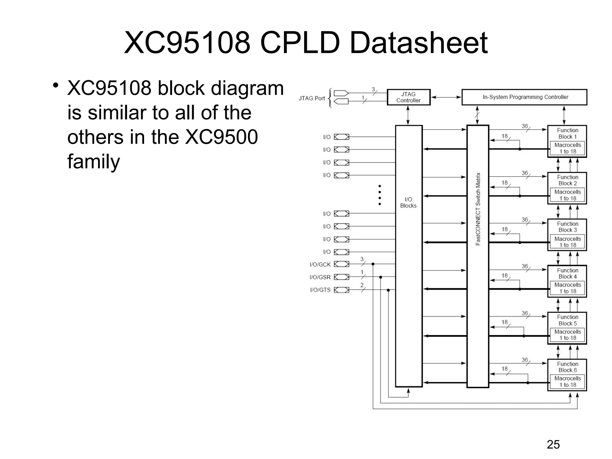
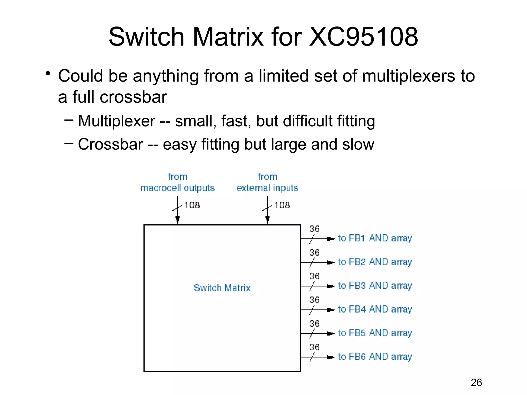
CPLDs
• The block diagram at
  right for the Cypress
  Semiconductor CPLD
  (Ultra37128) illustrates
  the general architecture
  of CPLDs


                                                Programmable
                                                Logic Devices
                                                   (FPLDs)


                                    SPLDs          CPLDs            FPGAs
                                 (e.g., PALs)


                                                                1
Cypress Ultra 37000 Family
• In-system reprogrammable
  CMOS CPLDs
  – JTAG interface for
    reconfigurability
  – Design changes do not cause
    pinout changes
  – Design changes do not cause
    timing changes
• High density
  – 32 to 512 macrocells
  – 32 to 264 I/O pins
  – Five dedicated inputs including
    four clock pins


                                      2
Cypress Ultra 37000 Family
• Characteristics of devices in the Ultra 37000 Family


                                                         3
CPLDs
• Complex Programmable Logic Devices
  – Contain from 10-1000 macrocells
  – Each macrocell is equivalent to around 20 gates
  – Support up to 200 I/O pins
• The key resource in a CPLD is the programmable
  interconnect
  – Tradeoff between space for macrocells and space for
    interconnect
  – Careful design will limit the connections between
    macrocells

                                                      Programmable
                                                      Logic Devices
                                                         (FPLDs)


                                          SPLDs          CPLDs            FPGAs
                                       (e.g., PALs)


                                                                      4
CPLD Architecture
• Complexity of CPLD is between FPGA and SPLD


           LAB – Logic Array Block / uses PALs
          PIA – Programmable Interconnect Array   5
CPLD Architecture
   • Example Logic Array Block


                                         Extra function (e.g., g,
                                         h) i/ps for OR term               2:1 Mux


                                                                    D-FF


                                 PLA-like AND array
Literal inputs (e.g., a, b, c)
                                                                            6
Programmable Interconnect Array
• Consists of connectors that run throughout the CPLD
  to connect the macrocells in each LAB
• The PIA also connects the AND gate and other
  elements of the macrocells


                                                        7
CPLD/FPGA Vendors
• The main vendors


                              8
CPLD Families
• Identical individual PLD blocks (Xilinx “FBs”) replicated
  in different family members
  – Different number of PLD blocks
  – Different number of I/O pins


                                                 Xilinx
                                                 XC9500
                                                 CPLD
                                                 Series


                                                          9
Typical CPLD Packages
• CPLDs are made using 2 to 64 SPLDs
• Packages use 44-pins to over 200-pins (or more)


                                                    10
Typical CPLD Packages
• QFP = Quad Flat Package
– A QFP is an IC package with leads extending from each of
  the four sides.
– It is used primarily for surface mounting, no socketing
• TQFP = Thin Quad Flat Package
• PQFP = Plastic Quad Flat Package
• VQFP = Very small Quad Flat Package

• PLCC = Plastic Leaded Chip Carrier
– A package related to QFP
– Similar but has pins with larger distance, curved up
  underneath a thicker body to simplify socketing

                                                         11
CPLD Package Types
• CSP = Chip Scale Package
  – IC package with an area no greater than 1.2 times that
    of the die


• BGA = Ball Grid Array
  – A type of surface-mount packaging used for ICs
  – Pins are replaced by balls of solder stuck to the bottom
    of the package
  – The device is placed on a PCB that carries copper pads
    in a pattern that matches the solder balls
  – The assembly is then heated causing the solder balls to
    melt


                                                             12
CPLD Families
• Many CPLDs have fewer
  I/O pins than macrocells
  – “Buried” Macrocells – provide
    needed logic terms internally
    but these outputs are not
    connected externally
  – IC package size dictates
    number of I/O pins but not
    the total number of
    macrocells
  – Typical CPLD families have devices with differing
    resources in the same IC package


                                                        13
Xilinx CPLDs
• Notice overlap in resource availability in a particular
  package.


                                                            14
XC9572 CPLD Datasheet
• XC9572 CPLD from Xilinx
• 7.5 ns pin-to-pin logic
  delays on all pins
• 72 macrocells with 1,600
  usable gates
• Up to 72 user I/O pins
• Four 36V18 Function
  Blocks
• Available in 44-pin PLCC,
  84-pin PLCC, 100-pin
  PQFP and 100-pin TQFP
  packages

                                15
XC9572 CPLD Packages
• XC9572 pinout for the 84-pin PLCC package and
  photo of the 100-pin TQFP package

      84-pin PLCC                 100-pin TQFP
         (pin 1)


                                                  16
XC9572 CPLD Part Numbers
• The part number for Xilinx CPLD devices includes
  information as follows:


                                                     17
XC9500 CPLD Block Diagram
• The XC9500 CPLD
  family provides
  advanced in-system
  programming and test
  capabilities for high
  performance, general
  purpose logic
  integration.
• All devices are in-
  system programmable
  for a minimum of
  10,000 program/erase
  cycles.

                                 18
9500-Family Function Blocks (FBs)
• 18 macrocells per FB
• 36 inputs per FB (partitioning challenge, but also
  reason for relatively compact size of FBs)
• Macrocell outputs can go to I/O cells or back into
  switch matrix to be routed to this or other FBs


                                                       19
9500-Series Macrocell
 • 18 macrocells per Function Block

                       Set control

        Programmable inversion
            or XOR product term


            Up to 5 product terms

Global clock or product-term clock


                    Reset control


                       OE control

                                        20
9500-Series Product-Term Allocator
  • Share terms from above and below


programmable
steering
elements


                                       21
XC9500 Family
• An I/O block is composed of
  input buffer, output buffer,
  multiplexer for the output
  control and grounding control
• Slew rate control is used to
  smooth the rising and the falling
  edges of the output pulse.
• Grounding control is used to
  make the input/output pin (I/O)
  an earth ground (noise
  suppression).
• Each input/output pin can handle a 24-mA current.


                                                      22
9500-Series I/O Block
• OE Multiplexer (OE
  MUX) controls an output
  enable or stop.
• It is controlled by the
  signal from the macrocell
  or the signal from the
  GTS (Global Three-State
  control) pin.
• There are four
  GTS in XC95216
  and XC95288
  two in the
  others.

                                   23
XC95108 CPLD Datasheet
• XC95108 shares the
  characteristics of all other
  XC9500 series devices
• 108 macrocells with 2400
  usable gates
• Up to 108 user I/O pins
• Six 36V18 Function Blocks
• 10,000 program/erase
  cycles
• Available in 84-pin PLCC,
  100-pin PQFP, 100-pin
  TQFP and 160-pin PQFP
  packages
                                 24
XC95108 CPLD Datasheet
• XC95108 block diagram
  is similar to all of the
  others in the XC9500
  family


                                 25
Switch Matrix for XC95108
• Could be anything from a limited set of multiplexers to
  a full crossbar
  – Multiplexer -- small, fast, but difficult fitting
  – Crossbar -- easy fitting but large and slow


                                                        26
Problems with CPLDs
• Pin locking
  – Small changes, and certainly large ones, can cause the
    fitter to pick a different allocation of I/O blocks and pinout
  – Locking too early may make the resulting circuit slower
    or not fit at all
• Running out of resources
  – Design may “blow up” if it doesn’t all fit on a single
    device
  – On-chip interconnect resources are much richer than off-
    chip
  – Larger devices are exponentially more expensive


                                                                27

CPLDs

  • 1.
    CPLDs • The blockdiagram at right for the Cypress Semiconductor CPLD (Ultra37128) illustrates the general architecture of CPLDs Programmable Logic Devices (FPLDs) SPLDs CPLDs FPGAs (e.g., PALs) 1
  • 2.
    Cypress Ultra 37000Family • In-system reprogrammable CMOS CPLDs – JTAG interface for reconfigurability – Design changes do not cause pinout changes – Design changes do not cause timing changes • High density – 32 to 512 macrocells – 32 to 264 I/O pins – Five dedicated inputs including four clock pins 2
  • 3.
    Cypress Ultra 37000Family • Characteristics of devices in the Ultra 37000 Family 3
  • 4.
    CPLDs • Complex ProgrammableLogic Devices – Contain from 10-1000 macrocells – Each macrocell is equivalent to around 20 gates – Support up to 200 I/O pins • The key resource in a CPLD is the programmable interconnect – Tradeoff between space for macrocells and space for interconnect – Careful design will limit the connections between macrocells Programmable Logic Devices (FPLDs) SPLDs CPLDs FPGAs (e.g., PALs) 4
  • 5.
    CPLD Architecture • Complexityof CPLD is between FPGA and SPLD LAB – Logic Array Block / uses PALs PIA – Programmable Interconnect Array 5
  • 6.
    CPLD Architecture • Example Logic Array Block Extra function (e.g., g, h) i/ps for OR term 2:1 Mux D-FF PLA-like AND array Literal inputs (e.g., a, b, c) 6
  • 7.
    Programmable Interconnect Array •Consists of connectors that run throughout the CPLD to connect the macrocells in each LAB • The PIA also connects the AND gate and other elements of the macrocells 7
  • 8.
  • 9.
    CPLD Families • Identicalindividual PLD blocks (Xilinx “FBs”) replicated in different family members – Different number of PLD blocks – Different number of I/O pins Xilinx XC9500 CPLD Series 9
  • 10.
    Typical CPLD Packages •CPLDs are made using 2 to 64 SPLDs • Packages use 44-pins to over 200-pins (or more) 10
  • 11.
    Typical CPLD Packages •QFP = Quad Flat Package – A QFP is an IC package with leads extending from each of the four sides. – It is used primarily for surface mounting, no socketing • TQFP = Thin Quad Flat Package • PQFP = Plastic Quad Flat Package • VQFP = Very small Quad Flat Package • PLCC = Plastic Leaded Chip Carrier – A package related to QFP – Similar but has pins with larger distance, curved up underneath a thicker body to simplify socketing 11
  • 12.
    CPLD Package Types •CSP = Chip Scale Package – IC package with an area no greater than 1.2 times that of the die • BGA = Ball Grid Array – A type of surface-mount packaging used for ICs – Pins are replaced by balls of solder stuck to the bottom of the package – The device is placed on a PCB that carries copper pads in a pattern that matches the solder balls – The assembly is then heated causing the solder balls to melt 12
  • 13.
    CPLD Families • ManyCPLDs have fewer I/O pins than macrocells – “Buried” Macrocells – provide needed logic terms internally but these outputs are not connected externally – IC package size dictates number of I/O pins but not the total number of macrocells – Typical CPLD families have devices with differing resources in the same IC package 13
  • 14.
    Xilinx CPLDs • Noticeoverlap in resource availability in a particular package. 14
  • 15.
    XC9572 CPLD Datasheet •XC9572 CPLD from Xilinx • 7.5 ns pin-to-pin logic delays on all pins • 72 macrocells with 1,600 usable gates • Up to 72 user I/O pins • Four 36V18 Function Blocks • Available in 44-pin PLCC, 84-pin PLCC, 100-pin PQFP and 100-pin TQFP packages 15
  • 16.
    XC9572 CPLD Packages •XC9572 pinout for the 84-pin PLCC package and photo of the 100-pin TQFP package 84-pin PLCC 100-pin TQFP (pin 1) 16
  • 17.
    XC9572 CPLD PartNumbers • The part number for Xilinx CPLD devices includes information as follows: 17
  • 18.
    XC9500 CPLD BlockDiagram • The XC9500 CPLD family provides advanced in-system programming and test capabilities for high performance, general purpose logic integration. • All devices are in- system programmable for a minimum of 10,000 program/erase cycles. 18
  • 19.
    9500-Family Function Blocks(FBs) • 18 macrocells per FB • 36 inputs per FB (partitioning challenge, but also reason for relatively compact size of FBs) • Macrocell outputs can go to I/O cells or back into switch matrix to be routed to this or other FBs 19
  • 20.
    9500-Series Macrocell •18 macrocells per Function Block Set control Programmable inversion or XOR product term Up to 5 product terms Global clock or product-term clock Reset control OE control 20
  • 21.
    9500-Series Product-Term Allocator • Share terms from above and below programmable steering elements 21
  • 22.
    XC9500 Family • AnI/O block is composed of input buffer, output buffer, multiplexer for the output control and grounding control • Slew rate control is used to smooth the rising and the falling edges of the output pulse. • Grounding control is used to make the input/output pin (I/O) an earth ground (noise suppression). • Each input/output pin can handle a 24-mA current. 22
  • 23.
    9500-Series I/O Block •OE Multiplexer (OE MUX) controls an output enable or stop. • It is controlled by the signal from the macrocell or the signal from the GTS (Global Three-State control) pin. • There are four GTS in XC95216 and XC95288 two in the others. 23
  • 24.
    XC95108 CPLD Datasheet •XC95108 shares the characteristics of all other XC9500 series devices • 108 macrocells with 2400 usable gates • Up to 108 user I/O pins • Six 36V18 Function Blocks • 10,000 program/erase cycles • Available in 84-pin PLCC, 100-pin PQFP, 100-pin TQFP and 160-pin PQFP packages 24
  • 25.
    XC95108 CPLD Datasheet •XC95108 block diagram is similar to all of the others in the XC9500 family 25
  • 26.
    Switch Matrix forXC95108 • Could be anything from a limited set of multiplexers to a full crossbar – Multiplexer -- small, fast, but difficult fitting – Crossbar -- easy fitting but large and slow 26
  • 27.
    Problems with CPLDs •Pin locking – Small changes, and certainly large ones, can cause the fitter to pick a different allocation of I/O blocks and pinout – Locking too early may make the resulting circuit slower or not fit at all • Running out of resources – Design may “blow up” if it doesn’t all fit on a single device – On-chip interconnect resources are much richer than off- chip – Larger devices are exponentially more expensive 27