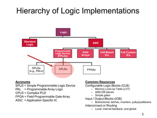
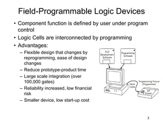
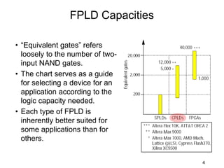
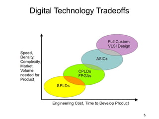
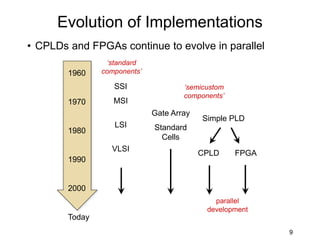
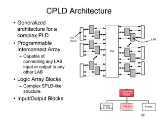
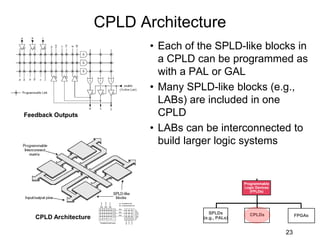
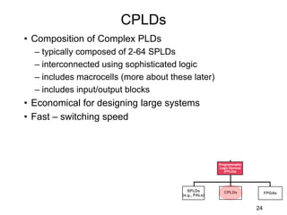
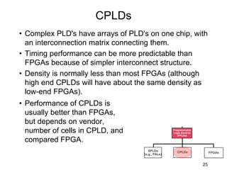
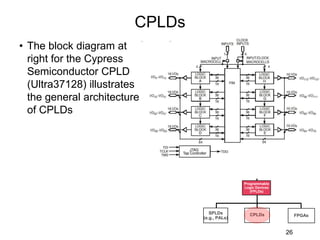
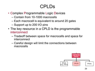
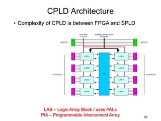
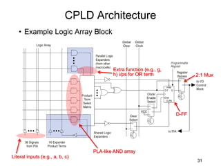
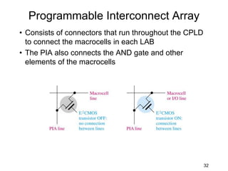
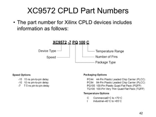
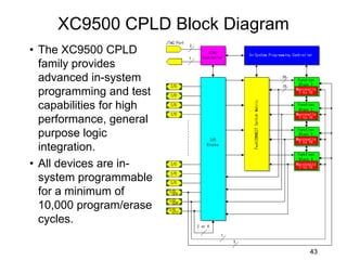
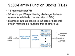
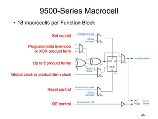
SlideShare a Scribd company logo
1 of 52
Download to read offline
• Overview of FPLDs
– History
– Tradeoffs
• CPLDs
– General Description
– Basic Architecture
• Specific Vendor Devices
– Xilinx
– Altera
• Xilinx XC9500 Series
• CPLD Problems
1
Hierarchy of Logic Implementations
Acronyms
SPLD = Simple Programmable Logic Device
PAL = Programmable Array Logic
CPLD = Complex PLD
FPGA = Field Programmable Gate Array
ASIC = Application Specific IC
Common Resources
Configurable Logic Blocks (CLB)
– Memory Look-Up Table (LUT)
– AND-OR planes
– Simple gates
Input / Output Blocks (IOB)
– Bidirectional, latches, inverters, pullup/pulldowns
Interconnect or Routing
– Local, internal feedback, and global
Logic
Standard
Logic
ASIC
Programmable
Logic Devices
(FPLDs)
Gate
Arrays
Cell-Based
ICs
Full Custom
ICs
CPLDs
SPLDs
(e.g., PALs) FPGAs
2
Field-Programmable Logic Devices
• Component function is defined by user under program
control
• Logic Cells are interconnected by programming
• Advantages:
– Flexible design that changes by
reprogramming, ease of design
changes
– Reduce prototype-product time
– Large scale integration (over
100,000 gates)
– Reliability increased, low financial
risk
– Smaller device, low start-up cost
3
FPLD Capacities
• “Equivalent gates” refers
loosely to the number of two-
input NAND gates.
• The chart serves as a guide
for selecting a device for an
application according to the
logic capacity needed.
• Each type of FPLD is
inherently better suited for
some applications than for
others.
4
Digital Technology Tradeoffs
S
5
Which Implementation Technology?
• Economic versus technical factors
– The next few slides off a comparison of economic and
technical factors associated with these technologies
6
SPLD
SSI/MSI
semicustom
technologies
standard
components
CPLD
FPGA
Gate
Array
Std.
Cell
Full
Custom
Comparison of Implementations
• The table below offers a comparison of the major
implementation technologies over four key factors
7
SSI/MSI SPLD FPGA Gate Array
Standard
Cell
Full
Custom
Gates/Component 5 - 100 50 - 5K 100 - 10K 500 - 100K 10K - 500K 100K - 10M
Cost/Gate
High Low
NRE Cost ($) - 1-2K 2-10K 5-50K 10-100K 50K-5M
Development time
(weeks)
- 1-2 1-2 2-20 5-50 20-200
Comparison of Implementations
Circuit Cost As A Function Of Volume
Discrete
Full custom
Volume
Cost
8
Evolution of Implementations
• CPLDs and FPGAs continue to evolve in parallel
9
1960
1970
1980
1990
2000
Today
SSI
MSI
LSI
VLSI
‘standard
components’
‘semicustom
components’
Gate Array
Standard
Cells
Simple PLD
CPLD FPGA
parallel
development
Three FPLD Types
• Simple Programmable Logic Device (SPLD)
– LSI device
– Less than 1000 logic gates
• Complex Programmable Logic Device (CPLD)
– VLSI device
– Higher logic capacity than SPLDs
• Field Programmable Gate Array (FPGA)
– VLSI device
– Higher logic capacity than CPLDs
10
Programmable
Logic Devices
(FPLDs)
CPLDs
SPLDs
(e.g., PALs)
FPGAs
Three FPLD Types
• Simple Programmable Logic Device (SPLD)
– PLA or PAL
– Fixed internal routing, deterministic propagation delays
• Complex Programmable Logic Device (CPLD)
– Multiple SPLDs onto a single chip
– Programmable interconnect
• Field Programmable Gate Array (FPGA)
– An array of logic blocks
– Large number of gates, user selectable interconnection,
delays depending on design and routing
– A high ratio of flip-flops to logic resources
11
Programmable
Logic Devices
(FPLDs)
CPLDs
SPLDs
(e.g., PALs)
FPGAs
SPLDs
• SPLDs = Simple PLDs
• Popular SPLD Architecture Types
– Programmable Logic Array, PLA
– Programmable Array Logic, PAL (Vantis)
– General Array Logic, GAL (Lattice)
– others
• Architecture Differences
– AND versus OR implementation
– Programmability (e.g., EE)
– Fundamental logic block
12
Programmable
Logic Devices
(FPLDs)
CPLDs
SPLDs
(e.g., PALs)
FPGAs
SPLDs
• We have already taken a close
look at SPLDs
• A PLA-like SPLD is illustrated
at left
– PAL and GAL devices offered
a somewhat better solution
• SPLDs are good alternative to
using SSI and MSI devices
– Especially if re-programmable
13
Logic Functions
Product Terms
Sums
Programmable
Logic Devices
(FPLDs)
CPLDs
SPLDs
(e.g., PALs)
FPGAs
SPLDs
• Conventional programmable logic
– PALs, PLAs, GALs
– standard parts like GAL22V10 and PAL16R4 are available from
multiple vendors
• Includes programmable logic cells to a limited degree
(programming options in I/O cells, may have fixed
AND/OR gates for logic), limited routing network
• Lowest density of all programmable devices, however,
can offer very high performance
14
Programmable
Logic Devices
(FPLDs)
CPLDs
SPLDs
(e.g., PALs)
FPGAs
• SPLDs have nearly replaced
TTL logic which was the
dominate approach to logic
implementation
15
How to Expand SPLD Architecture?
• Increase number of inputs and outputs in a
conventional PLD?
– e.g., 16V8 → 20V8 → 22V10
– Why not → 32V16 → 128V64 ?
• Problems:
– n times the number of inputs and outputs requires n2 as
much chip area – too costly
– logic gets slower as number of inputs to AND array
increases
Programmable
Logic Devices
(FPLDs)
CPLDs
SPLDs
(e.g., PALs)
FPGAs
16
How to Expand SPLD Architecture?
• Solution:
– Multiple SPLDs with a relatively small programmable
interconnect
– Less general than a single large PLD
– Can use software “fitter” to partition into smaller PLD blocks
Programmable
Logic Devices
(FPLDs)
CPLDs
SPLDs
(e.g., PALs)
FPGAs
CPLD Architecture
CPLDs
• PALs and GALs are available only in small sizes
– equivalent to a few hundred logic gates
• For bigger logic circuits, complex PLDs or CPLDs can
be used.
• CPLDs contain the equivalent of several PALs/GALs
– linked by programmable interconnections
– all in one integrated circuit (IC)
• CPLDs can replace thousands, or even hundreds of
thousands, of individual logic gates
– increased integration density
17
Programmable
Logic Devices
(FPLDs)
CPLDs
SPLDs
(e.g., PALs)
FPGAs
Complex PLDs
• Some CPLDs are programmed using a PAL
programmer, but this method becomes inconvenient
for devices with hundreds of pins.
• A second method of programming is to solder the
device to its printed circuit board, then feed it with a
serial data stream from a personal computer.
• The CPLD contains a circuit that decodes the data
stream and configures the CPLD to perform its
specified logic function.
18
Programmable
Logic Devices
(FPLDs)
CPLDs
SPLDs
(e.g., PALs)
FPGAs
Complex PLDs
• Each manufacturer has a proprietary name for its
CPLD programming system
• For example, Lattice calls it "in-system programming"
• However, these proprietary systems are beginning to
give way to a standard from the Joint Test Action
Group (JTAG)
19
Programmable
Logic Devices
(FPLDs)
CPLDs
SPLDs
(e.g., PALs)
FPGAs
• Xilinx, for example:
• Xilinx CPLD devices that are cheaper and have fewer
gates than Xilinx FPGAs
• Meant for interfacing rather than heavy computation
• Built-in flash memory
– Compare to FPGA which needs external configuration
memory
• Xess board has XC9572XL part
– Approximately $2-$7 in quantities of one
– vs. ~$15-20 for the Spartan2 FPGA on the board
– Larger quantities much lower
– 1600 gates, 72 registers
Complex PLDs versus FPGAs
20
Programmable
Logic Devices
(FPLDs)
CPLDs
SPLDs
(e.g., PALs)
FPGAs
21
CPLD Architecture
• Simplified CPLD
architecture
• Small number of largish
PLDs (e.g., “36V18”) on a
single chip
• Programmable
interconnect between
PLDs
• Large number of I/O
blocks
• Large number of pins
CPLD Architecture
• Generalized
architecture for a
complex PLD
• Programmable
Interconnect Array
– Capable of
connecting any LAB
input or output to any
other LAB
• Logic Array Blocks
– Complex SPLD-like
structure
• Input/Output Blocks
22
Programmable
Logic Devices
(FPLDs)
CPLDs
SPLDs
(e.g., PALs)
FPGAs
CPLD Architecture
• Each of the SPLD-like blocks in
a CPLD can be programmed as
with a PAL or GAL
• Many SPLD-like blocks (e.g.,
LABs) are included in one
CPLD
• LABs can be interconnected to
build larger logic systems
23
CPLD Architecture
Feedback Outputs
Programmable
Logic Devices
(FPLDs)
CPLDs
SPLDs
(e.g., PALs)
FPGAs
CPLDs
• Composition of Complex PLDs
– typically composed of 2-64 SPLDs
– interconnected using sophisticated logic
– includes macrocells (more about these later)
– includes input/output blocks
• Economical for designing large systems
• Fast – switching speed
24
Programmable
Logic Devices
(FPLDs)
CPLDs
SPLDs
(e.g., PALs)
FPGAs
CPLDs
• Complex PLD's have arrays of PLD's on one chip, with
an interconnection matrix connecting them.
• Timing performance can be more predictable than
FPGAs because of simpler interconnect structure.
• Density is normally less than most FPGAs (although
high end CPLDs will have about the same density as
low-end FPGAs).
Programmable
Logic Devices
(FPLDs)
CPLDs
SPLDs
(e.g., PALs)
FPGAs
• Performance of CPLDs is
usually better than FPGAs,
but depends on vendor,
number of cells in CPLD, and
compared FPGA.
25
CPLDs
• The block diagram at
right for the Cypress
Semiconductor CPLD
(Ultra37128) illustrates
the general architecture
of CPLDs
Programmable
Logic Devices
(FPLDs)
CPLDs
SPLDs
(e.g., PALs)
FPGAs
26
Cypress Ultra 37000 Family
• In-system reprogrammable
CMOS CPLDs
– JTAG interface for
reconfigurability
– Design changes do not cause
pinout changes
– Design changes do not cause
timing changes
• High density
– 32 to 512 macrocells
– 32 to 264 I/O pins
– Five dedicated inputs including
four clock pins
27
Cypress Ultra 37000 Family
• Characteristics of devices in the Ultra 37000 Family
28
CPLDs
• Complex Programmable Logic Devices
– Contain from 10-1000 macrocells
– Each macrocell is equivalent to around 20 gates
– Support up to 200 I/O pins
• The key resource in a CPLD is the programmable
interconnect
– Tradeoff between space for macrocells and space for
interconnect
– Careful design will limit the connections between
macrocells
29
Programmable
Logic Devices
(FPLDs)
CPLDs
SPLDs
(e.g., PALs)
FPGAs
CPLD Architecture
• Complexity of CPLD is between FPGA and SPLD
30
LAB – Logic Array Block / uses PALs
PIA – Programmable Interconnect Array
CPLD Architecture
• Example Logic Array Block
31
PLA-like AND array
Literal inputs (e.g., a, b, c)
Extra function (e.g., g,
h) i/ps for OR term
D-FF
2:1 Mux
Programmable Interconnect Array
• Consists of connectors that run throughout the CPLD
to connect the macrocells in each LAB
• The PIA also connects the AND gate and other
elements of the macrocells
32
CPLD/FPGA Vendors
• The main vendors
33
34
CPLD Families
• Identical individual PLD blocks (Xilinx “FBs”)
replicated in different family members
– Different number of PLD blocks
– Different number of I/O pins
Xilinx
XC9500
CPLD
Series
Typical CPLD Packages
• CPLDs are made using 2 to 64 SPLDs
• Packages use 44-pins to over 200-pins (or more)
35
Typical CPLD Packages
• QFP = Quad Flat Package
– A QFP is an IC package with leads extending from each
of the four sides.
– It is used primarily for surface mounting, no socketing
• TQFP = Thin Quad Flat Package
• PQFP = Plastic Quad Flat Package
• VQFP = Very small Quad Flat Package
• PLCC = Plastic Leaded Chip Carrier
– A package related to QFP
– Similar but has pins with larger distance, curved up
underneath a thicker body to simplify socketing
36
CPLD Package Types
• CSP = Chip Scale Package
– IC package with an area no greater than 1.2 times that
of the die
• BGA = Ball Grid Array
– A type of surface-mount packaging used for ICs
– Pins are replaced by balls of solder stuck to the bottom
of the package
– The device is placed on a PCB that carries copper pads
in a pattern that matches the solder balls
– The assembly is then heated causing the solder balls to
melt
37
38
CPLD Families
• Many CPLDs have fewer
I/O pins than macrocells
– “Buried” Macrocells – provide
needed logic terms internally
but these outputs are not
connected externally
– IC package size dictates
number of I/O pins but not
the total number of
macrocells
– Typical CPLD families have devices with differing
resources in the same IC package
Xilinx CPLDs
• Notice overlap in resource availability in a particular
package.
39
XC9572 CPLD Datasheet
• XC9572 CPLD from Xilinx
• 7.5 ns pin-to-pin logic
delays on all pins
• 72 macrocells with 1,600
usable gates
• Up to 72 user I/O pins
• Four 36V18 Function
Blocks
• Available in 44-pin PLCC,
84-pin PLCC, 100-pin
PQFP and 100-pin TQFP
packages
40
XC9572 CPLD Packages
• XC9572 pinout for the 84-pin PLCC package and
photo of the 100-pin TQFP package
41
84-pin PLCC
(pin 1)
100-pin TQFP
XC9572 CPLD Part Numbers
• The part number for Xilinx CPLD devices includes
information as follows:
42
XC9500 CPLD Block Diagram
• The XC9500 CPLD
family provides
advanced in-system
programming and test
capabilities for high
performance, general
purpose logic
integration.
• All devices are in-
system programmable
for a minimum of
10,000 program/erase
cycles.
43
9500-Family Function Blocks (FBs)
• 18 macrocells per FB
• 36 inputs per FB (partitioning challenge, but also
reason for relatively compact size of FBs)
• Macrocell outputs can go to I/O cells or back into
switch matrix to be routed to this or other FBs
44
9500-Series Macrocell
• 18 macrocells per Function Block
45
Up to 5 product terms
Programmable inversion
or XOR product term
Global clock or product-term clock
Set control
Reset control
OE control
9500-Series Product-Term Allocator
• Share terms from above and below
46
programmable
steering
elements
XC9500 Family
47
• An I/O block is composed of
input buffer, output buffer,
multiplexer for the output
control and grounding control
• Slew rate control is used to
smooth the rising and the falling
edges of the output pulse.
• Grounding control is used to
make the input/output pin (I/O)
an earth ground (noise
suppression).
• Each input/output pin can handle a 24-mA current.
9500-Series I/O Block
• OE Multiplexer (OE
MUX) controls an output
enable or stop.
• It is controlled by the
signal from the macrocell
or the signal from the
GTS (Global Three-State
control) pin.
• There are four
GTS in XC95216
and XC95288
two in the
others.
48
XC95108 CPLD Datasheet
• XC95108 shares the
characteristics of all other
XC9500 series devices
• 108 macrocells with 2400
usable gates
• Up to 108 user I/O pins
• Six 36V18 Function Blocks
• 10,000 program/erase
cycles
• Available in 84-pin PLCC,
100-pin PQFP, 100-pin
TQFP and 160-pin PQFP
packages
49
XC95108 CPLD Datasheet
• XC95108 block diagram
is similar to all of the
others in the XC9500
family
50
Switch Matrix for XC95108
• Could be anything from a limited set of multiplexers to
a full crossbar
– Multiplexer -- small, fast, but difficult fitting
– Crossbar -- easy fitting but large and slow
51
52
Problems with CPLDs
• Pin locking
– Small changes, and certainly large ones, can cause the
fitter to pick a different allocation of I/O blocks and
pinout
– Locking too early may make the resulting circuit slower
or not fit at all
• Running out of resources
– Design may “blow up” if it doesn’t all fit on a single
device
– On-chip interconnect resources are much richer than
off-chip
– Larger devices are exponentially more expensive

More Related Content

Similar to 1.CPLD SPLD.pdf

L12_PROGRAMMABLE+LOGIC+DEVICES+(PLD).ppt
L12_PROGRAMMABLE+LOGIC+DEVICES+(PLD).pptL12_PROGRAMMABLE+LOGIC+DEVICES+(PLD).ppt
L12_PROGRAMMABLE+LOGIC+DEVICES+(PLD).pptMikeTango5
 
L12 programmable+logic+devices+(pld)
L12 programmable+logic+devices+(pld)L12 programmable+logic+devices+(pld)
L12 programmable+logic+devices+(pld)NAGASAI547
 
1. FPGA architectures.pdf
1. FPGA architectures.pdf1. FPGA architectures.pdf
1. FPGA architectures.pdfTesfuFiseha1
 
Fundamentals of FPGA
Fundamentals of FPGAFundamentals of FPGA
Fundamentals of FPGAvelamakuri
 
Programmable Logic Devices Plds
Programmable Logic Devices PldsProgrammable Logic Devices Plds
Programmable Logic Devices PldsGaditek
 
Digital Systems Design
Digital Systems DesignDigital Systems Design
Digital Systems DesignReza Sameni
 
FPGA Intro
FPGA IntroFPGA Intro
FPGA Intronaito88
 
Complex Programmable Logic Device (CPLD) Architecture and Its Applications
Complex Programmable Logic Device (CPLD) Architecture and Its ApplicationsComplex Programmable Logic Device (CPLD) Architecture and Its Applications
Complex Programmable Logic Device (CPLD) Architecture and Its Applicationselprocus
 

Similar to 1.CPLD SPLD.pdf (20)

Programable logic devices (1)
Programable logic devices (1)Programable logic devices (1)
Programable logic devices (1)
 
L12_PROGRAMMABLE+LOGIC+DEVICES+(PLD).ppt
L12_PROGRAMMABLE+LOGIC+DEVICES+(PLD).pptL12_PROGRAMMABLE+LOGIC+DEVICES+(PLD).ppt
L12_PROGRAMMABLE+LOGIC+DEVICES+(PLD).ppt
 
L12 programmable+logic+devices+(pld)
L12 programmable+logic+devices+(pld)L12 programmable+logic+devices+(pld)
L12 programmable+logic+devices+(pld)
 
module7.pptx
module7.pptxmodule7.pptx
module7.pptx
 
1. FPGA architectures.pdf
1. FPGA architectures.pdf1. FPGA architectures.pdf
1. FPGA architectures.pdf
 
PLDs
PLDsPLDs
PLDs
 
SoC FPGA Technology
SoC FPGA TechnologySoC FPGA Technology
SoC FPGA Technology
 
Pld dp
Pld dpPld dp
Pld dp
 
Fundamentals of FPGA
Fundamentals of FPGAFundamentals of FPGA
Fundamentals of FPGA
 
nios.ppt
nios.pptnios.ppt
nios.ppt
 
Programmable Logic Devices Plds
Programmable Logic Devices PldsProgrammable Logic Devices Plds
Programmable Logic Devices Plds
 
Digital Systems Design
Digital Systems DesignDigital Systems Design
Digital Systems Design
 
FPGA
FPGAFPGA
FPGA
 
Asic vs fpga
Asic vs fpgaAsic vs fpga
Asic vs fpga
 
Cpld fpga
Cpld fpgaCpld fpga
Cpld fpga
 
FPGA Intro
FPGA IntroFPGA Intro
FPGA Intro
 
ASIC VS FPGA.ppt
ASIC VS FPGA.pptASIC VS FPGA.ppt
ASIC VS FPGA.ppt
 
Using FPGA in Embedded Devices
Using FPGA in Embedded DevicesUsing FPGA in Embedded Devices
Using FPGA in Embedded Devices
 
VLSI PLDS pla, pal
VLSI PLDS pla, palVLSI PLDS pla, pal
VLSI PLDS pla, pal
 
Complex Programmable Logic Device (CPLD) Architecture and Its Applications
Complex Programmable Logic Device (CPLD) Architecture and Its ApplicationsComplex Programmable Logic Device (CPLD) Architecture and Its Applications
Complex Programmable Logic Device (CPLD) Architecture and Its Applications
 

More from SivaGovind2

Smart-Sensor.ppt
Smart-Sensor.pptSmart-Sensor.ppt
Smart-Sensor.pptSivaGovind2
 
Tunnel_FET_-_Learning_Module_Draft.pptx
Tunnel_FET_-_Learning_Module_Draft.pptxTunnel_FET_-_Learning_Module_Draft.pptx
Tunnel_FET_-_Learning_Module_Draft.pptxSivaGovind2
 
STARIN GAUGE.pdf
STARIN GAUGE.pdfSTARIN GAUGE.pdf
STARIN GAUGE.pdfSivaGovind2
 
Basic method of measurement.pptx
Basic method of measurement.pptxBasic method of measurement.pptx
Basic method of measurement.pptxSivaGovind2
 
Powerpoint_3.2.ppt
Powerpoint_3.2.pptPowerpoint_3.2.ppt
Powerpoint_3.2.pptSivaGovind2
 
Presentation 4.pptx
Presentation 4.pptxPresentation 4.pptx
Presentation 4.pptxSivaGovind2
 
Embedded Systems With LPC1769.pptx
Embedded Systems With LPC1769.pptxEmbedded Systems With LPC1769.pptx
Embedded Systems With LPC1769.pptxSivaGovind2
 

More from SivaGovind2 (9)

Smart-Sensor.ppt
Smart-Sensor.pptSmart-Sensor.ppt
Smart-Sensor.ppt
 
ARRHYTHMIA.pptx
ARRHYTHMIA.pptxARRHYTHMIA.pptx
ARRHYTHMIA.pptx
 
Tunnel_FET_-_Learning_Module_Draft.pptx
Tunnel_FET_-_Learning_Module_Draft.pptxTunnel_FET_-_Learning_Module_Draft.pptx
Tunnel_FET_-_Learning_Module_Draft.pptx
 
STARIN GAUGE.pdf
STARIN GAUGE.pdfSTARIN GAUGE.pdf
STARIN GAUGE.pdf
 
Basic method of measurement.pptx
Basic method of measurement.pptxBasic method of measurement.pptx
Basic method of measurement.pptx
 
Powerpoint_3.2.ppt
Powerpoint_3.2.pptPowerpoint_3.2.ppt
Powerpoint_3.2.ppt
 
Presentation 4.pptx
Presentation 4.pptxPresentation 4.pptx
Presentation 4.pptx
 
Embedded Systems With LPC1769.pptx
Embedded Systems With LPC1769.pptxEmbedded Systems With LPC1769.pptx
Embedded Systems With LPC1769.pptx
 
FINfet.pptx
FINfet.pptxFINfet.pptx
FINfet.pptx
 

Recently uploaded

(ANVI) Koregaon Park Call Girls Just Call 7001035870 [ Cash on Delivery ] Pun...
(ANVI) Koregaon Park Call Girls Just Call 7001035870 [ Cash on Delivery ] Pun...(ANVI) Koregaon Park Call Girls Just Call 7001035870 [ Cash on Delivery ] Pun...
(ANVI) Koregaon Park Call Girls Just Call 7001035870 [ Cash on Delivery ] Pun...ranjana rawat
 
Gfe Mayur Vihar Call Girls Service WhatsApp -> 9999965857 Available 24x7 ^ De...
Gfe Mayur Vihar Call Girls Service WhatsApp -> 9999965857 Available 24x7 ^ De...Gfe Mayur Vihar Call Girls Service WhatsApp -> 9999965857 Available 24x7 ^ De...
Gfe Mayur Vihar Call Girls Service WhatsApp -> 9999965857 Available 24x7 ^ De...srsj9000
 
Artificial-Intelligence-in-Electronics (K).pptx
Artificial-Intelligence-in-Electronics (K).pptxArtificial-Intelligence-in-Electronics (K).pptx
Artificial-Intelligence-in-Electronics (K).pptxbritheesh05
 
What are the advantages and disadvantages of membrane structures.pptx
What are the advantages and disadvantages of membrane structures.pptxWhat are the advantages and disadvantages of membrane structures.pptx
What are the advantages and disadvantages of membrane structures.pptxwendy cai
 
High Profile Call Girls Nagpur Meera Call 7001035870 Meet With Nagpur Escorts
High Profile Call Girls Nagpur Meera Call 7001035870 Meet With Nagpur EscortsHigh Profile Call Girls Nagpur Meera Call 7001035870 Meet With Nagpur Escorts
High Profile Call Girls Nagpur Meera Call 7001035870 Meet With Nagpur EscortsCall Girls in Nagpur High Profile
 
IVE Industry Focused Event - Defence Sector 2024
IVE Industry Focused Event - Defence Sector 2024IVE Industry Focused Event - Defence Sector 2024
IVE Industry Focused Event - Defence Sector 2024Mark Billinghurst
 
Gurgaon ✡️9711147426✨Call In girls Gurgaon Sector 51 escort service
Gurgaon ✡️9711147426✨Call In girls Gurgaon Sector 51 escort serviceGurgaon ✡️9711147426✨Call In girls Gurgaon Sector 51 escort service
Gurgaon ✡️9711147426✨Call In girls Gurgaon Sector 51 escort servicejennyeacort
 
HARMONY IN THE HUMAN BEING - Unit-II UHV-2
HARMONY IN THE HUMAN BEING - Unit-II UHV-2HARMONY IN THE HUMAN BEING - Unit-II UHV-2
HARMONY IN THE HUMAN BEING - Unit-II UHV-2RajaP95
 
Software and Systems Engineering Standards: Verification and Validation of Sy...
Software and Systems Engineering Standards: Verification and Validation of Sy...Software and Systems Engineering Standards: Verification and Validation of Sy...
Software and Systems Engineering Standards: Verification and Validation of Sy...VICTOR MAESTRE RAMIREZ
 
Call Girls Delhi {Jodhpur} 9711199012 high profile service
Call Girls Delhi {Jodhpur} 9711199012 high profile serviceCall Girls Delhi {Jodhpur} 9711199012 high profile service
Call Girls Delhi {Jodhpur} 9711199012 high profile servicerehmti665
 
CCS355 Neural Network & Deep Learning UNIT III notes and Question bank .pdf
CCS355 Neural Network & Deep Learning UNIT III notes and Question bank .pdfCCS355 Neural Network & Deep Learning UNIT III notes and Question bank .pdf
CCS355 Neural Network & Deep Learning UNIT III notes and Question bank .pdfAsst.prof M.Gokilavani
 
chaitra-1.pptx fake news detection using machine learning
chaitra-1.pptx  fake news detection using machine learningchaitra-1.pptx  fake news detection using machine learning
chaitra-1.pptx fake news detection using machine learningmisbanausheenparvam
 
Sheet Pile Wall Design and Construction: A Practical Guide for Civil Engineer...
Sheet Pile Wall Design and Construction: A Practical Guide for Civil Engineer...Sheet Pile Wall Design and Construction: A Practical Guide for Civil Engineer...
Sheet Pile Wall Design and Construction: A Practical Guide for Civil Engineer...Dr.Costas Sachpazis
 
Sachpazis Costas: Geotechnical Engineering: A student's Perspective Introduction
Sachpazis Costas: Geotechnical Engineering: A student's Perspective IntroductionSachpazis Costas: Geotechnical Engineering: A student's Perspective Introduction
Sachpazis Costas: Geotechnical Engineering: A student's Perspective IntroductionDr.Costas Sachpazis
 
GDSC ASEB Gen AI study jams presentation
GDSC ASEB Gen AI study jams presentationGDSC ASEB Gen AI study jams presentation
GDSC ASEB Gen AI study jams presentationGDSCAESB
 
Microscopic Analysis of Ceramic Materials.pptx
Microscopic Analysis of Ceramic Materials.pptxMicroscopic Analysis of Ceramic Materials.pptx
Microscopic Analysis of Ceramic Materials.pptxpurnimasatapathy1234
 
Application of Residue Theorem to evaluate real integrations.pptx
Application of Residue Theorem to evaluate real integrations.pptxApplication of Residue Theorem to evaluate real integrations.pptx
Application of Residue Theorem to evaluate real integrations.pptx959SahilShah
 

Recently uploaded (20)

9953056974 Call Girls In South Ex, Escorts (Delhi) NCR.pdf
9953056974 Call Girls In South Ex, Escorts (Delhi) NCR.pdf9953056974 Call Girls In South Ex, Escorts (Delhi) NCR.pdf
9953056974 Call Girls In South Ex, Escorts (Delhi) NCR.pdf
 
(ANVI) Koregaon Park Call Girls Just Call 7001035870 [ Cash on Delivery ] Pun...
(ANVI) Koregaon Park Call Girls Just Call 7001035870 [ Cash on Delivery ] Pun...(ANVI) Koregaon Park Call Girls Just Call 7001035870 [ Cash on Delivery ] Pun...
(ANVI) Koregaon Park Call Girls Just Call 7001035870 [ Cash on Delivery ] Pun...
 
Gfe Mayur Vihar Call Girls Service WhatsApp -> 9999965857 Available 24x7 ^ De...
Gfe Mayur Vihar Call Girls Service WhatsApp -> 9999965857 Available 24x7 ^ De...Gfe Mayur Vihar Call Girls Service WhatsApp -> 9999965857 Available 24x7 ^ De...
Gfe Mayur Vihar Call Girls Service WhatsApp -> 9999965857 Available 24x7 ^ De...
 
Artificial-Intelligence-in-Electronics (K).pptx
Artificial-Intelligence-in-Electronics (K).pptxArtificial-Intelligence-in-Electronics (K).pptx
Artificial-Intelligence-in-Electronics (K).pptx
 
What are the advantages and disadvantages of membrane structures.pptx
What are the advantages and disadvantages of membrane structures.pptxWhat are the advantages and disadvantages of membrane structures.pptx
What are the advantages and disadvantages of membrane structures.pptx
 
High Profile Call Girls Nagpur Meera Call 7001035870 Meet With Nagpur Escorts
High Profile Call Girls Nagpur Meera Call 7001035870 Meet With Nagpur EscortsHigh Profile Call Girls Nagpur Meera Call 7001035870 Meet With Nagpur Escorts
High Profile Call Girls Nagpur Meera Call 7001035870 Meet With Nagpur Escorts
 
IVE Industry Focused Event - Defence Sector 2024
IVE Industry Focused Event - Defence Sector 2024IVE Industry Focused Event - Defence Sector 2024
IVE Industry Focused Event - Defence Sector 2024
 
Gurgaon ✡️9711147426✨Call In girls Gurgaon Sector 51 escort service
Gurgaon ✡️9711147426✨Call In girls Gurgaon Sector 51 escort serviceGurgaon ✡️9711147426✨Call In girls Gurgaon Sector 51 escort service
Gurgaon ✡️9711147426✨Call In girls Gurgaon Sector 51 escort service
 
HARMONY IN THE HUMAN BEING - Unit-II UHV-2
HARMONY IN THE HUMAN BEING - Unit-II UHV-2HARMONY IN THE HUMAN BEING - Unit-II UHV-2
HARMONY IN THE HUMAN BEING - Unit-II UHV-2
 
Call Us -/9953056974- Call Girls In Vikaspuri-/- Delhi NCR
Call Us -/9953056974- Call Girls In Vikaspuri-/- Delhi NCRCall Us -/9953056974- Call Girls In Vikaspuri-/- Delhi NCR
Call Us -/9953056974- Call Girls In Vikaspuri-/- Delhi NCR
 
Software and Systems Engineering Standards: Verification and Validation of Sy...
Software and Systems Engineering Standards: Verification and Validation of Sy...Software and Systems Engineering Standards: Verification and Validation of Sy...
Software and Systems Engineering Standards: Verification and Validation of Sy...
 
young call girls in Rajiv Chowk🔝 9953056974 🔝 Delhi escort Service
young call girls in Rajiv Chowk🔝 9953056974 🔝 Delhi escort Serviceyoung call girls in Rajiv Chowk🔝 9953056974 🔝 Delhi escort Service
young call girls in Rajiv Chowk🔝 9953056974 🔝 Delhi escort Service
 
Call Girls Delhi {Jodhpur} 9711199012 high profile service
Call Girls Delhi {Jodhpur} 9711199012 high profile serviceCall Girls Delhi {Jodhpur} 9711199012 high profile service
Call Girls Delhi {Jodhpur} 9711199012 high profile service
 
CCS355 Neural Network & Deep Learning UNIT III notes and Question bank .pdf
CCS355 Neural Network & Deep Learning UNIT III notes and Question bank .pdfCCS355 Neural Network & Deep Learning UNIT III notes and Question bank .pdf
CCS355 Neural Network & Deep Learning UNIT III notes and Question bank .pdf
 
chaitra-1.pptx fake news detection using machine learning
chaitra-1.pptx  fake news detection using machine learningchaitra-1.pptx  fake news detection using machine learning
chaitra-1.pptx fake news detection using machine learning
 
Sheet Pile Wall Design and Construction: A Practical Guide for Civil Engineer...
Sheet Pile Wall Design and Construction: A Practical Guide for Civil Engineer...Sheet Pile Wall Design and Construction: A Practical Guide for Civil Engineer...
Sheet Pile Wall Design and Construction: A Practical Guide for Civil Engineer...
 
Sachpazis Costas: Geotechnical Engineering: A student's Perspective Introduction
Sachpazis Costas: Geotechnical Engineering: A student's Perspective IntroductionSachpazis Costas: Geotechnical Engineering: A student's Perspective Introduction
Sachpazis Costas: Geotechnical Engineering: A student's Perspective Introduction
 
GDSC ASEB Gen AI study jams presentation
GDSC ASEB Gen AI study jams presentationGDSC ASEB Gen AI study jams presentation
GDSC ASEB Gen AI study jams presentation
 
Microscopic Analysis of Ceramic Materials.pptx
Microscopic Analysis of Ceramic Materials.pptxMicroscopic Analysis of Ceramic Materials.pptx
Microscopic Analysis of Ceramic Materials.pptx
 
Application of Residue Theorem to evaluate real integrations.pptx
Application of Residue Theorem to evaluate real integrations.pptxApplication of Residue Theorem to evaluate real integrations.pptx
Application of Residue Theorem to evaluate real integrations.pptx
 

1.CPLD SPLD.pdf

  • 1. • Overview of FPLDs – History – Tradeoffs • CPLDs – General Description – Basic Architecture • Specific Vendor Devices – Xilinx – Altera • Xilinx XC9500 Series • CPLD Problems 1
  • 2. Hierarchy of Logic Implementations Acronyms SPLD = Simple Programmable Logic Device PAL = Programmable Array Logic CPLD = Complex PLD FPGA = Field Programmable Gate Array ASIC = Application Specific IC Common Resources Configurable Logic Blocks (CLB) – Memory Look-Up Table (LUT) – AND-OR planes – Simple gates Input / Output Blocks (IOB) – Bidirectional, latches, inverters, pullup/pulldowns Interconnect or Routing – Local, internal feedback, and global Logic Standard Logic ASIC Programmable Logic Devices (FPLDs) Gate Arrays Cell-Based ICs Full Custom ICs CPLDs SPLDs (e.g., PALs) FPGAs 2
  • 3. Field-Programmable Logic Devices • Component function is defined by user under program control • Logic Cells are interconnected by programming • Advantages: – Flexible design that changes by reprogramming, ease of design changes – Reduce prototype-product time – Large scale integration (over 100,000 gates) – Reliability increased, low financial risk – Smaller device, low start-up cost 3
  • 4. FPLD Capacities • “Equivalent gates” refers loosely to the number of two- input NAND gates. • The chart serves as a guide for selecting a device for an application according to the logic capacity needed. • Each type of FPLD is inherently better suited for some applications than for others. 4
  • 6. Which Implementation Technology? • Economic versus technical factors – The next few slides off a comparison of economic and technical factors associated with these technologies 6 SPLD SSI/MSI semicustom technologies standard components CPLD FPGA Gate Array Std. Cell Full Custom
  • 7. Comparison of Implementations • The table below offers a comparison of the major implementation technologies over four key factors 7 SSI/MSI SPLD FPGA Gate Array Standard Cell Full Custom Gates/Component 5 - 100 50 - 5K 100 - 10K 500 - 100K 10K - 500K 100K - 10M Cost/Gate High Low NRE Cost ($) - 1-2K 2-10K 5-50K 10-100K 50K-5M Development time (weeks) - 1-2 1-2 2-20 5-50 20-200
  • 8. Comparison of Implementations Circuit Cost As A Function Of Volume Discrete Full custom Volume Cost 8
  • 9. Evolution of Implementations • CPLDs and FPGAs continue to evolve in parallel 9 1960 1970 1980 1990 2000 Today SSI MSI LSI VLSI ‘standard components’ ‘semicustom components’ Gate Array Standard Cells Simple PLD CPLD FPGA parallel development
  • 10. Three FPLD Types • Simple Programmable Logic Device (SPLD) – LSI device – Less than 1000 logic gates • Complex Programmable Logic Device (CPLD) – VLSI device – Higher logic capacity than SPLDs • Field Programmable Gate Array (FPGA) – VLSI device – Higher logic capacity than CPLDs 10 Programmable Logic Devices (FPLDs) CPLDs SPLDs (e.g., PALs) FPGAs
  • 11. Three FPLD Types • Simple Programmable Logic Device (SPLD) – PLA or PAL – Fixed internal routing, deterministic propagation delays • Complex Programmable Logic Device (CPLD) – Multiple SPLDs onto a single chip – Programmable interconnect • Field Programmable Gate Array (FPGA) – An array of logic blocks – Large number of gates, user selectable interconnection, delays depending on design and routing – A high ratio of flip-flops to logic resources 11 Programmable Logic Devices (FPLDs) CPLDs SPLDs (e.g., PALs) FPGAs
  • 12. SPLDs • SPLDs = Simple PLDs • Popular SPLD Architecture Types – Programmable Logic Array, PLA – Programmable Array Logic, PAL (Vantis) – General Array Logic, GAL (Lattice) – others • Architecture Differences – AND versus OR implementation – Programmability (e.g., EE) – Fundamental logic block 12 Programmable Logic Devices (FPLDs) CPLDs SPLDs (e.g., PALs) FPGAs
  • 13. SPLDs • We have already taken a close look at SPLDs • A PLA-like SPLD is illustrated at left – PAL and GAL devices offered a somewhat better solution • SPLDs are good alternative to using SSI and MSI devices – Especially if re-programmable 13 Logic Functions Product Terms Sums Programmable Logic Devices (FPLDs) CPLDs SPLDs (e.g., PALs) FPGAs
  • 14. SPLDs • Conventional programmable logic – PALs, PLAs, GALs – standard parts like GAL22V10 and PAL16R4 are available from multiple vendors • Includes programmable logic cells to a limited degree (programming options in I/O cells, may have fixed AND/OR gates for logic), limited routing network • Lowest density of all programmable devices, however, can offer very high performance 14 Programmable Logic Devices (FPLDs) CPLDs SPLDs (e.g., PALs) FPGAs • SPLDs have nearly replaced TTL logic which was the dominate approach to logic implementation
  • 15. 15 How to Expand SPLD Architecture? • Increase number of inputs and outputs in a conventional PLD? – e.g., 16V8 → 20V8 → 22V10 – Why not → 32V16 → 128V64 ? • Problems: – n times the number of inputs and outputs requires n2 as much chip area – too costly – logic gets slower as number of inputs to AND array increases Programmable Logic Devices (FPLDs) CPLDs SPLDs (e.g., PALs) FPGAs
  • 16. 16 How to Expand SPLD Architecture? • Solution: – Multiple SPLDs with a relatively small programmable interconnect – Less general than a single large PLD – Can use software “fitter” to partition into smaller PLD blocks Programmable Logic Devices (FPLDs) CPLDs SPLDs (e.g., PALs) FPGAs CPLD Architecture
  • 17. CPLDs • PALs and GALs are available only in small sizes – equivalent to a few hundred logic gates • For bigger logic circuits, complex PLDs or CPLDs can be used. • CPLDs contain the equivalent of several PALs/GALs – linked by programmable interconnections – all in one integrated circuit (IC) • CPLDs can replace thousands, or even hundreds of thousands, of individual logic gates – increased integration density 17 Programmable Logic Devices (FPLDs) CPLDs SPLDs (e.g., PALs) FPGAs
  • 18. Complex PLDs • Some CPLDs are programmed using a PAL programmer, but this method becomes inconvenient for devices with hundreds of pins. • A second method of programming is to solder the device to its printed circuit board, then feed it with a serial data stream from a personal computer. • The CPLD contains a circuit that decodes the data stream and configures the CPLD to perform its specified logic function. 18 Programmable Logic Devices (FPLDs) CPLDs SPLDs (e.g., PALs) FPGAs
  • 19. Complex PLDs • Each manufacturer has a proprietary name for its CPLD programming system • For example, Lattice calls it "in-system programming" • However, these proprietary systems are beginning to give way to a standard from the Joint Test Action Group (JTAG) 19 Programmable Logic Devices (FPLDs) CPLDs SPLDs (e.g., PALs) FPGAs
  • 20. • Xilinx, for example: • Xilinx CPLD devices that are cheaper and have fewer gates than Xilinx FPGAs • Meant for interfacing rather than heavy computation • Built-in flash memory – Compare to FPGA which needs external configuration memory • Xess board has XC9572XL part – Approximately $2-$7 in quantities of one – vs. ~$15-20 for the Spartan2 FPGA on the board – Larger quantities much lower – 1600 gates, 72 registers Complex PLDs versus FPGAs 20 Programmable Logic Devices (FPLDs) CPLDs SPLDs (e.g., PALs) FPGAs
  • 21. 21 CPLD Architecture • Simplified CPLD architecture • Small number of largish PLDs (e.g., “36V18”) on a single chip • Programmable interconnect between PLDs • Large number of I/O blocks • Large number of pins
  • 22. CPLD Architecture • Generalized architecture for a complex PLD • Programmable Interconnect Array – Capable of connecting any LAB input or output to any other LAB • Logic Array Blocks – Complex SPLD-like structure • Input/Output Blocks 22 Programmable Logic Devices (FPLDs) CPLDs SPLDs (e.g., PALs) FPGAs
  • 23. CPLD Architecture • Each of the SPLD-like blocks in a CPLD can be programmed as with a PAL or GAL • Many SPLD-like blocks (e.g., LABs) are included in one CPLD • LABs can be interconnected to build larger logic systems 23 CPLD Architecture Feedback Outputs Programmable Logic Devices (FPLDs) CPLDs SPLDs (e.g., PALs) FPGAs
  • 24. CPLDs • Composition of Complex PLDs – typically composed of 2-64 SPLDs – interconnected using sophisticated logic – includes macrocells (more about these later) – includes input/output blocks • Economical for designing large systems • Fast – switching speed 24 Programmable Logic Devices (FPLDs) CPLDs SPLDs (e.g., PALs) FPGAs
  • 25. CPLDs • Complex PLD's have arrays of PLD's on one chip, with an interconnection matrix connecting them. • Timing performance can be more predictable than FPGAs because of simpler interconnect structure. • Density is normally less than most FPGAs (although high end CPLDs will have about the same density as low-end FPGAs). Programmable Logic Devices (FPLDs) CPLDs SPLDs (e.g., PALs) FPGAs • Performance of CPLDs is usually better than FPGAs, but depends on vendor, number of cells in CPLD, and compared FPGA. 25
  • 26. CPLDs • The block diagram at right for the Cypress Semiconductor CPLD (Ultra37128) illustrates the general architecture of CPLDs Programmable Logic Devices (FPLDs) CPLDs SPLDs (e.g., PALs) FPGAs 26
  • 27. Cypress Ultra 37000 Family • In-system reprogrammable CMOS CPLDs – JTAG interface for reconfigurability – Design changes do not cause pinout changes – Design changes do not cause timing changes • High density – 32 to 512 macrocells – 32 to 264 I/O pins – Five dedicated inputs including four clock pins 27
  • 28. Cypress Ultra 37000 Family • Characteristics of devices in the Ultra 37000 Family 28
  • 29. CPLDs • Complex Programmable Logic Devices – Contain from 10-1000 macrocells – Each macrocell is equivalent to around 20 gates – Support up to 200 I/O pins • The key resource in a CPLD is the programmable interconnect – Tradeoff between space for macrocells and space for interconnect – Careful design will limit the connections between macrocells 29 Programmable Logic Devices (FPLDs) CPLDs SPLDs (e.g., PALs) FPGAs
  • 30. CPLD Architecture • Complexity of CPLD is between FPGA and SPLD 30 LAB – Logic Array Block / uses PALs PIA – Programmable Interconnect Array
  • 31. CPLD Architecture • Example Logic Array Block 31 PLA-like AND array Literal inputs (e.g., a, b, c) Extra function (e.g., g, h) i/ps for OR term D-FF 2:1 Mux
  • 32. Programmable Interconnect Array • Consists of connectors that run throughout the CPLD to connect the macrocells in each LAB • The PIA also connects the AND gate and other elements of the macrocells 32
  • 33. CPLD/FPGA Vendors • The main vendors 33
  • 34. 34 CPLD Families • Identical individual PLD blocks (Xilinx “FBs”) replicated in different family members – Different number of PLD blocks – Different number of I/O pins Xilinx XC9500 CPLD Series
  • 35. Typical CPLD Packages • CPLDs are made using 2 to 64 SPLDs • Packages use 44-pins to over 200-pins (or more) 35
  • 36. Typical CPLD Packages • QFP = Quad Flat Package – A QFP is an IC package with leads extending from each of the four sides. – It is used primarily for surface mounting, no socketing • TQFP = Thin Quad Flat Package • PQFP = Plastic Quad Flat Package • VQFP = Very small Quad Flat Package • PLCC = Plastic Leaded Chip Carrier – A package related to QFP – Similar but has pins with larger distance, curved up underneath a thicker body to simplify socketing 36
  • 37. CPLD Package Types • CSP = Chip Scale Package – IC package with an area no greater than 1.2 times that of the die • BGA = Ball Grid Array – A type of surface-mount packaging used for ICs – Pins are replaced by balls of solder stuck to the bottom of the package – The device is placed on a PCB that carries copper pads in a pattern that matches the solder balls – The assembly is then heated causing the solder balls to melt 37
  • 38. 38 CPLD Families • Many CPLDs have fewer I/O pins than macrocells – “Buried” Macrocells – provide needed logic terms internally but these outputs are not connected externally – IC package size dictates number of I/O pins but not the total number of macrocells – Typical CPLD families have devices with differing resources in the same IC package
  • 39. Xilinx CPLDs • Notice overlap in resource availability in a particular package. 39
  • 40. XC9572 CPLD Datasheet • XC9572 CPLD from Xilinx • 7.5 ns pin-to-pin logic delays on all pins • 72 macrocells with 1,600 usable gates • Up to 72 user I/O pins • Four 36V18 Function Blocks • Available in 44-pin PLCC, 84-pin PLCC, 100-pin PQFP and 100-pin TQFP packages 40
  • 41. XC9572 CPLD Packages • XC9572 pinout for the 84-pin PLCC package and photo of the 100-pin TQFP package 41 84-pin PLCC (pin 1) 100-pin TQFP
  • 42. XC9572 CPLD Part Numbers • The part number for Xilinx CPLD devices includes information as follows: 42
  • 43. XC9500 CPLD Block Diagram • The XC9500 CPLD family provides advanced in-system programming and test capabilities for high performance, general purpose logic integration. • All devices are in- system programmable for a minimum of 10,000 program/erase cycles. 43
  • 44. 9500-Family Function Blocks (FBs) • 18 macrocells per FB • 36 inputs per FB (partitioning challenge, but also reason for relatively compact size of FBs) • Macrocell outputs can go to I/O cells or back into switch matrix to be routed to this or other FBs 44
  • 45. 9500-Series Macrocell • 18 macrocells per Function Block 45 Up to 5 product terms Programmable inversion or XOR product term Global clock or product-term clock Set control Reset control OE control
  • 46. 9500-Series Product-Term Allocator • Share terms from above and below 46 programmable steering elements
  • 47. XC9500 Family 47 • An I/O block is composed of input buffer, output buffer, multiplexer for the output control and grounding control • Slew rate control is used to smooth the rising and the falling edges of the output pulse. • Grounding control is used to make the input/output pin (I/O) an earth ground (noise suppression). • Each input/output pin can handle a 24-mA current.
  • 48. 9500-Series I/O Block • OE Multiplexer (OE MUX) controls an output enable or stop. • It is controlled by the signal from the macrocell or the signal from the GTS (Global Three-State control) pin. • There are four GTS in XC95216 and XC95288 two in the others. 48
  • 49. XC95108 CPLD Datasheet • XC95108 shares the characteristics of all other XC9500 series devices • 108 macrocells with 2400 usable gates • Up to 108 user I/O pins • Six 36V18 Function Blocks • 10,000 program/erase cycles • Available in 84-pin PLCC, 100-pin PQFP, 100-pin TQFP and 160-pin PQFP packages 49
  • 50. XC95108 CPLD Datasheet • XC95108 block diagram is similar to all of the others in the XC9500 family 50
  • 51. Switch Matrix for XC95108 • Could be anything from a limited set of multiplexers to a full crossbar – Multiplexer -- small, fast, but difficult fitting – Crossbar -- easy fitting but large and slow 51
  • 52. 52 Problems with CPLDs • Pin locking – Small changes, and certainly large ones, can cause the fitter to pick a different allocation of I/O blocks and pinout – Locking too early may make the resulting circuit slower or not fit at all • Running out of resources – Design may “blow up” if it doesn’t all fit on a single device – On-chip interconnect resources are much richer than off-chip – Larger devices are exponentially more expensive