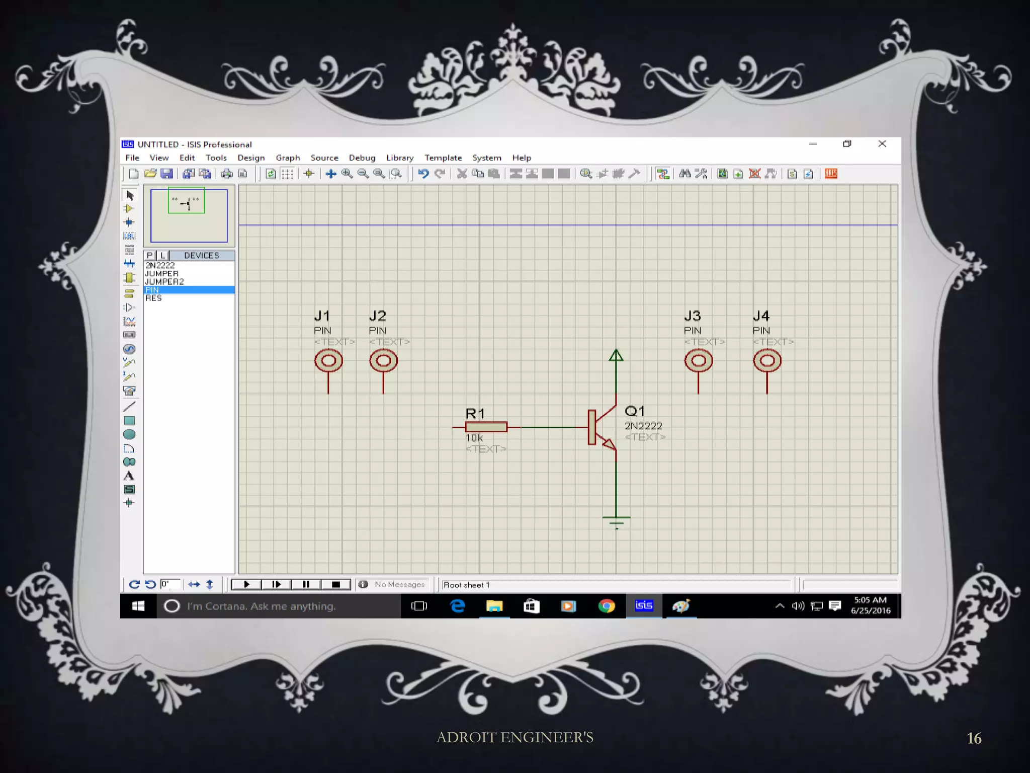
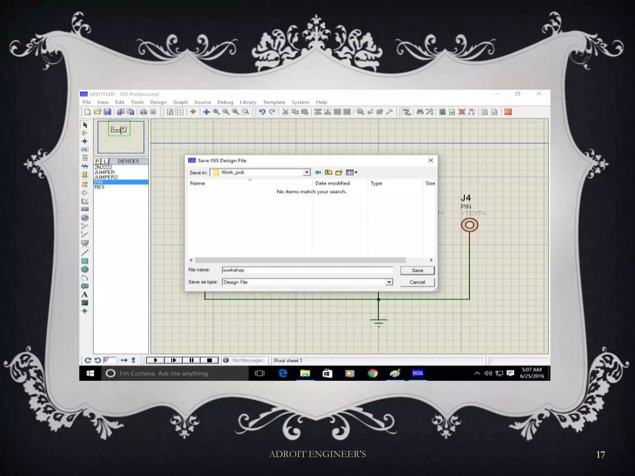
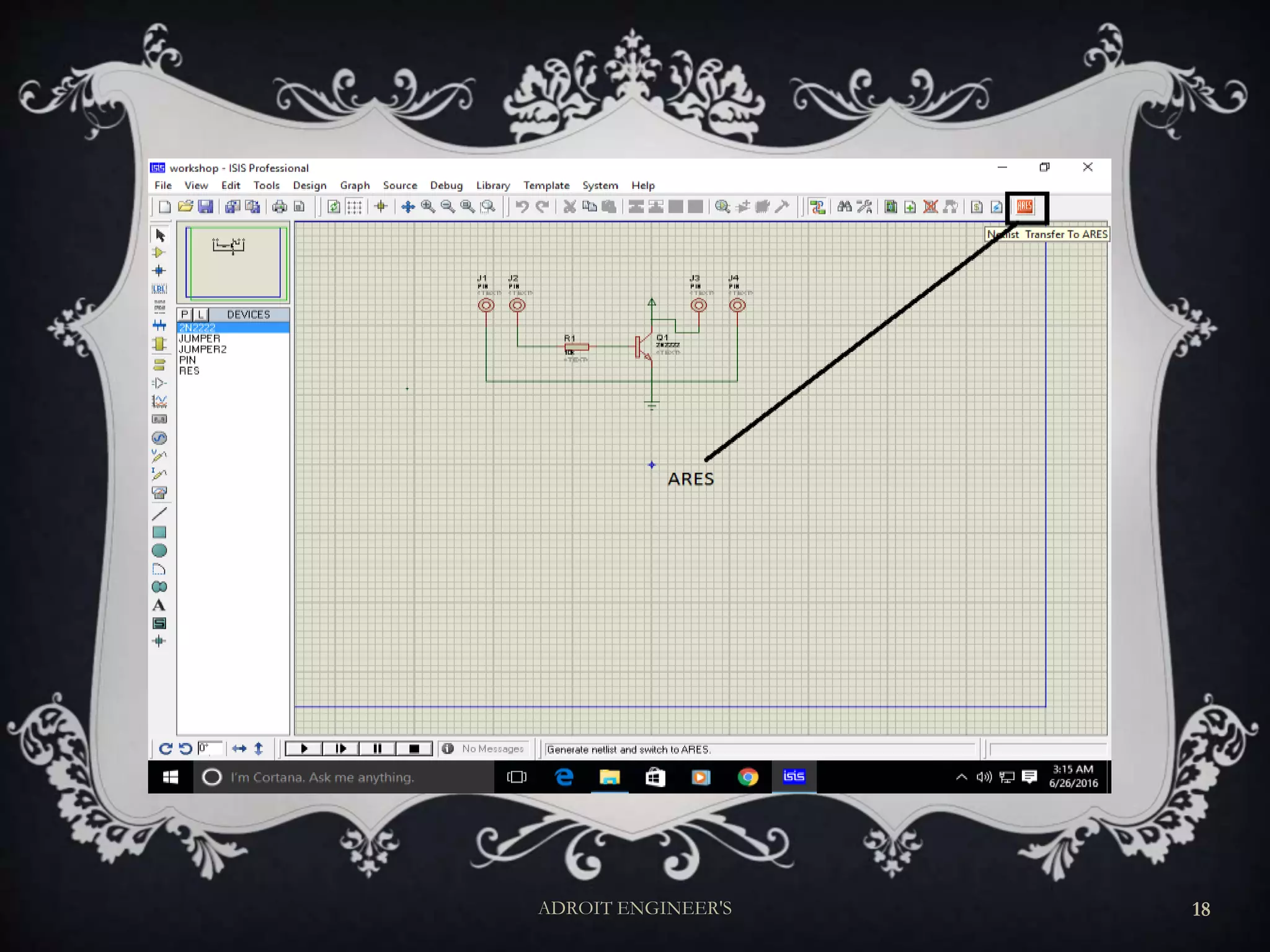
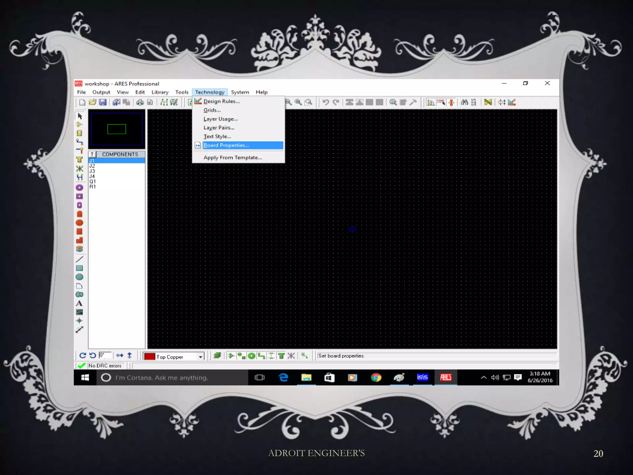
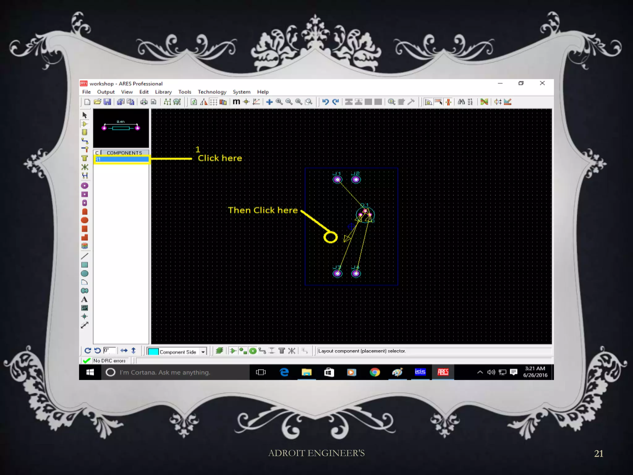
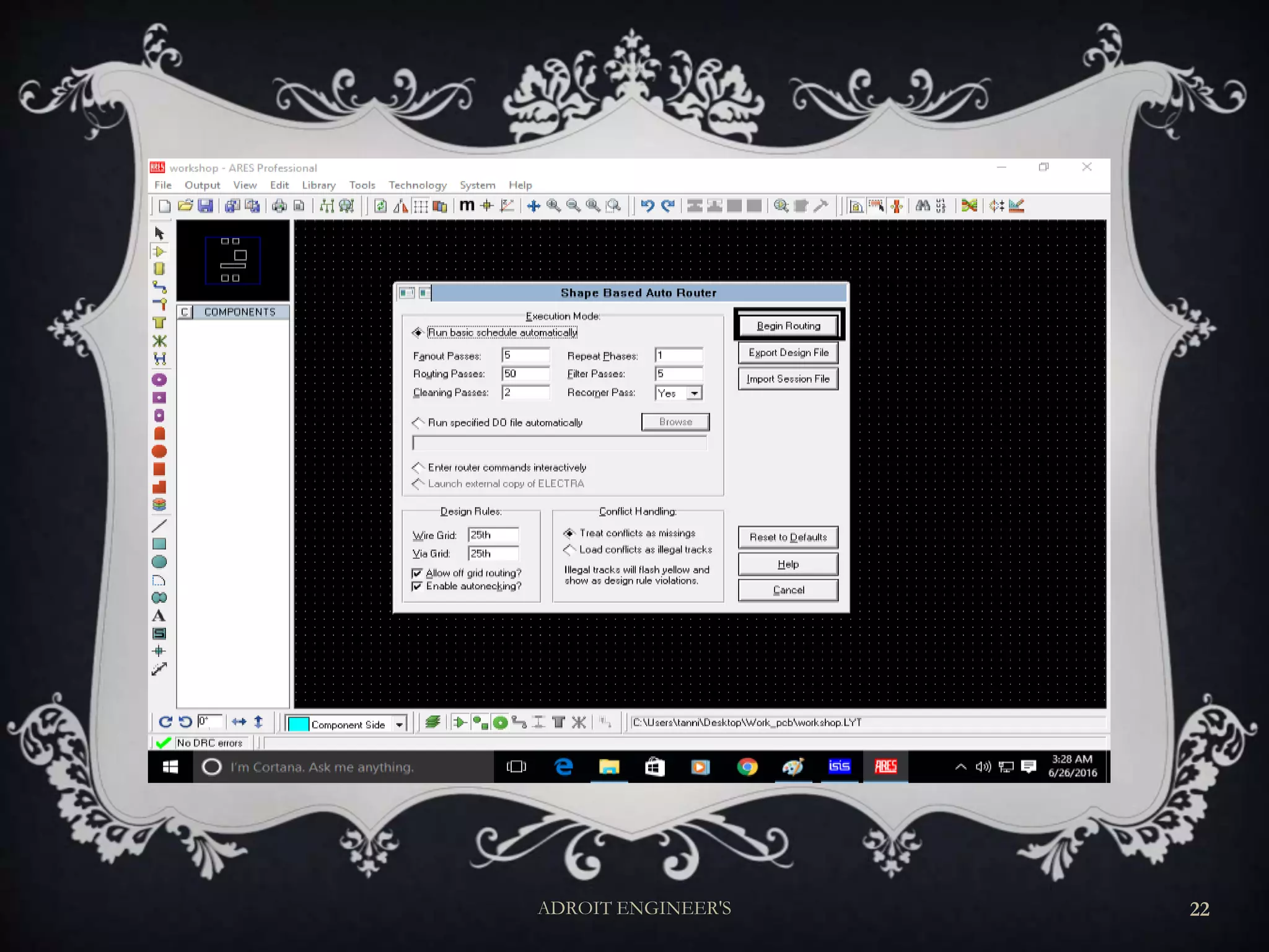
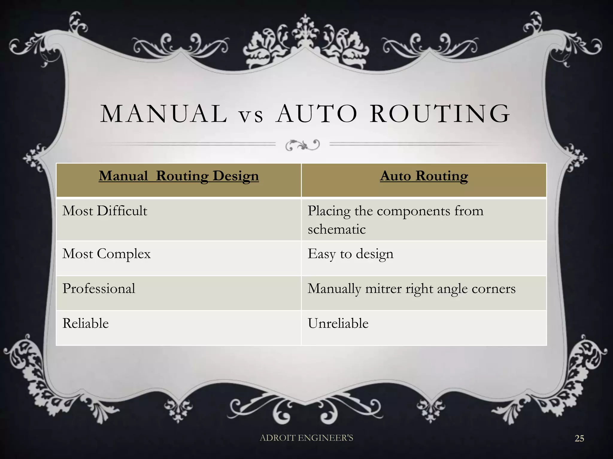
WORKSHOP ON PRINTED CIRCUIT
BOARD (PCB):
CAD DESIGNING AND FABRICATION
BASIC
Prepared and Presented by:
Engr. Mahmudur Rahman Rana Engr. Nasim Ahmed Khan
Director Director
Adroit Engineer’s Adroit Engineer’s
ADROIT ENGINEER'S 1
PRINTED CIRCUIT BOARD
(PCB)
A printed circuit board (PCB): Mechanically supports
and electrically connects electronic components using
conductive tracks, pads and other features etched from
copper sheets laminated onto a non-conductive substrate.
It can be: (1) Single Layer
(2) Double layer
(3) Multi layer
 PCB + Electronic component = Printed Circuit Assembly (PCA)
ADROIT ENGINEER'S 2
AUTO-ROUTING
Routing: is a step in the design of printed circuit
boards (PCBs) and integrated circuits (ICs).
Auto- Routing: is an automated design where the
components are routed automatically
after placing the components .
ADROIT ENGINEER'S 3
ISIS AND ARES
(AUTO ROUTING)
ADROIT ENGINEER'S 4
ADROIT ENGINEER'S 5
ADROIT ENGINEER'S 6
ADROIT ENGINEER'S 7
ADROIT ENGINEER'S 8
ADROIT ENGINEER'S 9
ADROIT ENGINEER'S 10
ADROIT ENGINEER'S 11
ADROIT ENGINEER'S 12
ADROIT ENGINEER'S 13
ADROIT ENGINEER'S 14
ADROIT ENGINEER'S 15
ADROIT ENGINEER'S 16
ADROIT ENGINEER'S 17
ADROIT ENGINEER'S 18
ADROIT ENGINEER'S 19
ADROIT ENGINEER'S 20
ADROIT ENGINEER'S 21
ADROIT ENGINEER'S 22
ADROIT ENGINEER'S 23
BASIC RULES OF PCB DESIGN
 Keep Tracks as short as possible
 Tracks should only have angles of 45 degrees.
 “Snake” your tracks around the board,
 Always take your track to the center of the pad
 Use a single track, not multiple tracks
 Make sure your tracks go right through the exact center of pads and components
 make your power tracks as BIG as possible.
 Keep things symmetrical
 Don’t leave any unconnected copper fills
ADROIT ENGINEER'S 24
MANUAL vs AUTO ROUTING
Manual Routing Design Auto Routing
Most Difficult Placing the components from
schematic
Most Complex Easy to design
Professional Manually mitrer right angle corners
Reliable Unreliable
ADROIT ENGINEER'S 25
MANUALLY PCB DESIGN
For PCB : “You must have……”
Software
Simulation of design
Datasheets of component used
Clear Concept about the Circuit
ADROIT ENGINEER'S 26
TO DESIGN A PCB
Copper Board:
(1) Component Side
(2) Layer/ Copper Side
ADROIT ENGINEER'S 27
DESIGN PARAMETERS
 Tracks
 Drills
(1) Drill Hole
(2) Drill Solder mark
 Green Coating and Heat Coating
 Component Package
 Clearance
ADROIT ENGINEER'S 28
TRACK
According to IPC-2221 Formula
 1A ; 0.03mm thickness, 0.35 mm trace width , 0.0427 ohm,
Vdrop 0.0427 V
 1 th (thou/mil) = 0.001 inch = 0.0254 mm
ADROIT ENGINEER'S 29
CLEARANCE
 IPC 2221B
Voltage Spacing
1 to 30 V 0.1 mm
31 to 150 V 0.6 mm
151 to 300 V 1.25 mm
301 to 500 V 2.50 mm
ADROIT ENGINEER'S 30
FABRICATION
Fabrication: is the action or process of manufacturing or
inventing something.
(1) Hand made/ Home made
(2) Industrial
(i) Small Factory (Manually)
(ii) Large Industry (Automation)
ADROIT ENGINEER'S 31
HAND OR HOME MADE
Components:
(i) Copper Clad
(ii) Iron
(iii)Inkjet Paper
(iv)Hand Drill
(v) Ferric Chloride
ADROIT ENGINEER'S 32
SMALL FACTORY
Screen Print
(1) Mash frame
(2) Photo-effective
(3) Ferric Chloride
(4) UV Exposer
(5) Print on a copper Clad
ADROIT ENGINEER'S 33
ANY QUESTIONS!!
BEST WISHES TO ALL
THANKS
TO EVERYONE
34ADROIT ENGINEER'S

Workshop on pcb