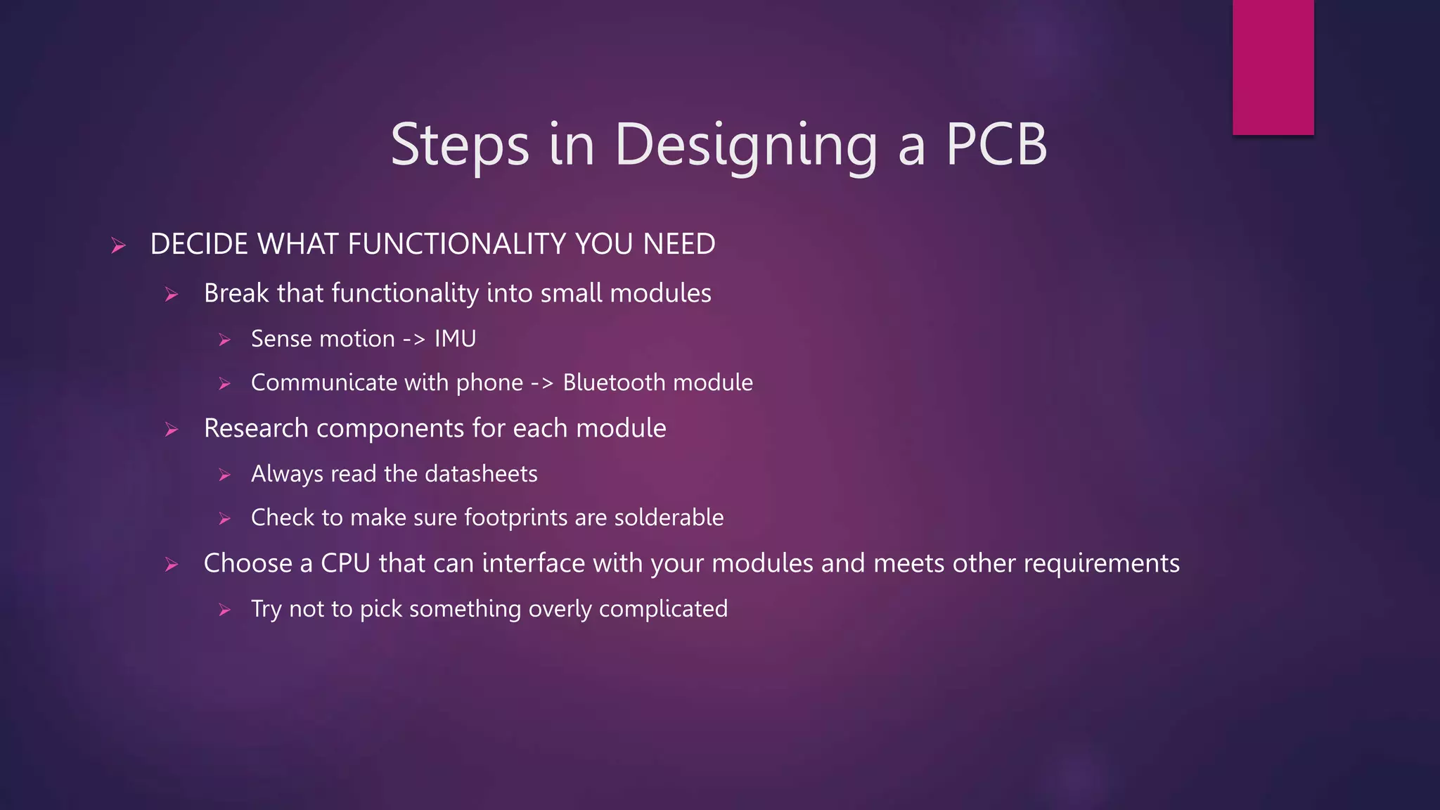
This document provides instructions for designing a printed circuit board (PCB) using Altium software. It describes the key steps which include:
1) Deciding on the functionality needed and choosing components to implement those functions
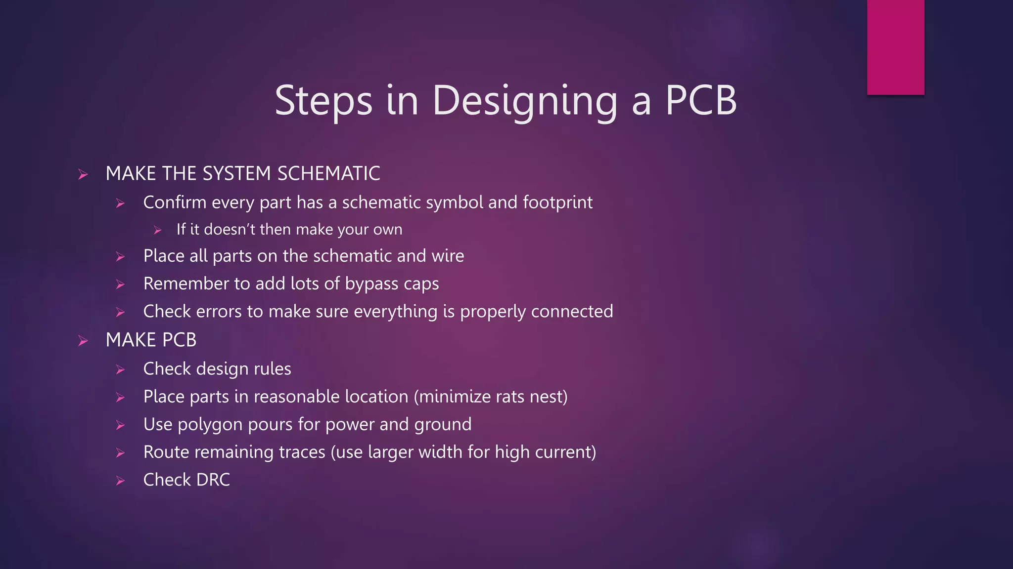
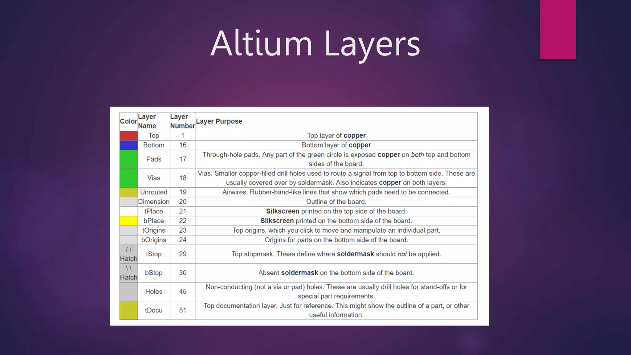
2) Creating a system schematic by placing components and wiring them together
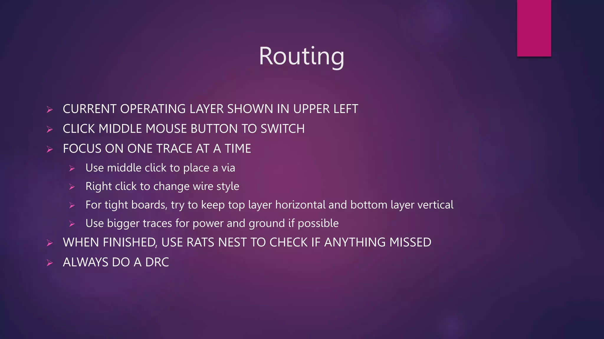
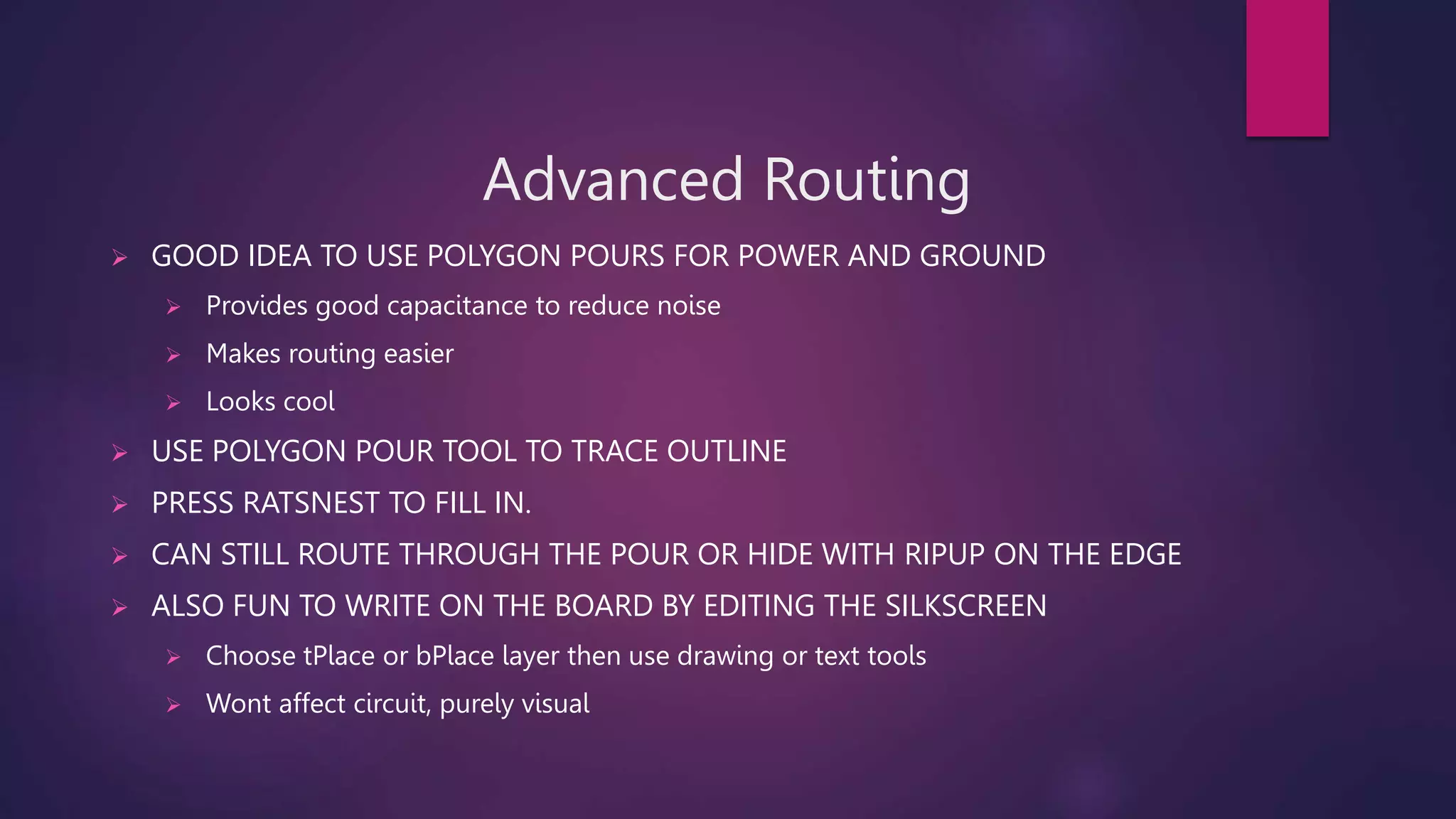
3) Designing the PCB layout by placing components, routing traces between them, and using techniques like polygon pours