This document provides an overview of PCB designing basics and tools. It defines a PCB as a printed circuit board that physically supports and wires surface-mounted and through-hole components using a FR-4 panel with copper foil laminated on one or both sides. The basic steps in PCB design are: 1) schematic capture, 2) component placement, and 3) routing and exporting output files in Gerber or ODB format. Popular PCB design tools mentioned include Cadence Allegro, Mentor Graphics PADS, Altium PCB Designer, and Eagle PCB Design.
In this document
Powered by AI
This section introduces PCB design, its basics, and the essential tools used in the process.
Describes what a printed circuit board (PCB) is, its composition, including the FR-4 panel and copper foil.
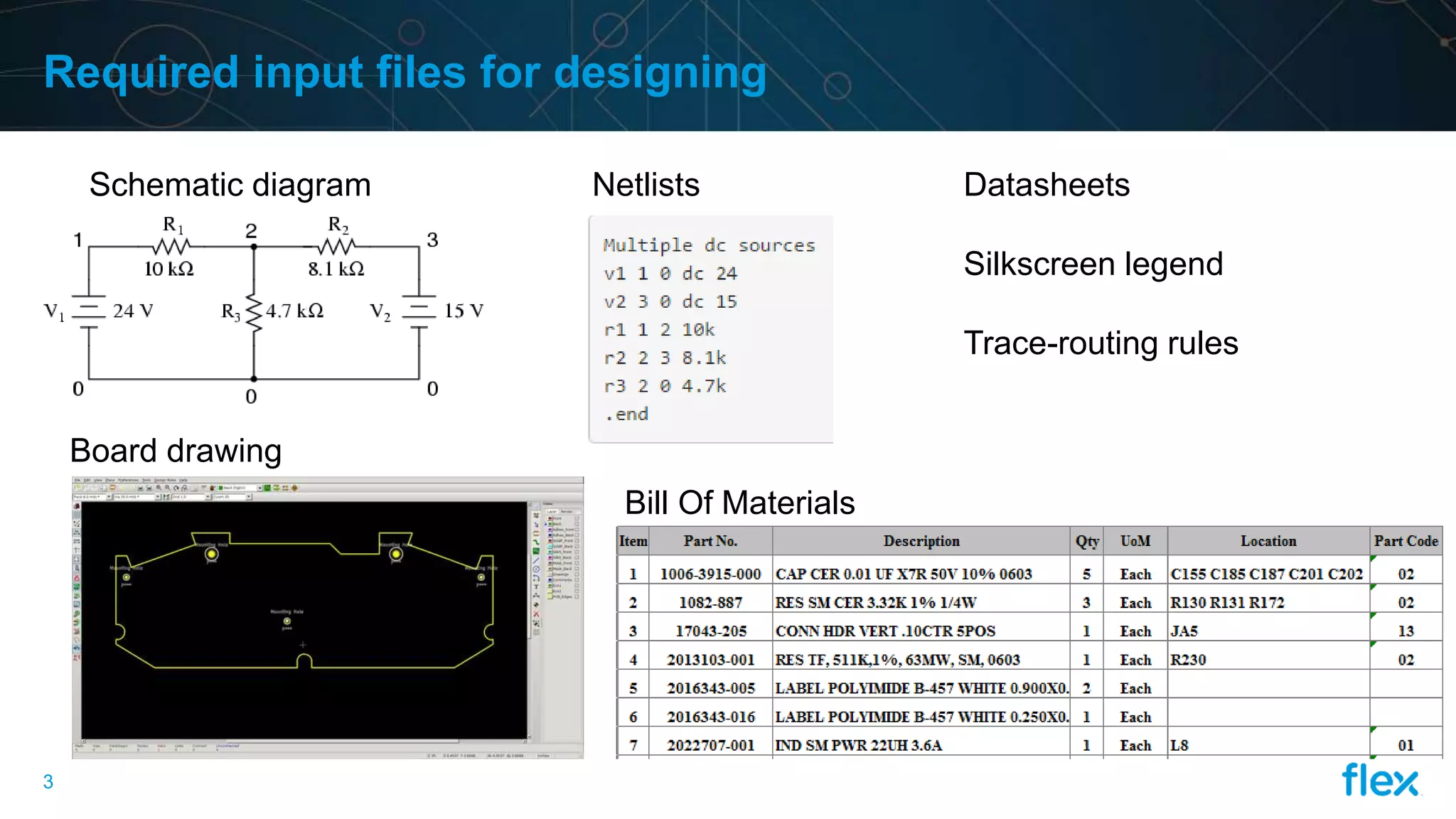
Lists essential input files needed for PCB design, such as schematic diagrams and Bill of Materials.
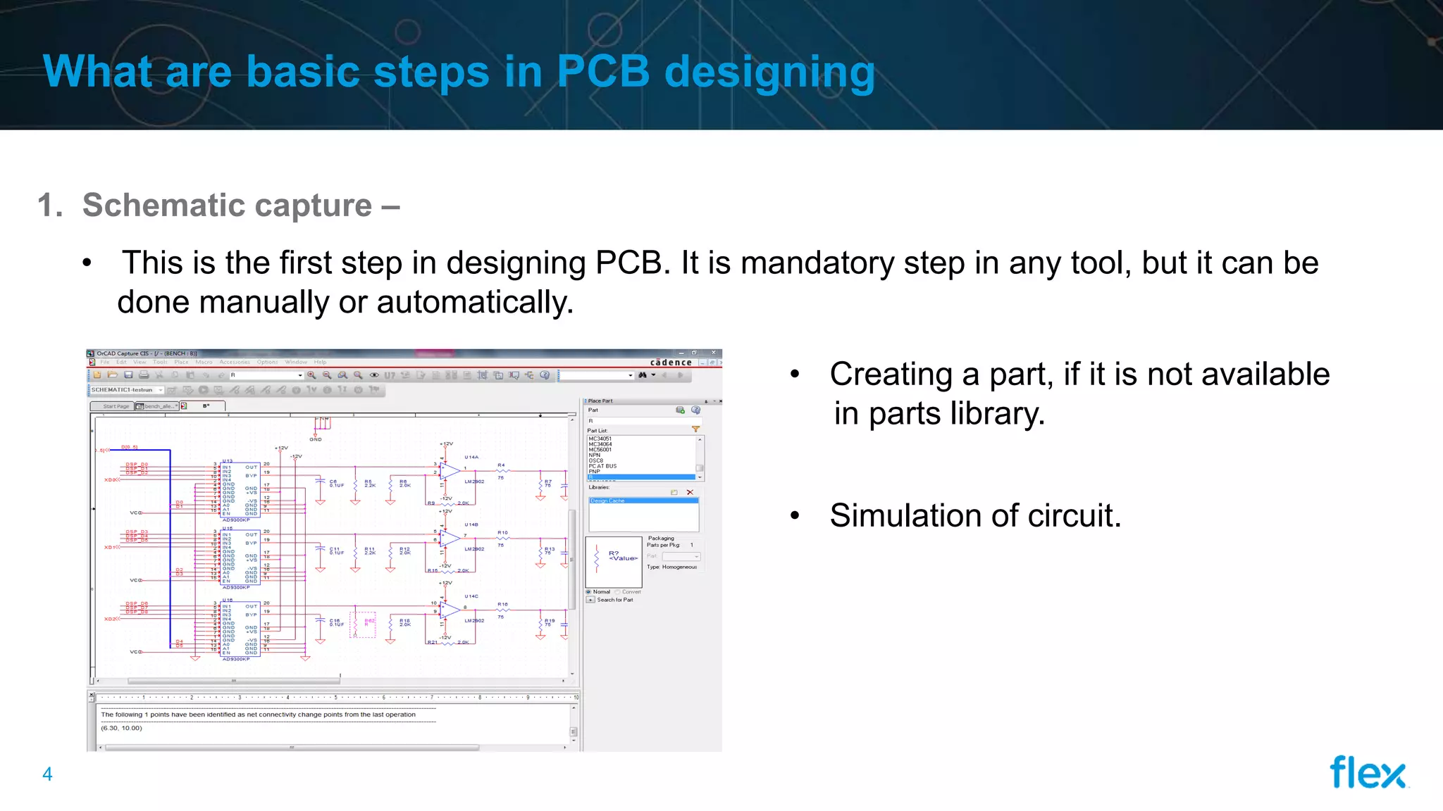
Covers the first step in PCB design, focusing on schematic capture, part creation, and circuit simulation.
Details the process of component placement, including decal assignment and arranging parts by functionality.
Explains the routing process, design rules, and the export of output files in different formats.
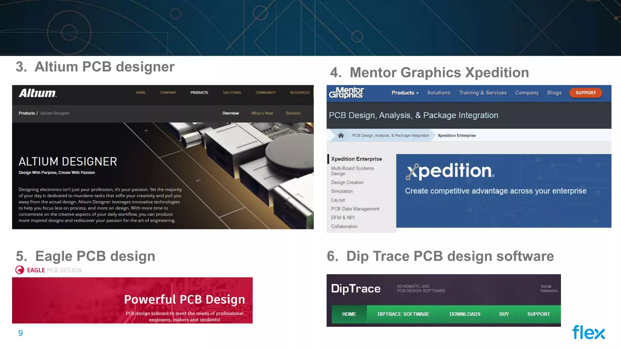
Lists various PCB design tools such as Cadence Allegro, Mentor Graphics PADS, and Altium.
Provides thank you notes and references used for the presentation.
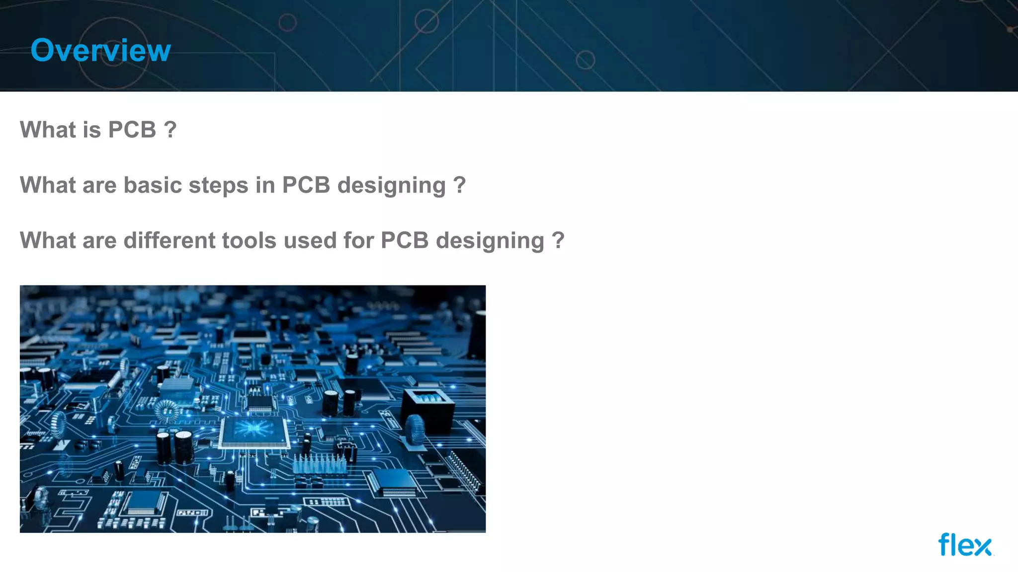
Overview
What is PCB?
What are basic steps in PCB designing ?
What are different tools used for PCB designing ?
3.
2
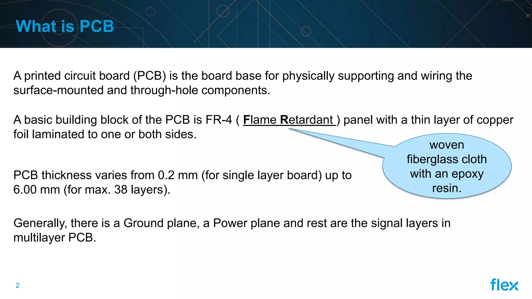
What is PCB
Aprinted circuit board (PCB) is the board base for physically supporting and wiring the
surface-mounted and through-hole components.
woven
fiberglass cloth
with an epoxy
resin.
A basic building block of the PCB is FR-4 ( Flame Retardant ) panel with a thin layer of copper
foil laminated to one or both sides.
PCB thickness varies from 0.2 mm (for single layer board) up to
6.00 mm (for max. 38 layers).
Generally, there is a Ground plane, a Power plane and rest are the signal layers in
multilayer PCB.
4.
3
Required input filesfor designing
Schematic diagram Netlists
Board drawing
Bill Of Materials
Datasheets
Silkscreen legend
Trace-routing rules
5.
4
What are basicsteps in PCB designing
1. Schematic capture –
• This is the first step in designing PCB. It is mandatory step in any tool, but it can be
done manually or automatically.
• Creating a part, if it is not available
in parts library.
• Simulation of circuit.
6.
5
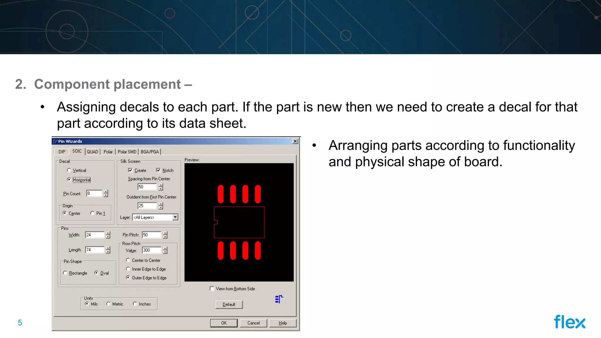
2. Component placement–
• Assigning decals to each part. If the part is new then we need to create a decal for that
part according to its data sheet.
• Arranging parts according to functionality
and physical shape of board.
7.
6
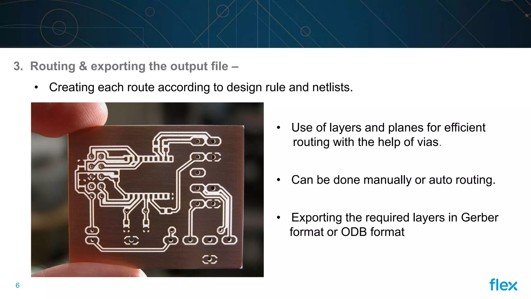
3. Routing &exporting the output file –
• Creating each route according to design rule and netlists.
• Use of layers and planes for efficient
routing with the help of vias.
• Can be done manually or auto routing.
• Exporting the required layers in Gerber
format or ODB format
8.
7
What are thedifferent PCB designing tools
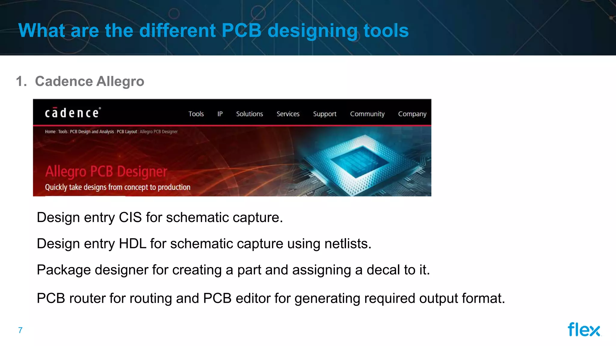
1. Cadence Allegro
Design entry CIS for schematic capture.
Design entry HDL for schematic capture using netlists.
Package designer for creating a part and assigning a decal to it.
PCB router for routing and PCB editor for generating required output format.
9.
8
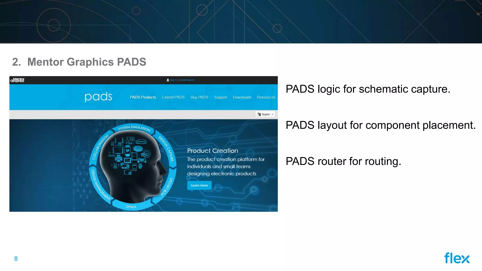
2. Mentor GraphicsPADS
PADS logic for schematic capture.
PADS layout for component placement.
PADS router for routing.