Downloaded 170 times


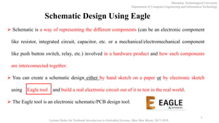
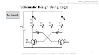
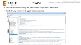


The document serves as a lecture outline for an embedded systems course, focusing on topics such as embedded hardware design, electronic components, and PCB design using EDA tools like Eagle and Orcad. It presents step-by-step tutorials for creating schematics and PCB layouts, along with discussions on integrated circuits and design principles. Students are also assigned homework related to EDA tools, schematics, PCB design guidelines, and fabrication techniques.