Downloaded 293 times
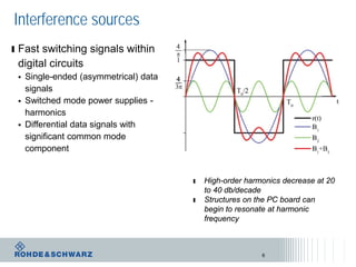
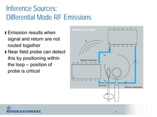
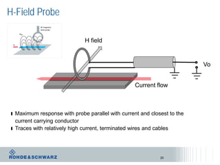
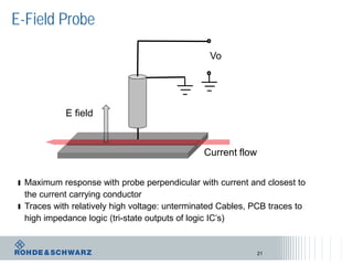
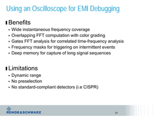
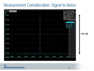
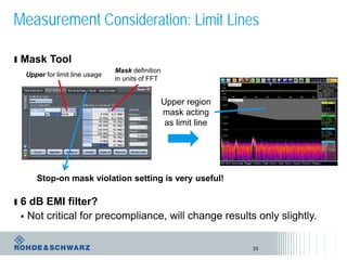
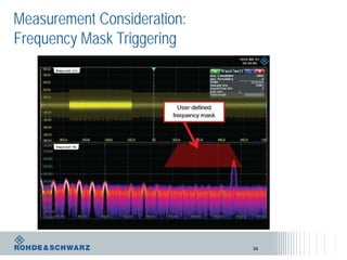
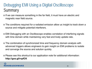

This document discusses debugging electromagnetic interference (EMI) using digital oscilloscopes, detailing key concepts such as radiated emissions, interference sources, and coupling mechanisms. It outlines practical steps to reduce differential and common mode RF emissions, explores the use of near-field probes for analysis, and emphasizes the importance of both time and frequency domain measurements in EMI debugging. The document concludes that synchronizing time and frequency analysis can help engineers quickly identify and mitigate EMI issues.


![Getting Started with Apache Spark: Big Data Made Simple [Free Meetup]](https://cdn.slidesharecdn.com/ss_thumbnails/apachesparkgettingstarted-260203175547-8361bcc3-thumbnail.jpg?width=640&height=640&fit=bounds)


