Downloaded 132 times


![28
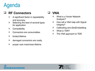
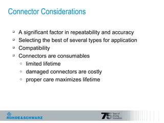
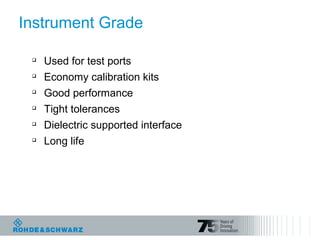
Why use Vector Network Analysis?
Very low level signals can be measured more accurately with
narrow bandwidths
Can measure very fast Rise Times
The 4-port, single-ended S parameters have become a de-facto
standard for describing the electrical properties of any 4-port
interconnect.
ı For example, IEEE P802.3ap Task Force uses measured S-parameters as test cases
[9] for proposed solutions to the problem of 10 Gbit/s Ethernet over backplanes.
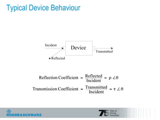
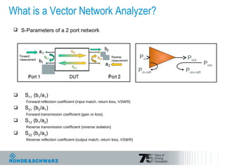
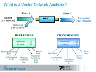
What are the numbers in S..
o the first index being the going out port
o the second index is the coming in port.
o Example: Gain or Loss of Device is S21](https://image.slidesharecdn.com/17ad722e-20ef-4c8b-ab9a-766a8d562210-150207005816-conversion-gate02/85/Design-Con-VNA-28-320.jpg)

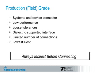
![Reslution and Resolution Enhancement Factor
0,00E+00
5,00E-02
1,00E-01
1,50E-01
2,00E-01
2,50E-01
3,00E-01
3,50E-01
-2,00E-09 0,00E+00 2,00E-09 4,00E-09 6,00E-09 8,00E-09 1,00E-08 1,20E-08
time [ns]
ReflectionFactor[U]
ZVA: 1 GHz - 20 GHz ZNB: 1 GHz - 8 GHz REF: 2.5
ZVA: Start: 10 MHz - 20 GHz
ZNB: Start 10 MHz - 8 GHz, REF: 2.5
fstep: 10 MHz](https://image.slidesharecdn.com/17ad722e-20ef-4c8b-ab9a-766a8d562210-150207005816-conversion-gate02/85/Design-Con-VNA-55-320.jpg)

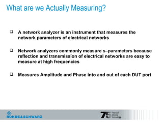
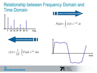
This document discusses using a vector network analyzer (VNA) for signal integrity testing. It begins with an overview of RF connectors and their impact on measurement accuracy. It then describes how a VNA works, measuring both amplitude and phase to determine S-parameters. Key aspects covered include calibration to define a reference plane, measuring transmission and reflection parameters, and converting frequency domain data to the time domain. Applications discussed include time domain reflectometry for fault detection and measuring rise times.


![RF Module Design - [Chapter 5] Low Noise Amplifier](https://cdn.slidesharecdn.com/ss_thumbnails/rfch5-150613070346-lva1-app6891-thumbnail.jpg?width=640&height=640&fit=bounds)


![RF Module Design - [Chapter 1] From Basics to RF Transceivers](https://cdn.slidesharecdn.com/ss_thumbnails/rfch1-150613070344-lva1-app6892-thumbnail.jpg?width=640&height=640&fit=bounds)