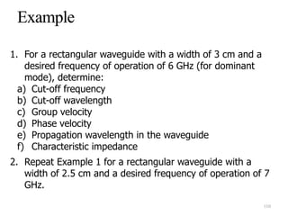
Downloaded 316 times
![Directional Coupler Parameter
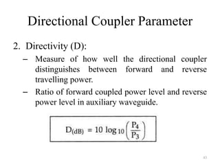
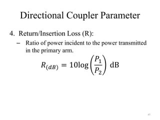
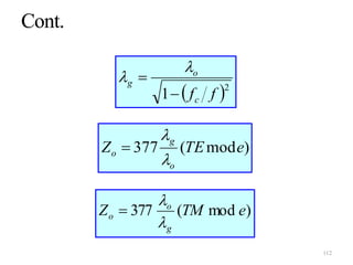
3. Isolation (I):
– Measures the directional properties.
– Ratio of incident power in main waveguide to the
reverse power at auxiliary waveguide.
– I = C.D
– I (dB)= [C]dB+[D]dB
44](https://image.slidesharecdn.com/rfandmicrowavecomponentsanddevices-171005145621/85/Rf-and-microwave-components-and-devices-44-320.jpg)
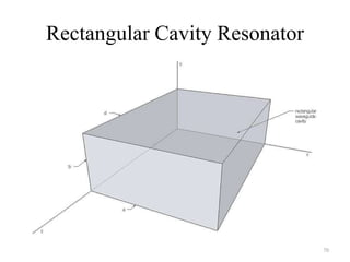
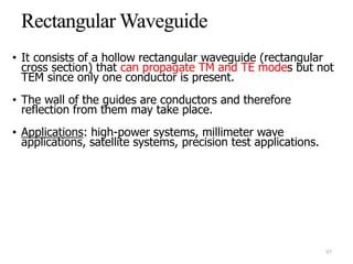
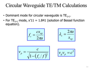
![• It is a standard convention to have the longest side of the
waveguide along x-axis [a (width) > b (length)]
98](https://image.slidesharecdn.com/rfandmicrowavecomponentsanddevices-171005145621/85/Rf-and-microwave-components-and-devices-98-320.jpg)

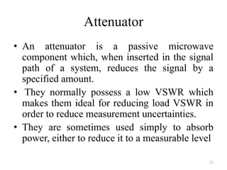
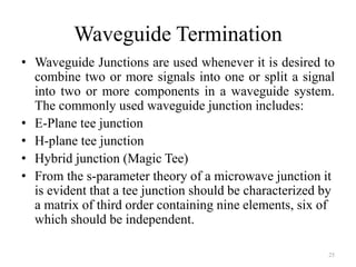
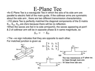
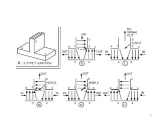
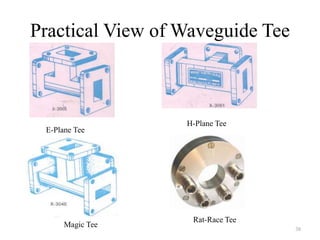
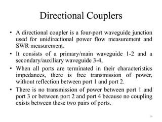
Chapter 4 discusses various RF/MW components and devices, focusing on coupling mechanisms in waveguides such as probes, loops, and apertures, highlighting their principles of operation and efficiency factors. It also explores impedance matching methods, including the use of windows, posts, and screws, as well as waveguide junctions like E-plane and H-plane tees and hybrid tees for signal manipulation. Additionally, the chapter covers directional couplers, detailing their performance parameters, including coupling factor, directivity, isolation, and return loss.