SlideShare a Scribd company logo
1 of 80
Download to read offline
True Differential Measurements


Characterization of Balanced Devices and Channels
Dr. Chris Scholz
Product Manager, Vector Network Analyzers                              Reflectometer 2

Christopher.scholz@rsa.rohde-schwarz.com                   Meas. Receiver
                                                           Ref. Receiver                 PORT 2
(817) 422 2512
                                                                       Reflectometer 4
                                                           Meas. Receiver
                                                           Ref. Receiver                 PORT 4
                                                                                                      Logical
                                               Error                                                  PORT 2
                                              corrected               Reflectometer 1
                                             Mag Phase     Meas. Receiver                         Balanced
                                              detection                                            DUT
                                             and control   Ref. Receiver                 PORT 1
                                             by software
                                                                                                      Logical
                                                                                                      PORT 1
                                                                       Reflectometer 3
                                                           Meas. Receiver
                                                           Ref. Receiver                 PORT 3
Outline
                                                                                             Reflectometer 2
                                                                                Meas. Receiver
                                                                                Ref. Receiver                  PORT 2


                                                                                             Reflectometer 4
                                                                               Meas. Receiver
                                                                                Ref. Receiver

ı Introduction to Signal Integrity
                                                                                                               PORT 4
                                                                                                                                  Logical
                                           Error                                                                                  PORT 2
                                          corrected                                          Reflectometer 1
                                         Mag Phase                                                                        Balanced
   Timing                                detection                            Meas. Receiver
                                                                                                                           DUT
                                         and control                            Ref. Receiver
   Signal Quality
                                                                                                               PORT 1
                                         by software
                                                                                                                                  Logical

ı Balanced Architectures                                                                     Reflectometer 3
                                                                                                                                  PORT 1
                                                                               Meas. Receiver

   The need for balanced architectures
                                                                                Ref. Receiver                  PORT 3


   Ideal vs. non-ideal devices
ı Measurement Techniques for Balanced Architectures
   Single mode vs. Differential Mode
   Mixed mode S-Parameters                 Trc18 Sdd21 dB Mag 0.5 dB / Ref -23 dB Ch1 Cal int
                                            Trc21 Sdd21 dB Mag 0.5 dB / Ref -23 dB Ch2 Cal int
                                                                                                                        2 of 16 (Max)


   TureDifferential vs. Virtual Differential
                                              Sdd21
                                             -20.0


   TruDifferential Vector Network Analyzer  -20.5


ı Experimental Examples
                                             -21.0


                                             -21.5


                                             -22.0


                                             -22.5


                                             -23.0


                                             -23.5


                                             -24.0


                                            Ch1      Start -25 dBm —            Freq 1 GHz                              Stop 0 dBm
                       1/29/2013            Ch2      Start -28 dBm —               2
                                                                                Freq 1 GHz                              Stop -3 dBm
                                           3/8/2007, 1:10 PM
Introduction – Signal Integrity

ı What is Signal Integrity?
    Signal integrity or SI is a set of measures of the quality of an electrical signal.
    If the PCB or package already exists, the designer can also measure the
     impairment presented by the connection using high speed instrumentation
     such as a vector network analyzer. For example, IEEE P802.3ap Task Force
     uses measured S-parameters as test cases[9] for proposed solutions to the
     problem of 10 Gbit/s Ethernet over backplanes.
      (Source: Wikipedia, last accessed 01/29/2013)


ı Two Key Aspects of SI:

               Timing                Signal Quality


                         1/29/2013                                   3
Introduction – Signal Integrity

ı Timing

    Jitter
      RJ, DJ, SJ, PJ, DDJ, DCD, ISI, etc.
    interconnect flight time vs bit period
    chip-to-chip vs on-chip
    packaging


                       1/29/2013              4
Introduction - Signal Integrity

ı Signal Quality
                                                  Noise = (S+N)-S
    Ringing
                                             10
    Cross talk                              8

    Distortion                              6

    Ground Bounce                           4


                                 amplitude
    Ground Noise                            2


    Signal Loss                             0


    Power Supply Noise                      -2

                                             -4

                                             -6
                                                           time


                     1/29/2013                                      5
Introduction – Signal Integrity

ı Reflection Noise
    Caused by impedance mismatch, vias, interconnect discontinuities

ı Crosstalk Noise
    Caused by electromagnetic coupling between traces and vias

ı Power and Ground Noise
    Caused switching noise of the power and ground delivery systems

ı EMC/EMI Susceptibility


                      1/29/2013                               6
Balanced Architectures


             1/29/2013   7
Differential Signaling

Unbalanced Device/Channel                 Balanced (differential) Device/Channel


                                                                     c
                                                a

                                      2
    1                                      1                                  2
                                                b
                                                                     d

•       Signals referring to ground       ı Signals with equal amplitude but 180° phase
                                            shift
                                          • Also supports a common-mode (in-phase)
                                            signal
                                          • Virtual ground
Balanced devices - Why balanced design?
                                                   ı Advantages:
                                                   ı High noise immunity
                                                         Minimizes Power and
                                                          ground plane noise
                                                         Minimizes EMI
                                                          susceptibility
                                                         Minimizes Cross talk
Components with
balanced design:                                   ı    Low radiated noise
                                                   ı    High integration density
•   Amplifiers                                     ı    Lower power
•   Mixers
                                                        consumption
•   Filters (e.g. SAW filters)
•   PCB layout in mobile phones
•   LAN adapters, converters, filters
•   PC components (HDD control, etc)
•   Almost all signals high-speed serial data signals
Ideal Balanced Device Characteristics
                                         Gain = 1

     Differential-mode signal

                                                               Fully balanced
     Common-mode signal
     (EMI or ground noise)

                                         Gain = 1

     Differential-mode signal                                   Balanced to
                                                                single ended
     Common-mode signal
     (EMI or ground noise)


Ideally, balanced devices transmit differential and reject common-mode signals


                        1/29/2013                                    10
Non-Ideal Balanced Device Characteristics
                                                 Differential to common-
ı Non-ideal balanced devices convert modes       mode conversion


                                             +
                                                        Generates EMI


                                                    Susceptible to EMI

                                                 Common-mode to
                                                 differential conversion


                    1/29/2013                          11
Non-Ideal Balanced Device Characteristics

ı Non-ideal balanced devices convert input modes


                                                   Differential to common-
                                                   mode conversion


                                                   Common-mode to
                                                   differential conversion


                    1/29/2013                                12
Measurement Techniques for Balanced
Devices


            1/29/2013                 13
Parameters to Test for a Balanced Device

ı   Performance in pure differential mode
ı   Performance in pure common mode
ı   Conversion from differential mode to common mode (in both directions)
ı   Conversion from common mode to differential mode (in both directions)


                       1/29/2013                              14
Balanced Devices Characteristics

ı Real Devices
    Propagation of both common mode and differential mode signals
    Mode conversion due to non-symmetric design
    Susceptability of noise (mainly common mode)

    Detailed insight of differential/common mode response required

ı Description of balanced devices via special type of S-Parameters:
    Mixed-Mode S-Parameters


                       1/29/2013                              15
Challenge when measuring balanced devices

ı   Network analyzers are unbalanced
ı   Classic Network Analyzers are 2-port instruments
ı   No balanced calibration standards
ı   No standard reference impedance (Z0) for balanced device
ı   Characterization of common and differential transmission model


                       1/29/2013                              16
Measurement with Physical BalUns

                            Measurement with differential mode
                            signals at a balanced device
       Unbalanced
       network analyzer


                     DUT


                    Balun


                1/29/2013                   17
Measurement with Physical Transformers

                                    Measurement with common
           Unbalanced               mode signals at a balanced
           network analyzer         device


                              DUT


             1/29/2013                     18
Balanced Device Characteristics
Balun setup for Mixed-Mode-Characterization


  bal                           DUT                           bal


unbal                                                         unbal


 Each 2-port combination between balanced and unbalanced ports is
 necessary for complete mixed mode characterization.
Balanced Device Characteristics
Physical BalUns: Disadvantages
ı Calibration plane different from desired measurement plane
ı Degradation of measurement accuracy due to poor RF performance
ı Different configurations for different modes necessary (e.g. differential to
  common-mode conversion)
ı Limited in frequency range

ı Solution:
    Us ideal (virtual) transformer to characterize mixed mode S-parameters of the
     DUT using virtual, ideal transformers

Modal Decomposition Method
Use True Differential Method


                       1/29/2013                                 20
Basic Architecture: Definition of Differential
Measuremets
Measurement Principle

ı VirDi = Virtual differential Mode
   Characterization of balanced DUT as single ended DUT with mathematical
    calculation of mixed-mode S-Parameters form single ended S-Parameters
ı TruDi = True differential Mode
   Stimulation of DUT with true differential and common mode signals with
    calculation of mixed-mode S-Parameters from error corrected mixed mode
    wave quantities


                       1/29/2013                           21
Virtual Differential Measurement


ı Subsequent single ended measurements with post processing using linear
  superposition
ı Applicable for all passive devices and active devices operating in their linear
  region
ı Large deviations compared to TruDi in large signal operation, especially in
  terms of compression curve characteristics
   Nonlinear behavior of the DUT forbids linear superposition


                       1/29/2013                                22
True Differential Measurement


ı The DUT is stimulated using a real differential mode or real common mode
  signal
ı Better accuracy in small signal operation
ı Accurately measure compression under large signal operation


                     1/29/2013                              23
ZVA – True Differential Mode

ı Coherent sources
   Generation of true differential and common mode stimulus signals
   At least one signal output can be adjusted in amplitude and phase with
    respect to the other
ı Simultaneous measurement of two reference signals (a waves) and two
  measurement signals (b waves)
ı Four-port calibration in the reference plane
   Vector-corrected measurement of a single ended waves or voltages (a and b
    waves)
ı Calculation of true differential S-Parameters from vector corrected wave
  quantities


                     1/29/2013                             24
A True Differential Network Analyzer

                                               Reflectometer 2

                              Meas. Receiver

                              Ref. Receiver                      PORT 2


                                               Reflectometer 4

                              Meas. Receiver

                              Ref. Receiver                      PORT 4
                                                                                     Logical
                                                                                     PORT 2
              Error
            corrected
                                               Reflectometer 1
           Mag Phase                                                           Balanced
                              Meas. Receiver
            detection                                                            DUT
           and control        Ref. Receiver
                                                                 PORT 1
           by software
                                                                                     Logical
                                                                                     PORT 1
                                               Reflectometer 3

                              Meas. Receiver

                              Ref. Receiver                      PORT 3


                  1/29/2013                                               25
True Differential Measurements with R&S Network
Analyzers ZVA and ZVT


             1/29/2013               26
Sweep modes (R&S®ZVA-K6)
            differential mode 180°                  common mode 0°


Coherent signals of arbitrary phase and amplitude imbalance are possible
   Sweep Modes:
     Frequency
     Phase (Phase of the stimulating signal can be swept from 0° to 180° )
     Magnitude (Variation of the relative magnitude of the differential signals)
     “Classical” calibration techniques sufficient (full two port)
      Investigation of the DUT under real conditions


                       1/29/2013                                 27
Typical measurements quality parameters

ı   Differential and common mode insertion loss
ı   Differential and common mode return loss
ı   NEXT-Measurements (Near End Crosstalk)
ı   FEXT-Measurements (Far End Crosstalk)
ı   Amplitude-Imbalance
ı   Phase-Imbalance
ı   Common-Mode Rejection Ratio (CMRR)


                       1/29/2013                  28
True Differential vs. Virtual Differential
TruDi vs. VerDi


               1/29/2013                     29
Modal Decomposition Method Principle

 4-port device with                                       Description of virtual
 16 measured                                              ideal transformers
 unbalanced S-
 parameter


                                  Calculated mixed mode
                                  S-parameters


ı Calculation of the mixed mode S-parameters using unbalaced S-Parameters
 and virtual transformers


                      1/29/2013                             30
Modal Decomposition Method

                                  test fixture

   a      Port 1                                                          Port 3   a
                                     DUT
                                    DUT
   b                                                                               b
          Port 2                                                          Port 4


                a 1   S 11      S   12   S    13   S   14
                                                                  b 4
                                                                   
                a 2   S 2 1    S   22   S    23   S   24 
                                                                  b 3
                a  S            S        S         S           b 
                3   31              32        33       34
                                                                   2
                a 4  S 4 1
                                S   42   S    43   S   44 
                                                                   b 1
                                                                       
ı Measure the balanced 2-port device as unbalanced 4-port device with
 unbalanced VNA


                     1/29/2013                                       31
Solution: Modal Decomposition Method


                                    [Z]


                                 [P], [Q]


                                [Zm]
ı Calculate the mixed mode Zm-parameters of the combination of DUT with
 transformers.


                    1/29/2013                             32
Port Configurations Mixed Mode DUT

ı Physical single ending ports  logical balanced ports


       Port 3   Port 1               Port 4      Port 2          physical ports


                         DUT                                     logical ports
            Port 1                      Port 2


ı Different impedances for common-mode and differential-mode
      differential-mode (ideally matched)  100           ( =2*Z0 )
      common-mode (ideally matched)        25           ( = 1/2*Z0 )


                         1/29/2013                                       33
Modal Decomposition Method
Mixed Mode S-Parameter Matrix

             DU                                    Differential-Mode
                                                   stimulus
                                                                            Common-Mode
                                                                            stimulus
              T                                    Port 1       Port 2      Port 1   Port 2
Logical Port 1    Logical Port 2


                 Differential-     Port 1          S dd11      S d d1 2   S dc11    S dc12 
                 mode
                                   Port 2
                                                  S            S dd 22    S dc 21   S d c 22 
                 Response
                                                   dd 21                                     
                 Common-           Port 1          S cd11      S cd12     S cc1 1   S cc12 
                 mode
                                   Port 2                                                    
                 Response
                                                   S cd 21
                                                               S cd 22    S cc 21   S cc 22 
                 Naming Convention: S mode res., mode stim., port res., port stim.


                       1/29/2013                                           34
Mixed Mode S-Matrix: DD Quadrant

  input reflection               reverse transmission

                S dd    11      S dd   12      S dc   11   S dc   12 
                                                                     
                S dd    21      S dd   22      S dc   21   S dc   22 
                S cd   11       S cd   12      S cc   11   S cc   12
                                                                      
                                                                     
                S cd    21      S cd   22      S cc   21   S cc   22 
   forward transmission                      output reflection

ı Describes fundamental performance in pure differential-mode operation


                     1/29/2013                                35
Mixed Mode S-Matrix: CC Quadrant

                 input reflection                           reverse transmission

              S dd   11          S dd   12   S dc   11   S dc   12 
                                                                   
              S dd   21          S dd   22   S dc   21   S dc   22 
              S cd   11          S cd   12   S cc   11   S cc   12
                                                                    
                                                                   
              S cd
                     21          S cd   22   S cc   21   S cc   22 
                                                                    


                 forward transmission                     output reflection

ı Describes fundamental performance in pure common-mode operation


                      1/29/2013                                         36
Mixed Mode S-Matrix: DC Quadrant

                         input reflection                     reverse transmission

                 S dd    11         S dd   12   S dc   11   S dc   12 
                                                                      
                 S dd     21        S dd   22   S dc   21   S dc   22 
                 S cd    11         S cd   12   S cc   11   S cc   12
                                                                       
                                                                      
                 S cd
                         21         S cd   22   S cc   21   S cc   22 
                                                                       

                  forward transmission                              output reflection
ı Describes conversion of a common-mode stimulus to a differential-mode
  response
ı Terms are ideally equal to zero with perfect symmetry
ı Related to the generation to EMI

                         1/29/2013                                         37
Mixed Mode S-Matrix: CD Quadrant

   input reflection                reverse transmission
                     S dd    11   S dd   12   S dc   11   S dc   12 
                                                                    
                     S dd    21   S dd   22   S dc   21   S dc   22 
                     S cd    11   S cd   12   S cc   11   S cc   12
                                                                     
                                                                    
                     S cd
                             21   S cd   22   S cc   21   S cc   22 
                                                                     


    forward transmission                  output reflection

ı Describes conversion of a differential-mode stimulus to a common-mode
  response
ı Terms are ideally equal to zero with perfect symmetry
ı Related to the susceptibility of EMI

                      1/29/2013                                    38
3-Port device
single ended  common / differential-mode
          Single-ended                          differential-mode
                                                common-mode

   Port 1                                                               Port 2
   (unbalanced)                      DUT                                (balanced)

                                     Single     Diff.-     Com.-
                                     Ended      mode       mode
                                     Stim.      Stim.      Stim.

                                     Port 1   Port 2      Port 2

      Single-ended
      Response
                            Port 1     Sss11 Ssd12      Ssc12 
                                      S                 Sdc22 
                                       ds21 Sdd22
      Differential -
                            Port 2
      Mode Response                                            
      common-mode           Port 2    Scs 21 Scd 22
                                                        Scc22 
                                                               
      Response

                       1/29/2013                                   39
Measurement Examples: TrueDi vs.
VirDi


            1/29/2013              40
Instrument Control of TruDi

   1. Apply full n-port calibration,
      e.g. with CalUnit
   2. Configure balanced
      Measurement
   3. Switch to True differential
      Mode


                   1/29/2013           41
Special Features of TruDi

ı Simultaneous display of VirDi
    and TruDi S-Parameters
ı    Same “calibration” for VirDi and
    TruDi
ı    Measurement of error corrected
    S-Parameters and wave
    quantities
       (measure diff/comm power
    with diff/comm stimulation)
ı    Phase imbalance sweep
     P, f : fixed
      (max) = -180° to +180°
ı    Magnitude imbalance sweep
     f : fixed
     P(max) = -10 dB to + 10 dBm
      (max)
ZVA Coherent Sources

ı Coherence Mode
  allows to set an arbitrary phase
   and amplitude between the
   R&S®ZVA’s signals sources
ı R&S®ZVA-K6 True Differential
  Option

ı Applications:
   Modulators
   Antenna beam forming
ı Realtime measurement
ı In R&S®ZVA67 four individual
  phase shifts
Example 1: Tunable Active Filter
 Trc18 Sdd21 dB Mag 0.5 dB / Ref -23 dB Ch1 Cal int     2 of 16 (Max)
 Trc21 Sdd21 dB Mag 0.5 dB / Ref -23 dB Ch2 Cal int

   Sdd21
  -20.0


  -20.5


  -21.0
                                                                         Gain compression
  -21.5                                                                      true differential
  -22.0


  -22.5


  -23.0
                                                                             virtual differential
  -23.5


  -24.0


 Ch1      Start -25 dBm —            Freq 1 GHz        Stop 0 dBm
 Ch2      Start -28 dBm —            Freq 1 GHz        Stop -3 dBm
3/8/2007, 1:10 PM


    True differential power axis has been shifted by -3 dB to equalize voltage amplitudes


                                      1/29/2013                                44
Tunable Active Filter
 Trc18 Sdd21 dB Mag 2 dB / Ref -10 dB Ch1 Cal              2 of 16 (Max)
 Trc21 Sdd21 dB Mag 2 dB / Ref -10 dB Ch2 Cal int

   Sdd21
   -2

   -4                                                          Trc18 Sdd21 dB Mag 2 dB / Ref -10 dB Ch1 Cal       2 of 16 (Max)
                                                               Trc21 Sdd21 dB Mag 2 dB / Ref -10 dB Ch2 Cal int
   -6
                                                                 Sdd21
   -8                                                             -2


  -10                                                             -4


  -12                                                             -6


  -14                                                             -8


  -16                                                            -10


  -18                                                            -12

                                                                 -14
 Ch1     Start 10 MHz —             Pwr -20 dBm            Stop 2 GHz
 Ch2     Start 10 MHz —             Pwr -23 dBm            Stop -16
                                                                2 GHz
3/8/2007, 1:20 PM
                                                                 -18


                                                               Ch1     Start 10 MHz —             Pwr -10 dBm     Stop 2 GHz
                                                               Ch2     Start 10 MHz —             Pwr -13 dBm     Stop 2 GHz
                                                              3/8/2007, 1:19 PM


        • No difference between modes at low power (left),
        • Higher gain for true mode at high power (right)

                                               1/29/2013                                                   45
S-Parameters vs. Input Power
       Trc18 Sdd21 dB Mag 5 dB / Ref 0 dB Ca?             1 Trc19 Sdd21 dB Mag 5 dB / Ref 0 dB Cal int       2
     Mkr 2
        Sdd21
           20                 Mkr 1 6.96 dBm     -4.893 dB Mkr Sdd21
                                                               2
                                                                 20                Mkr 1 6.96 dBm -0.571 dB
                              Mkr 2 -29.76 dBm   16.145 dB                         Mkr 2 -29.76 dBm 16.577 dB
           10                                                    10
                                                                                                       Mkr 1
          0                                        Mkr 1          0
        -10                                                      -10
        -20                                                      -20
       Ch3    Start -30 dBm   Freq 1 GHz     Stop 11 dBm        Ch4    Start -30 dBm   Freq 1 GHz      Stop 11 dBm
       Trc20 Scd21 dB Mag 5 dB / Ref -5 dB Ca?         3 Trc21 Scd21 dB Mag 5 dB / Ref -5 dB Cal int         4
     Mkr Scd21
         215                 •Mkr 1 6.96 dBm -16.735 dB Mkr Scd21
                                                            215                 Mkr 1 6.96 dBm -12.183 dB
                              Mkr 2 -29.76 dBm 6.742 dB                         Mkr 2 -29.76 dBm     7.575 dB
           5                                                  5
         -5                                                       -5                                       Mkr 1
                                                  Mkr 1
        -15                                                      -15
        -25                                                      -25
       Ch3    Start -30 dBm   Freq 1 GHz     Stop 11 dBm        Ch4    Start -30 dBm   Freq 1 GHz      Stop 11 dBm
       Trc22 Scc21 dB Mag 1 dB / Ref -9 dB Ca?            5     Trc23 Scc21 dB Mag 1 dB / Ref -9 dB Cal int       6
        Scc21
           -5                 Mkr 1 6.96 dBm     -6.733 dB       Scc21
                                                                    -5                  Mkr 1 6.96 dBm -8.351 dB
                                                   Mkr 1
                              Mkr 2 -29.76 dBm   -9.186 dB                              Mkr 2 -29.76 dBm -8.244 dB
           -7                                                 Mkr 2 -7                                      Mkr 1
     Mkr 2
           -9                                                     -9
        -11                                                      -11
        -13                                                      -13
       Ch3    Start -30 dBm   Freq 1 GHz     Stop 11 dBm        Ch4    Start -30 dBm   Freq 1 GHz      Stop 11 dBm


    virtual differential mode                                      true differential mode


                               1/29/2013                                                                   46
Phase Imbalance Sweep
      Trc11 Sdd21 dB Mag 1 dB / Ref -5 dB    Cal int                          5 of 3 (Max)
      Trc12 ac1   dB Mag 10 dB / Ref 0 dBm   Cal int
      Trc13 ad1   dB Mag 10 dB / Ref 0 dBm   Cal int

       ad1                                                 Mkr 1 0.000000 ° -2.339 dB
                                                           Mkr 1 0.000000 ° -57.751 dBm
       10


        0                                    Mkr 1


       -10


       -20


       -30


       -40


       -50
                                             Mkr 1
       -60


       -70


      Ch7    Phas Imb Start -180°   Freq 1 GHz Pwr 0 dBm                      Stop 180°


                      1/29/2013                                              47
Phase & Magnitude Imbalance Sweep

         Trc1 Sdd21 dB Mag 1 dB / Ref 10 dB Ch1 Cal int           1 of 1 (Max)
         Trc2 Sdd21 dB Mag 1 dB / Ref 10 dB Ch2 Cal int
         Trc3 bd2   dB Mag 0.5 dB / Ref 3 dBm Ch1 Cal int

           Sdd21
           15


           14


           13


           12


           11


           10


            9


            8


            7


         Ch1    Ampl Imb Start -10 dB — —Freq 1 GHz Pwr -10 dBm   Stop 10 dB
         Ch2    Phas Imb Start -180° — Freq 1 GHz Pwr -10 dBm     Stop 180°
        1/23/2007, 4:54 PM


                     1/29/2013                                       48
Theoretical Verification

ı Approach:
    A model based analysis
    Analytical calculations using
     MATLAB
    Experimental Verification
      Measurements


ı DUT
    The most simple bipolar
     differential amplifier
Modeling the DUT

ı The two inputs / outputs can be regarded as common / differential inputs and
 outputs


                                                    Gain of the individual amplifier


                                                  Compression and 3rd
                                                  order intermodulation


                                                                Sdd 21
ı a1 & afb determine the CMRR                         CMRR 
  ratio between differential mode and common mode voltage gain Scc 21
                     1/29/2013                                 50
Modeling the DUT


ı Feedback factor afb

                        1/29/2013   51
Modeling the DUT

ı Does not include a shared feed back (CMRR 0)
ı A system of two independent, ideally identical single-ended amplifiers
ı VirDi leads to underestimation!


                                                Input referred 1-dB compression point


                      1/29/2013                                      52
TruDi « VirDi
ideal differential pair


I current sourced differential pair (CMRR ®∞)
I VirDi leads to overestimation!


                          1/29/2013             53
Experimental Verification: Amplifier Test Circuit


 RE = 0    CMRR  0dB
 RE = 27W  CMRR 16dB

                 1/29/2013                54
Experimental Verification


              1/29/2013     55
Experimental Verification: Measurement Results

                                            2,4dB


           16dB


              1/29/2013               56
Experimental Verification: Low CMRR
     Trc1 Sdd21 dB Mag 10 dB / Ref 0 dB Ch1 Cal                          1 of 1 (Max)
     Trc2 Scc21 dB Mag 10 dB / Ref 0 dB Ch2 Cal

      Sdd21                                          • M 1 600.00000 MHz 9.1983 dB
      40
                                                       M 1 600.00000 MHz 3.8022 dB


      30


      20
                            M1
      10                    M1

       0


      -10


      -20


      -30


      -40


     Ch1 TrD Start 10 MHz —            Pwr -25 dBm                       Stop 2 GHz
     Ch2 TrD Start 10 MHz —            Pwr -25 dBm                       Stop 2 GHz


                    1/29/2013                                       57
Experimental Verification: High CMRR
      Trc1 Sdd21 dB Mag 10 dB / Ref 0 dB Ch1 Cal                           1 of 1 (Max)
      Trc2 Scc21 dB Mag 10 dB / Ref 0 dB Ch2 Cal

       Sdd21                                          • M 1 600.00000 MHz 9.2649 dB
        40
                                                        M 1 600.00000 MHz -26.255 dB


        30


        20
                                 M1
        10


         0


       -10


       -20                       M1

       -30


       -40


      Ch1 TrD Start 10 MHz —            Pwr -25 dBm                        Stop 2 GHz
      Ch2 TrD Start 10 MHz —            Pwr -25 dBm                        Stop 2 GHz
     8/11/2010 4 39 PM

                         1/29/2013                                    58
Experimental Verification: Low CMRR
     Trc1 Sdd21 dB Mag 2 dB / Ref 4 dB Ch1 Cal int PCai                         1 of 1 (Max)
     Trc2 Sdd21 dB Mag 2 dB / Ref 4 dB Ch2 Ca? PCai
                                                        Trac Stat:    Trc1 Sdd21
      Sdd21
                                                        Cmp In:              -4.3   dBm
      12                                                Cmp Out:              3.9   dBm
                                                        •Trac Stat:   Trc2 Sdd21
      10                                                Cmp In:              -4.7   dBm
                                                    Cmp
                                                        Cmp Out:              3.3   dBm
                                                   Cmp
       8


       6


       4


       2


       0


       -2


       -4


     Ch1 TrD Start -25 dBm —            Freq 600 MHz                          Stop 10 dBm
     Ch2     Start -25 dBm —            Freq 600 MHz                          Stop 10 dBm


                      1/29/2013                                                59
Experimental Verification: High CMRR
      Trc1 Sdd21 dB Mag 2 dB / Ref 4 dB Ch1 Cal int PCai                           1 of 1 (Max)
      Trc2 Sdd21 dB Mag 2 dB / Ref 4 dB Ch2 Ca? PCai
                                                          Trac Stat:    Trc1 Sdd21
       Sdd21
                                                          Cmp In:              -4.1   dBm
       12                                                 Cmp Out:              4.2   dBm
                                                          •Trac Stat:   Trc2 Sdd21
       10                                                 Cmp In:              -1.0   dBm
                                                      Cmp Cmp Out:
                                                              Cmp
                                                                                7.1   dBm
        8


        6


        4


        2


        0


        -2


        -4


      Ch1 TrD Start -25 dBm —            Freq 600 MHz                           Stop 10 dBm
      Ch2     Start -25 dBm —            Freq 600 MHz                           Stop 10 dBm


                     1/29/2013                                                60
Summary and Conclusions


            1/29/2013     61
Summary: TruDi vs. VirDi

ı Passive Devices/Linear operation
   TruDi and VirDi give exactly the same results
ı Active Devices/Non-linear operation
   Significant difference between TruDi and VirDi
   TruDi represents the real operating conditions of a device


ı TruDi Measurements
    Requires two (or more) phase coherent sources
    Ability to scan amplitude and phase independently
    Relative phase stability of VNA sources is crucial for reproducible results


                        1/29/2013                                62
Thank you for your Attention


More information
Rohde & Schwarz boot # 701
http://www.rohde-schwarz.com
Chris Scholz
Christopher.scholz@rsa.rohde-schwarz.com
(817) 422 2512
Appendix: De/Embedding


            1/29/2013    64
(De)Embedding - Matching Networks

ı Challenges of Fixtures
    Mask true device behavior
    No well characterized

ı Disadvantages of Physical Matching Networks:
    Poor reproducibility
    Narrow band
    Restricted to low frequencies
    Inflexible (one network for one frequency range)

ı Use of theoretically Embedded Matching Networks:
    Both Embedding and Deembedding
    Highest degree of flexibility to integrate networks
    No frequency restriction
    Possible disadvantages just with active devices


                       1/29/2013                           65
Introduction: Embedding


                                                                       DUT
                              DUT
                              + Test Fixture
                              + Matching Networks

Matching Networks
  not present as hardware
  but represented by calculation


Available Networks:                                          network analyzer

                                                                  1   DUT
• Import of arbitrary S-parameter files


                                                                                Port 2
                                                    Port 1
• Use of predefined matching networks


                                                                       DUT
                                DUT
                                + Test Fixture
Introduction: Deembedding

Response of networks                                                        network analyzer
 not corrected by calibration
 corrected by calculation


                                         w/o calibration or deembedding


                                                                                                               w/o calibration or deembedding
                                         Reference plane at POR T 1


                                                                                                               Reference plane at POR T 2
                                                                                         DUT
                                                                                 Response of test
                                                                              fixture, strip lines etc.
• Import of S-parameter files
  (gained e.g. using a SW design tool)

• Use of predefined networks
                                                                              Shift of reference plane
                                                                                  by Deembedding
                                                                          (or alternatively via calibration)
(De)Embedding Networks
(single ended DUTs)


               Single Ended Port
                (De)Embedding

                  Import of *.s2p files
                 ı 8 predefined networks
(De)Embedding Networks
(single ended DUTs)
               Pre-defined matching networks
(De)Embedding Networks
(differential DUTs)


                  Balanced Port
                  (De)Embedding
                  ı Import of *.s4p
                    files
                   12 predefined
                    networks
(De)Embedding Networks
(differential DUTs)
       Pre-defined matching networks
Appendix 2: Measurement Wizard


            1/29/2013            72
Measurement Wizard

     Step 1 : Selection of test
      configuration
Measurement Wizard

     Step 2 : Impedance Settings
Measurement Wizard

    Step 3 : Selection of S-Parameters
Measurement Wizard

    Step 4 : General Settings
Measurement Wizard

    Step 5 : Bandwidth and Power
     Setting
Measurement Wizard

    Step 6 : Calibration
Measurement Result (1)

    Measurement result of SAW Filter
Measurement Result (2)
 Automatic Amplitude and Phase Imbalance
  Measurement

More Related Content

What's hot

What's hot (20)

Dynamic logic circuits
Dynamic logic circuitsDynamic logic circuits
Dynamic logic circuits
 
Convolution codes and turbo codes
Convolution codes and turbo codesConvolution codes and turbo codes
Convolution codes and turbo codes
 
Highpass RC circuit
Highpass RC circuitHighpass RC circuit
Highpass RC circuit
 
Avalanche photodiode & there bandwidth
Avalanche photodiode & there bandwidthAvalanche photodiode & there bandwidth
Avalanche photodiode & there bandwidth
 
Tuned amplifiers
Tuned amplifiersTuned amplifiers
Tuned amplifiers
 
Low noise amplifier
Low noise amplifierLow noise amplifier
Low noise amplifier
 
Power amplifiers
Power amplifiersPower amplifiers
Power amplifiers
 
Two Port Network Parameters
Two Port Network ParametersTwo Port Network Parameters
Two Port Network Parameters
 
MOSFETs
MOSFETsMOSFETs
MOSFETs
 
Precoding
PrecodingPrecoding
Precoding
 
Chebyshev filter
Chebyshev filterChebyshev filter
Chebyshev filter
 
19EEC03 Linear Integrated Circuits and its Applications
19EEC03 Linear Integrated Circuits and its Applications19EEC03 Linear Integrated Circuits and its Applications
19EEC03 Linear Integrated Circuits and its Applications
 
Power amplifier ppt
Power amplifier pptPower amplifier ppt
Power amplifier ppt
 
Avalanche transit time devices
Avalanche transit time devicesAvalanche transit time devices
Avalanche transit time devices
 
Pass Transistor Logic
Pass Transistor LogicPass Transistor Logic
Pass Transistor Logic
 
Pulse Modulation ppt
Pulse Modulation pptPulse Modulation ppt
Pulse Modulation ppt
 
5. differential amplifier
5. differential amplifier5. differential amplifier
5. differential amplifier
 
Rc delay modelling in vlsi
Rc delay modelling in vlsiRc delay modelling in vlsi
Rc delay modelling in vlsi
 
Two cavity klystron
Two cavity klystronTwo cavity klystron
Two cavity klystron
 
EC6612 VLSI Design Lab Manual
EC6612 VLSI Design Lab ManualEC6612 VLSI Design Lab Manual
EC6612 VLSI Design Lab Manual
 

Viewers also liked

Signal Integrity Testing With a Vector Network Analyzer
Signal Integrity Testing With a Vector Network AnalyzerSignal Integrity Testing With a Vector Network Analyzer
Signal Integrity Testing With a Vector Network AnalyzerRohde & Schwarz North America
 
Introduction to differential signal -For RF and EMC engineer
Introduction to differential signal -For RF and EMC engineerIntroduction to differential signal -For RF and EMC engineer
Introduction to differential signal -For RF and EMC engineercriterion123
 
Why are my s parameters so noisy?
Why are my s parameters so noisy?Why are my s parameters so noisy?
Why are my s parameters so noisy?NMDG NV
 
Slides are thereanyrulesofthumb_brener
Slides are thereanyrulesofthumb_brenerSlides are thereanyrulesofthumb_brener
Slides are thereanyrulesofthumb_brenerJacov Brener
 
Paper are thereanyrulesofthumb_brener
Paper are thereanyrulesofthumb_brenerPaper are thereanyrulesofthumb_brener
Paper are thereanyrulesofthumb_brenerJacov Brener
 
Signal Integrity Asif
Signal Integrity AsifSignal Integrity Asif
Signal Integrity AsifMohammed Asif
 
Telvass Systems Pvt Ltd Antenna Ppt
Telvass Systems Pvt Ltd Antenna PptTelvass Systems Pvt Ltd Antenna Ppt
Telvass Systems Pvt Ltd Antenna Pptsoumya_12
 
USB Type-C R1.1 Introduction
USB Type-C R1.1 IntroductionUSB Type-C R1.1 Introduction
USB Type-C R1.1 IntroductionTing Ou
 
Fundamentals of the RF Transmission and Reception of Digital Signals
Fundamentals of the RF Transmission and Reception of Digital SignalsFundamentals of the RF Transmission and Reception of Digital Signals
Fundamentals of the RF Transmission and Reception of Digital SignalsAnalog Devices, Inc.
 
An Introduction to RF Design, Live presentation at EELive 2014
An Introduction to RF Design, Live presentation at EELive 2014An Introduction to RF Design, Live presentation at EELive 2014
An Introduction to RF Design, Live presentation at EELive 2014Rohde & Schwarz North America
 
Signal Integrity Analysis of LC lopass Filter
Signal Integrity Analysis of LC lopass FilterSignal Integrity Analysis of LC lopass Filter
Signal Integrity Analysis of LC lopass Filterjose0055
 
Transmission Line Basics
Transmission Line BasicsTransmission Line Basics
Transmission Line BasicsJohn Williams
 
spectrum analyzers ppt
spectrum analyzers pptspectrum analyzers ppt
spectrum analyzers pptAvinash Jadhav
 

Viewers also liked (20)

Signal Integrity Testing With a Vector Network Analyzer
Signal Integrity Testing With a Vector Network AnalyzerSignal Integrity Testing With a Vector Network Analyzer
Signal Integrity Testing With a Vector Network Analyzer
 
Design Con VNA
Design Con VNADesign Con VNA
Design Con VNA
 
Introduction to differential signal -For RF and EMC engineer
Introduction to differential signal -For RF and EMC engineerIntroduction to differential signal -For RF and EMC engineer
Introduction to differential signal -For RF and EMC engineer
 
Why are my s parameters so noisy?
Why are my s parameters so noisy?Why are my s parameters so noisy?
Why are my s parameters so noisy?
 
Slides are thereanyrulesofthumb_brener
Slides are thereanyrulesofthumb_brenerSlides are thereanyrulesofthumb_brener
Slides are thereanyrulesofthumb_brener
 
DCorreiaDgCon2015
DCorreiaDgCon2015DCorreiaDgCon2015
DCorreiaDgCon2015
 
Paper are thereanyrulesofthumb_brener
Paper are thereanyrulesofthumb_brenerPaper are thereanyrulesofthumb_brener
Paper are thereanyrulesofthumb_brener
 
m-s-thesis (1)
m-s-thesis (1)m-s-thesis (1)
m-s-thesis (1)
 
Signal Integrity Asif
Signal Integrity AsifSignal Integrity Asif
Signal Integrity Asif
 
Telvass Systems Pvt Ltd Antenna Ppt
Telvass Systems Pvt Ltd Antenna PptTelvass Systems Pvt Ltd Antenna Ppt
Telvass Systems Pvt Ltd Antenna Ppt
 
USB Type-C R1.1 Introduction
USB Type-C R1.1 IntroductionUSB Type-C R1.1 Introduction
USB Type-C R1.1 Introduction
 
Fundamentals of the RF Transmission and Reception of Digital Signals
Fundamentals of the RF Transmission and Reception of Digital SignalsFundamentals of the RF Transmission and Reception of Digital Signals
Fundamentals of the RF Transmission and Reception of Digital Signals
 
An Introduction to RF Design, Live presentation at EELive 2014
An Introduction to RF Design, Live presentation at EELive 2014An Introduction to RF Design, Live presentation at EELive 2014
An Introduction to RF Design, Live presentation at EELive 2014
 
Spectrum analyzer
Spectrum analyzerSpectrum analyzer
Spectrum analyzer
 
Signal Integrity Analysis of LC lopass Filter
Signal Integrity Analysis of LC lopass FilterSignal Integrity Analysis of LC lopass Filter
Signal Integrity Analysis of LC lopass Filter
 
Two port network
Two port networkTwo port network
Two port network
 
Spectrum analyzer
Spectrum  analyzerSpectrum  analyzer
Spectrum analyzer
 
Emi fifth-sem-spectrum-analyzer
Emi fifth-sem-spectrum-analyzerEmi fifth-sem-spectrum-analyzer
Emi fifth-sem-spectrum-analyzer
 
Transmission Line Basics
Transmission Line BasicsTransmission Line Basics
Transmission Line Basics
 
spectrum analyzers ppt
spectrum analyzers pptspectrum analyzers ppt
spectrum analyzers ppt
 

More from Rohde & Schwarz North America

dB or not dB? Everything you ever wanted to know about decibels but were afra...
dB or not dB? Everything you ever wanted to know about decibels but were afra...dB or not dB? Everything you ever wanted to know about decibels but were afra...
dB or not dB? Everything you ever wanted to know about decibels but were afra...Rohde & Schwarz North America
 
Updated! Debugging EMI Problems Using a Digital Oscilloscope
Updated! Debugging EMI Problems Using a Digital OscilloscopeUpdated! Debugging EMI Problems Using a Digital Oscilloscope
Updated! Debugging EMI Problems Using a Digital OscilloscopeRohde & Schwarz North America
 
Troubleshooting Switched Mode Power Supplies With A Digital Oscilloscope
Troubleshooting Switched Mode Power Supplies With A Digital OscilloscopeTroubleshooting Switched Mode Power Supplies With A Digital Oscilloscope
Troubleshooting Switched Mode Power Supplies With A Digital OscilloscopeRohde & Schwarz North America
 
Troubleshooting Switched Mode Power Supplies (Presented at EELive!)
Troubleshooting Switched Mode Power Supplies (Presented at EELive!)Troubleshooting Switched Mode Power Supplies (Presented at EELive!)
Troubleshooting Switched Mode Power Supplies (Presented at EELive!)Rohde & Schwarz North America
 
Synchronous Time / Frequency Domain Measurements Using a Digital Oscilloscope...
Synchronous Time / Frequency Domain Measurements Using a Digital Oscilloscope...Synchronous Time / Frequency Domain Measurements Using a Digital Oscilloscope...
Synchronous Time / Frequency Domain Measurements Using a Digital Oscilloscope...Rohde & Schwarz North America
 
Oscilloscope Fundamentals, Hands-On Course at EELive 2014
Oscilloscope Fundamentals, Hands-On Course at EELive 2014Oscilloscope Fundamentals, Hands-On Course at EELive 2014
Oscilloscope Fundamentals, Hands-On Course at EELive 2014Rohde & Schwarz North America
 
Spectrum Analyzer Fundamentals/Advanced Spectrum Analysis
Spectrum Analyzer Fundamentals/Advanced Spectrum AnalysisSpectrum Analyzer Fundamentals/Advanced Spectrum Analysis
Spectrum Analyzer Fundamentals/Advanced Spectrum AnalysisRohde & Schwarz North America
 

More from Rohde & Schwarz North America (20)

Introduction to Radar System & Component Tests
Introduction to Radar System & Component TestsIntroduction to Radar System & Component Tests
Introduction to Radar System & Component Tests
 
Frequency Trends for 5G
Frequency Trends for 5GFrequency Trends for 5G
Frequency Trends for 5G
 
What is 5G?
What is 5G?What is 5G?
What is 5G?
 
dB or not dB? Everything you ever wanted to know about decibels but were afra...
dB or not dB? Everything you ever wanted to know about decibels but were afra...dB or not dB? Everything you ever wanted to know about decibels but were afra...
dB or not dB? Everything you ever wanted to know about decibels but were afra...
 
Updated! Debugging EMI Problems Using a Digital Oscilloscope
Updated! Debugging EMI Problems Using a Digital OscilloscopeUpdated! Debugging EMI Problems Using a Digital Oscilloscope
Updated! Debugging EMI Problems Using a Digital Oscilloscope
 
Troubleshooting Switched Mode Power Supplies With A Digital Oscilloscope
Troubleshooting Switched Mode Power Supplies With A Digital OscilloscopeTroubleshooting Switched Mode Power Supplies With A Digital Oscilloscope
Troubleshooting Switched Mode Power Supplies With A Digital Oscilloscope
 
Troubleshooting Switched Mode Power Supplies (Presented at EELive!)
Troubleshooting Switched Mode Power Supplies (Presented at EELive!)Troubleshooting Switched Mode Power Supplies (Presented at EELive!)
Troubleshooting Switched Mode Power Supplies (Presented at EELive!)
 
Synchronous Time / Frequency Domain Measurements Using a Digital Oscilloscope...
Synchronous Time / Frequency Domain Measurements Using a Digital Oscilloscope...Synchronous Time / Frequency Domain Measurements Using a Digital Oscilloscope...
Synchronous Time / Frequency Domain Measurements Using a Digital Oscilloscope...
 
Oscilloscope Fundamentals, Hands-On Course at EELive 2014
Oscilloscope Fundamentals, Hands-On Course at EELive 2014Oscilloscope Fundamentals, Hands-On Course at EELive 2014
Oscilloscope Fundamentals, Hands-On Course at EELive 2014
 
Real-Time Jitter Measurements
Real-Time Jitter Measurements Real-Time Jitter Measurements
Real-Time Jitter Measurements
 
Dr. Wiley - PRI Analysis and Deinterleaving
Dr. Wiley - PRI Analysis and DeinterleavingDr. Wiley - PRI Analysis and Deinterleaving
Dr. Wiley - PRI Analysis and Deinterleaving
 
An Introduction to Crosstalk Measurements
An Introduction to Crosstalk MeasurementsAn Introduction to Crosstalk Measurements
An Introduction to Crosstalk Measurements
 
Measuring Jitter Using Phase Noise Techniques
Measuring Jitter Using Phase Noise TechniquesMeasuring Jitter Using Phase Noise Techniques
Measuring Jitter Using Phase Noise Techniques
 
Spectrum Analyzer Fundamentals/Advanced Spectrum Analysis
Spectrum Analyzer Fundamentals/Advanced Spectrum AnalysisSpectrum Analyzer Fundamentals/Advanced Spectrum Analysis
Spectrum Analyzer Fundamentals/Advanced Spectrum Analysis
 
USB 2.0 Compliance Testing
USB 2.0 Compliance TestingUSB 2.0 Compliance Testing
USB 2.0 Compliance Testing
 
Phase Noise and Jitter Measurements
Phase Noise and Jitter MeasurementsPhase Noise and Jitter Measurements
Phase Noise and Jitter Measurements
 
LTE Evolution: From Release 8 to Release 10
LTE Evolution: From Release 8 to Release 10LTE Evolution: From Release 8 to Release 10
LTE Evolution: From Release 8 to Release 10
 
LTE: Introduction, evolution and testing
LTE: Introduction, evolution and testingLTE: Introduction, evolution and testing
LTE: Introduction, evolution and testing
 
LTE Measurement: How to test a device
LTE Measurement: How to test a deviceLTE Measurement: How to test a device
LTE Measurement: How to test a device
 
802.11ac Technology Introduction
802.11ac Technology Introduction802.11ac Technology Introduction
802.11ac Technology Introduction
 

True Differential S-Parameter Measurements

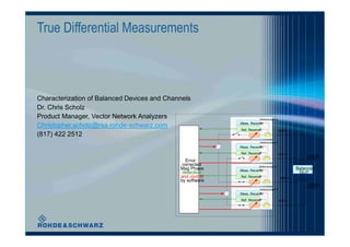
  • 1. True Differential Measurements Characterization of Balanced Devices and Channels Dr. Chris Scholz Product Manager, Vector Network Analyzers Reflectometer 2 Christopher.scholz@rsa.rohde-schwarz.com Meas. Receiver Ref. Receiver PORT 2 (817) 422 2512 Reflectometer 4 Meas. Receiver Ref. Receiver PORT 4 Logical Error PORT 2 corrected Reflectometer 1 Mag Phase Meas. Receiver Balanced detection DUT and control Ref. Receiver PORT 1 by software Logical PORT 1 Reflectometer 3 Meas. Receiver Ref. Receiver PORT 3
  • 2. Outline Reflectometer 2 Meas. Receiver Ref. Receiver PORT 2 Reflectometer 4 Meas. Receiver Ref. Receiver ı Introduction to Signal Integrity PORT 4 Logical Error PORT 2 corrected Reflectometer 1 Mag Phase Balanced  Timing detection Meas. Receiver DUT and control Ref. Receiver  Signal Quality PORT 1 by software Logical ı Balanced Architectures Reflectometer 3 PORT 1 Meas. Receiver  The need for balanced architectures Ref. Receiver PORT 3  Ideal vs. non-ideal devices ı Measurement Techniques for Balanced Architectures  Single mode vs. Differential Mode  Mixed mode S-Parameters Trc18 Sdd21 dB Mag 0.5 dB / Ref -23 dB Ch1 Cal int Trc21 Sdd21 dB Mag 0.5 dB / Ref -23 dB Ch2 Cal int 2 of 16 (Max)  TureDifferential vs. Virtual Differential Sdd21 -20.0  TruDifferential Vector Network Analyzer -20.5 ı Experimental Examples -21.0 -21.5 -22.0 -22.5 -23.0 -23.5 -24.0 Ch1 Start -25 dBm — Freq 1 GHz Stop 0 dBm 1/29/2013 Ch2 Start -28 dBm — 2 Freq 1 GHz Stop -3 dBm 3/8/2007, 1:10 PM
  • 3. Introduction – Signal Integrity ı What is Signal Integrity?  Signal integrity or SI is a set of measures of the quality of an electrical signal.  If the PCB or package already exists, the designer can also measure the impairment presented by the connection using high speed instrumentation such as a vector network analyzer. For example, IEEE P802.3ap Task Force uses measured S-parameters as test cases[9] for proposed solutions to the problem of 10 Gbit/s Ethernet over backplanes.  (Source: Wikipedia, last accessed 01/29/2013) ı Two Key Aspects of SI: Timing Signal Quality 1/29/2013 3
  • 4. Introduction – Signal Integrity ı Timing  Jitter  RJ, DJ, SJ, PJ, DDJ, DCD, ISI, etc.  interconnect flight time vs bit period  chip-to-chip vs on-chip  packaging 1/29/2013 4
  • 5. Introduction - Signal Integrity ı Signal Quality Noise = (S+N)-S  Ringing 10  Cross talk 8  Distortion 6  Ground Bounce 4 amplitude  Ground Noise 2  Signal Loss 0  Power Supply Noise -2 -4 -6 time 1/29/2013 5
  • 6. Introduction – Signal Integrity ı Reflection Noise  Caused by impedance mismatch, vias, interconnect discontinuities ı Crosstalk Noise  Caused by electromagnetic coupling between traces and vias ı Power and Ground Noise  Caused switching noise of the power and ground delivery systems ı EMC/EMI Susceptibility 1/29/2013 6
  • 8. Differential Signaling Unbalanced Device/Channel Balanced (differential) Device/Channel c a 2 1 1 2 b d • Signals referring to ground ı Signals with equal amplitude but 180° phase shift • Also supports a common-mode (in-phase) signal • Virtual ground
  • 9. Balanced devices - Why balanced design? ı Advantages: ı High noise immunity  Minimizes Power and ground plane noise  Minimizes EMI susceptibility  Minimizes Cross talk Components with balanced design: ı Low radiated noise ı High integration density • Amplifiers ı Lower power • Mixers consumption • Filters (e.g. SAW filters) • PCB layout in mobile phones • LAN adapters, converters, filters • PC components (HDD control, etc) • Almost all signals high-speed serial data signals
  • 10. Ideal Balanced Device Characteristics Gain = 1 Differential-mode signal Fully balanced Common-mode signal (EMI or ground noise) Gain = 1 Differential-mode signal Balanced to single ended Common-mode signal (EMI or ground noise) Ideally, balanced devices transmit differential and reject common-mode signals 1/29/2013 10
  • 11. Non-Ideal Balanced Device Characteristics Differential to common- ı Non-ideal balanced devices convert modes mode conversion + Generates EMI Susceptible to EMI Common-mode to differential conversion 1/29/2013 11
  • 12. Non-Ideal Balanced Device Characteristics ı Non-ideal balanced devices convert input modes Differential to common- mode conversion Common-mode to differential conversion 1/29/2013 12
  • 13. Measurement Techniques for Balanced Devices 1/29/2013 13
  • 14. Parameters to Test for a Balanced Device ı Performance in pure differential mode ı Performance in pure common mode ı Conversion from differential mode to common mode (in both directions) ı Conversion from common mode to differential mode (in both directions) 1/29/2013 14
  • 15. Balanced Devices Characteristics ı Real Devices  Propagation of both common mode and differential mode signals  Mode conversion due to non-symmetric design  Susceptability of noise (mainly common mode)  Detailed insight of differential/common mode response required ı Description of balanced devices via special type of S-Parameters:  Mixed-Mode S-Parameters 1/29/2013 15
  • 16. Challenge when measuring balanced devices ı Network analyzers are unbalanced ı Classic Network Analyzers are 2-port instruments ı No balanced calibration standards ı No standard reference impedance (Z0) for balanced device ı Characterization of common and differential transmission model 1/29/2013 16
  • 17. Measurement with Physical BalUns Measurement with differential mode signals at a balanced device Unbalanced network analyzer DUT Balun 1/29/2013 17
  • 18. Measurement with Physical Transformers Measurement with common Unbalanced mode signals at a balanced network analyzer device DUT 1/29/2013 18
  • 19. Balanced Device Characteristics Balun setup for Mixed-Mode-Characterization bal DUT bal unbal unbal Each 2-port combination between balanced and unbalanced ports is necessary for complete mixed mode characterization.
  • 20. Balanced Device Characteristics Physical BalUns: Disadvantages ı Calibration plane different from desired measurement plane ı Degradation of measurement accuracy due to poor RF performance ı Different configurations for different modes necessary (e.g. differential to common-mode conversion) ı Limited in frequency range ı Solution:  Us ideal (virtual) transformer to characterize mixed mode S-parameters of the DUT using virtual, ideal transformers Modal Decomposition Method Use True Differential Method 1/29/2013 20
  • 21. Basic Architecture: Definition of Differential Measuremets Measurement Principle ı VirDi = Virtual differential Mode  Characterization of balanced DUT as single ended DUT with mathematical calculation of mixed-mode S-Parameters form single ended S-Parameters ı TruDi = True differential Mode  Stimulation of DUT with true differential and common mode signals with calculation of mixed-mode S-Parameters from error corrected mixed mode wave quantities 1/29/2013 21
  • 22. Virtual Differential Measurement ı Subsequent single ended measurements with post processing using linear superposition ı Applicable for all passive devices and active devices operating in their linear region ı Large deviations compared to TruDi in large signal operation, especially in terms of compression curve characteristics  Nonlinear behavior of the DUT forbids linear superposition 1/29/2013 22
  • 23. True Differential Measurement ı The DUT is stimulated using a real differential mode or real common mode signal ı Better accuracy in small signal operation ı Accurately measure compression under large signal operation 1/29/2013 23
  • 24. ZVA – True Differential Mode ı Coherent sources  Generation of true differential and common mode stimulus signals  At least one signal output can be adjusted in amplitude and phase with respect to the other ı Simultaneous measurement of two reference signals (a waves) and two measurement signals (b waves) ı Four-port calibration in the reference plane  Vector-corrected measurement of a single ended waves or voltages (a and b waves) ı Calculation of true differential S-Parameters from vector corrected wave quantities 1/29/2013 24
  • 25. A True Differential Network Analyzer Reflectometer 2 Meas. Receiver Ref. Receiver PORT 2 Reflectometer 4 Meas. Receiver Ref. Receiver PORT 4 Logical PORT 2 Error corrected Reflectometer 1 Mag Phase Balanced Meas. Receiver detection DUT and control Ref. Receiver PORT 1 by software Logical PORT 1 Reflectometer 3 Meas. Receiver Ref. Receiver PORT 3 1/29/2013 25
  • 26. True Differential Measurements with R&S Network Analyzers ZVA and ZVT 1/29/2013 26
  • 27. Sweep modes (R&S®ZVA-K6) differential mode 180° common mode 0° Coherent signals of arbitrary phase and amplitude imbalance are possible  Sweep Modes:  Frequency  Phase (Phase of the stimulating signal can be swept from 0° to 180° )  Magnitude (Variation of the relative magnitude of the differential signals)  “Classical” calibration techniques sufficient (full two port)  Investigation of the DUT under real conditions 1/29/2013 27
  • 28. Typical measurements quality parameters ı Differential and common mode insertion loss ı Differential and common mode return loss ı NEXT-Measurements (Near End Crosstalk) ı FEXT-Measurements (Far End Crosstalk) ı Amplitude-Imbalance ı Phase-Imbalance ı Common-Mode Rejection Ratio (CMRR) 1/29/2013 28
  • 29. True Differential vs. Virtual Differential TruDi vs. VerDi 1/29/2013 29
  • 30. Modal Decomposition Method Principle 4-port device with Description of virtual 16 measured ideal transformers unbalanced S- parameter Calculated mixed mode S-parameters ı Calculation of the mixed mode S-parameters using unbalaced S-Parameters and virtual transformers 1/29/2013 30
  • 31. Modal Decomposition Method test fixture a Port 1 Port 3 a DUT DUT b b Port 2 Port 4  a 1   S 11 S 12 S 13 S 14  b 4        a 2   S 2 1 S 22 S 23 S 24   b 3  a  S S S S  b   3   31 32 33 34   2  a 4  S 4 1    S 42 S 43 S 44    b 1   ı Measure the balanced 2-port device as unbalanced 4-port device with unbalanced VNA 1/29/2013 31
  • 32. Solution: Modal Decomposition Method [Z] [P], [Q] [Zm] ı Calculate the mixed mode Zm-parameters of the combination of DUT with transformers. 1/29/2013 32
  • 33. Port Configurations Mixed Mode DUT ı Physical single ending ports  logical balanced ports Port 3 Port 1 Port 4 Port 2 physical ports DUT logical ports Port 1 Port 2 ı Different impedances for common-mode and differential-mode  differential-mode (ideally matched)  100 ( =2*Z0 )  common-mode (ideally matched)  25 ( = 1/2*Z0 ) 1/29/2013 33
  • 34. Modal Decomposition Method Mixed Mode S-Parameter Matrix DU Differential-Mode stimulus Common-Mode stimulus T Port 1 Port 2 Port 1 Port 2 Logical Port 1 Logical Port 2 Differential- Port 1  S dd11 S d d1 2 S dc11 S dc12  mode Port 2 S S dd 22 S dc 21 S d c 22  Response  dd 21  Common- Port 1  S cd11 S cd12 S cc1 1 S cc12  mode Port 2   Response  S cd 21  S cd 22 S cc 21 S cc 22  Naming Convention: S mode res., mode stim., port res., port stim. 1/29/2013 34
  • 35. Mixed Mode S-Matrix: DD Quadrant input reflection reverse transmission  S dd 11 S dd 12 S dc 11 S dc 12     S dd 21 S dd 22 S dc 21 S dc 22   S cd 11 S cd 12 S cc 11 S cc 12     S cd 21 S cd 22 S cc 21 S cc 22  forward transmission output reflection ı Describes fundamental performance in pure differential-mode operation 1/29/2013 35
  • 36. Mixed Mode S-Matrix: CC Quadrant input reflection reverse transmission  S dd 11 S dd 12 S dc 11 S dc 12     S dd 21 S dd 22 S dc 21 S dc 22   S cd 11 S cd 12 S cc 11 S cc 12     S cd  21 S cd 22 S cc 21 S cc 22   forward transmission output reflection ı Describes fundamental performance in pure common-mode operation 1/29/2013 36
  • 37. Mixed Mode S-Matrix: DC Quadrant input reflection reverse transmission  S dd 11 S dd 12 S dc 11 S dc 12     S dd 21 S dd 22 S dc 21 S dc 22   S cd 11 S cd 12 S cc 11 S cc 12     S cd  21 S cd 22 S cc 21 S cc 22   forward transmission output reflection ı Describes conversion of a common-mode stimulus to a differential-mode response ı Terms are ideally equal to zero with perfect symmetry ı Related to the generation to EMI 1/29/2013 37
  • 38. Mixed Mode S-Matrix: CD Quadrant input reflection reverse transmission  S dd 11 S dd 12 S dc 11 S dc 12     S dd 21 S dd 22 S dc 21 S dc 22   S cd 11 S cd 12 S cc 11 S cc 12     S cd  21 S cd 22 S cc 21 S cc 22   forward transmission output reflection ı Describes conversion of a differential-mode stimulus to a common-mode response ı Terms are ideally equal to zero with perfect symmetry ı Related to the susceptibility of EMI 1/29/2013 38
  • 39. 3-Port device single ended  common / differential-mode Single-ended differential-mode common-mode Port 1 Port 2 (unbalanced) DUT (balanced) Single Diff.- Com.- Ended mode mode Stim. Stim. Stim. Port 1 Port 2 Port 2 Single-ended Response Port 1  Sss11 Ssd12 Ssc12  S Sdc22   ds21 Sdd22 Differential - Port 2 Mode Response  common-mode Port 2 Scs 21 Scd 22  Scc22   Response 1/29/2013 39
  • 40. Measurement Examples: TrueDi vs. VirDi 1/29/2013 40
  • 41. Instrument Control of TruDi 1. Apply full n-port calibration, e.g. with CalUnit 2. Configure balanced Measurement 3. Switch to True differential Mode 1/29/2013 41
  • 42. Special Features of TruDi ı Simultaneous display of VirDi and TruDi S-Parameters ı Same “calibration” for VirDi and TruDi ı Measurement of error corrected S-Parameters and wave quantities (measure diff/comm power with diff/comm stimulation) ı Phase imbalance sweep  P, f : fixed   (max) = -180° to +180° ı Magnitude imbalance sweep  f : fixed  P(max) = -10 dB to + 10 dBm (max)
  • 43. ZVA Coherent Sources ı Coherence Mode  allows to set an arbitrary phase and amplitude between the R&S®ZVA’s signals sources ı R&S®ZVA-K6 True Differential Option ı Applications:  Modulators  Antenna beam forming ı Realtime measurement ı In R&S®ZVA67 four individual phase shifts
  • 44. Example 1: Tunable Active Filter Trc18 Sdd21 dB Mag 0.5 dB / Ref -23 dB Ch1 Cal int 2 of 16 (Max) Trc21 Sdd21 dB Mag 0.5 dB / Ref -23 dB Ch2 Cal int Sdd21 -20.0 -20.5 -21.0 Gain compression -21.5 true differential -22.0 -22.5 -23.0 virtual differential -23.5 -24.0 Ch1 Start -25 dBm — Freq 1 GHz Stop 0 dBm Ch2 Start -28 dBm — Freq 1 GHz Stop -3 dBm 3/8/2007, 1:10 PM True differential power axis has been shifted by -3 dB to equalize voltage amplitudes 1/29/2013 44
  • 45. Tunable Active Filter Trc18 Sdd21 dB Mag 2 dB / Ref -10 dB Ch1 Cal 2 of 16 (Max) Trc21 Sdd21 dB Mag 2 dB / Ref -10 dB Ch2 Cal int Sdd21 -2 -4 Trc18 Sdd21 dB Mag 2 dB / Ref -10 dB Ch1 Cal 2 of 16 (Max) Trc21 Sdd21 dB Mag 2 dB / Ref -10 dB Ch2 Cal int -6 Sdd21 -8 -2 -10 -4 -12 -6 -14 -8 -16 -10 -18 -12 -14 Ch1 Start 10 MHz — Pwr -20 dBm Stop 2 GHz Ch2 Start 10 MHz — Pwr -23 dBm Stop -16 2 GHz 3/8/2007, 1:20 PM -18 Ch1 Start 10 MHz — Pwr -10 dBm Stop 2 GHz Ch2 Start 10 MHz — Pwr -13 dBm Stop 2 GHz 3/8/2007, 1:19 PM • No difference between modes at low power (left), • Higher gain for true mode at high power (right) 1/29/2013 45
  • 46. S-Parameters vs. Input Power Trc18 Sdd21 dB Mag 5 dB / Ref 0 dB Ca? 1 Trc19 Sdd21 dB Mag 5 dB / Ref 0 dB Cal int 2 Mkr 2 Sdd21 20 Mkr 1 6.96 dBm -4.893 dB Mkr Sdd21 2 20 Mkr 1 6.96 dBm -0.571 dB Mkr 2 -29.76 dBm 16.145 dB Mkr 2 -29.76 dBm 16.577 dB 10 10 Mkr 1 0 Mkr 1 0 -10 -10 -20 -20 Ch3 Start -30 dBm Freq 1 GHz Stop 11 dBm Ch4 Start -30 dBm Freq 1 GHz Stop 11 dBm Trc20 Scd21 dB Mag 5 dB / Ref -5 dB Ca? 3 Trc21 Scd21 dB Mag 5 dB / Ref -5 dB Cal int 4 Mkr Scd21 215 •Mkr 1 6.96 dBm -16.735 dB Mkr Scd21 215 Mkr 1 6.96 dBm -12.183 dB Mkr 2 -29.76 dBm 6.742 dB Mkr 2 -29.76 dBm 7.575 dB 5 5 -5 -5 Mkr 1 Mkr 1 -15 -15 -25 -25 Ch3 Start -30 dBm Freq 1 GHz Stop 11 dBm Ch4 Start -30 dBm Freq 1 GHz Stop 11 dBm Trc22 Scc21 dB Mag 1 dB / Ref -9 dB Ca? 5 Trc23 Scc21 dB Mag 1 dB / Ref -9 dB Cal int 6 Scc21 -5 Mkr 1 6.96 dBm -6.733 dB Scc21 -5 Mkr 1 6.96 dBm -8.351 dB Mkr 1 Mkr 2 -29.76 dBm -9.186 dB Mkr 2 -29.76 dBm -8.244 dB -7 Mkr 2 -7 Mkr 1 Mkr 2 -9 -9 -11 -11 -13 -13 Ch3 Start -30 dBm Freq 1 GHz Stop 11 dBm Ch4 Start -30 dBm Freq 1 GHz Stop 11 dBm virtual differential mode true differential mode 1/29/2013 46
  • 47. Phase Imbalance Sweep Trc11 Sdd21 dB Mag 1 dB / Ref -5 dB Cal int 5 of 3 (Max) Trc12 ac1 dB Mag 10 dB / Ref 0 dBm Cal int Trc13 ad1 dB Mag 10 dB / Ref 0 dBm Cal int ad1 Mkr 1 0.000000 ° -2.339 dB Mkr 1 0.000000 ° -57.751 dBm 10 0 Mkr 1 -10 -20 -30 -40 -50 Mkr 1 -60 -70 Ch7 Phas Imb Start -180° Freq 1 GHz Pwr 0 dBm Stop 180° 1/29/2013 47
  • 48. Phase & Magnitude Imbalance Sweep Trc1 Sdd21 dB Mag 1 dB / Ref 10 dB Ch1 Cal int 1 of 1 (Max) Trc2 Sdd21 dB Mag 1 dB / Ref 10 dB Ch2 Cal int Trc3 bd2 dB Mag 0.5 dB / Ref 3 dBm Ch1 Cal int Sdd21 15 14 13 12 11 10 9 8 7 Ch1 Ampl Imb Start -10 dB — —Freq 1 GHz Pwr -10 dBm Stop 10 dB Ch2 Phas Imb Start -180° — Freq 1 GHz Pwr -10 dBm Stop 180° 1/23/2007, 4:54 PM 1/29/2013 48
  • 49. Theoretical Verification ı Approach:  A model based analysis  Analytical calculations using MATLAB  Experimental Verification  Measurements ı DUT  The most simple bipolar differential amplifier
  • 50. Modeling the DUT ı The two inputs / outputs can be regarded as common / differential inputs and outputs Gain of the individual amplifier Compression and 3rd order intermodulation Sdd 21 ı a1 & afb determine the CMRR CMRR   ratio between differential mode and common mode voltage gain Scc 21 1/29/2013 50
  • 51. Modeling the DUT ı Feedback factor afb 1/29/2013 51
  • 52. Modeling the DUT ı Does not include a shared feed back (CMRR 0) ı A system of two independent, ideally identical single-ended amplifiers ı VirDi leads to underestimation! Input referred 1-dB compression point 1/29/2013 52
  • 53. TruDi « VirDi ideal differential pair I current sourced differential pair (CMRR ®∞) I VirDi leads to overestimation! 1/29/2013 53
  • 54. Experimental Verification: Amplifier Test Circuit RE = 0  CMRR  0dB RE = 27W  CMRR 16dB 1/29/2013 54
  • 56. Experimental Verification: Measurement Results 2,4dB 16dB 1/29/2013 56
  • 57. Experimental Verification: Low CMRR Trc1 Sdd21 dB Mag 10 dB / Ref 0 dB Ch1 Cal 1 of 1 (Max) Trc2 Scc21 dB Mag 10 dB / Ref 0 dB Ch2 Cal Sdd21 • M 1 600.00000 MHz 9.1983 dB 40 M 1 600.00000 MHz 3.8022 dB 30 20 M1 10 M1 0 -10 -20 -30 -40 Ch1 TrD Start 10 MHz — Pwr -25 dBm Stop 2 GHz Ch2 TrD Start 10 MHz — Pwr -25 dBm Stop 2 GHz 1/29/2013 57
  • 58. Experimental Verification: High CMRR Trc1 Sdd21 dB Mag 10 dB / Ref 0 dB Ch1 Cal 1 of 1 (Max) Trc2 Scc21 dB Mag 10 dB / Ref 0 dB Ch2 Cal Sdd21 • M 1 600.00000 MHz 9.2649 dB 40 M 1 600.00000 MHz -26.255 dB 30 20 M1 10 0 -10 -20 M1 -30 -40 Ch1 TrD Start 10 MHz — Pwr -25 dBm Stop 2 GHz Ch2 TrD Start 10 MHz — Pwr -25 dBm Stop 2 GHz 8/11/2010 4 39 PM 1/29/2013 58
  • 59. Experimental Verification: Low CMRR Trc1 Sdd21 dB Mag 2 dB / Ref 4 dB Ch1 Cal int PCai 1 of 1 (Max) Trc2 Sdd21 dB Mag 2 dB / Ref 4 dB Ch2 Ca? PCai Trac Stat: Trc1 Sdd21 Sdd21 Cmp In: -4.3 dBm 12 Cmp Out: 3.9 dBm •Trac Stat: Trc2 Sdd21 10 Cmp In: -4.7 dBm Cmp Cmp Out: 3.3 dBm Cmp 8 6 4 2 0 -2 -4 Ch1 TrD Start -25 dBm — Freq 600 MHz Stop 10 dBm Ch2 Start -25 dBm — Freq 600 MHz Stop 10 dBm 1/29/2013 59
  • 60. Experimental Verification: High CMRR Trc1 Sdd21 dB Mag 2 dB / Ref 4 dB Ch1 Cal int PCai 1 of 1 (Max) Trc2 Sdd21 dB Mag 2 dB / Ref 4 dB Ch2 Ca? PCai Trac Stat: Trc1 Sdd21 Sdd21 Cmp In: -4.1 dBm 12 Cmp Out: 4.2 dBm •Trac Stat: Trc2 Sdd21 10 Cmp In: -1.0 dBm Cmp Cmp Out: Cmp 7.1 dBm 8 6 4 2 0 -2 -4 Ch1 TrD Start -25 dBm — Freq 600 MHz Stop 10 dBm Ch2 Start -25 dBm — Freq 600 MHz Stop 10 dBm 1/29/2013 60
  • 61. Summary and Conclusions 1/29/2013 61
  • 62. Summary: TruDi vs. VirDi ı Passive Devices/Linear operation  TruDi and VirDi give exactly the same results ı Active Devices/Non-linear operation  Significant difference between TruDi and VirDi  TruDi represents the real operating conditions of a device ı TruDi Measurements  Requires two (or more) phase coherent sources  Ability to scan amplitude and phase independently  Relative phase stability of VNA sources is crucial for reproducible results 1/29/2013 62
  • 63. Thank you for your Attention More information Rohde & Schwarz boot # 701 http://www.rohde-schwarz.com Chris Scholz Christopher.scholz@rsa.rohde-schwarz.com (817) 422 2512
  • 64. Appendix: De/Embedding 1/29/2013 64
  • 65. (De)Embedding - Matching Networks ı Challenges of Fixtures  Mask true device behavior  No well characterized ı Disadvantages of Physical Matching Networks:  Poor reproducibility  Narrow band  Restricted to low frequencies  Inflexible (one network for one frequency range) ı Use of theoretically Embedded Matching Networks:  Both Embedding and Deembedding  Highest degree of flexibility to integrate networks  No frequency restriction  Possible disadvantages just with active devices 1/29/2013 65
  • 66. Introduction: Embedding DUT DUT + Test Fixture + Matching Networks Matching Networks  not present as hardware  but represented by calculation Available Networks: network analyzer 1 DUT • Import of arbitrary S-parameter files Port 2 Port 1 • Use of predefined matching networks DUT DUT + Test Fixture
  • 67. Introduction: Deembedding Response of networks network analyzer  not corrected by calibration  corrected by calculation w/o calibration or deembedding w/o calibration or deembedding Reference plane at POR T 1 Reference plane at POR T 2 DUT Response of test fixture, strip lines etc. • Import of S-parameter files (gained e.g. using a SW design tool) • Use of predefined networks Shift of reference plane by Deembedding (or alternatively via calibration)
  • 68. (De)Embedding Networks (single ended DUTs) Single Ended Port (De)Embedding  Import of *.s2p files ı 8 predefined networks
  • 69. (De)Embedding Networks (single ended DUTs) Pre-defined matching networks
  • 70. (De)Embedding Networks (differential DUTs) Balanced Port (De)Embedding ı Import of *.s4p files  12 predefined networks
  • 71. (De)Embedding Networks (differential DUTs) Pre-defined matching networks
  • 72. Appendix 2: Measurement Wizard 1/29/2013 72
  • 73. Measurement Wizard Step 1 : Selection of test configuration
  • 74. Measurement Wizard Step 2 : Impedance Settings
  • 75. Measurement Wizard Step 3 : Selection of S-Parameters
  • 76. Measurement Wizard Step 4 : General Settings
  • 77. Measurement Wizard Step 5 : Bandwidth and Power Setting
  • 78. Measurement Wizard Step 6 : Calibration
  • 79. Measurement Result (1) Measurement result of SAW Filter
  • 80. Measurement Result (2) Automatic Amplitude and Phase Imbalance Measurement