Download as PDF, PPTX
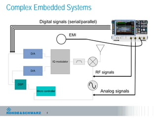
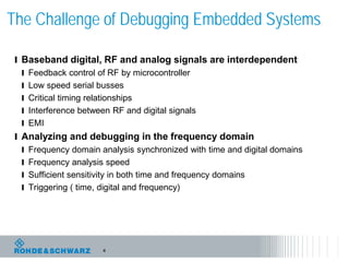
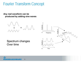
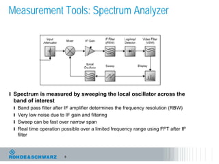
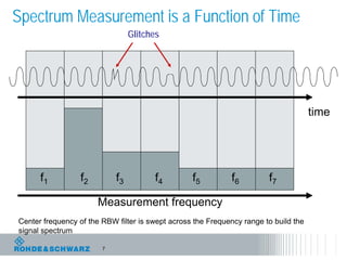
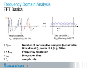
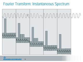
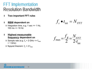
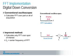
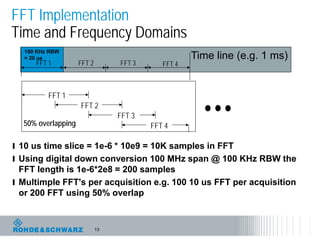
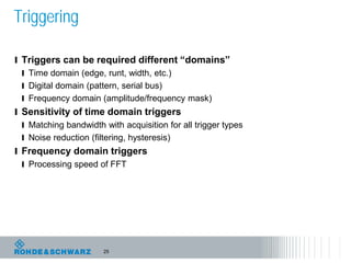
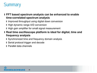

The document discusses the complexities of debugging embedded systems through synchronous time and frequency domain analysis, emphasizing the interdependencies of digital, RF, and analog signals. It covers topics including the Fourier transform, measurement tools like spectrum analyzers, and the importance of effective noise reduction and triggering techniques. Additionally, it highlights the improvements in FFT-based spectrum analysis, dynamic range of ADCs, and real-time analysis in integrated digital and analog environments.


![Multiband Transceivers - [Chapter 3] Basic Concept of Comm. Systems](https://cdn.slidesharecdn.com/ss_thumbnails/ch3-150613070933-lva1-app6892-thumbnail.jpg?width=640&height=640&fit=bounds)