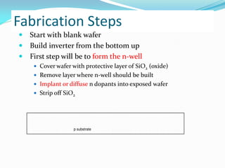
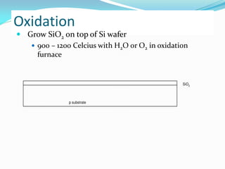
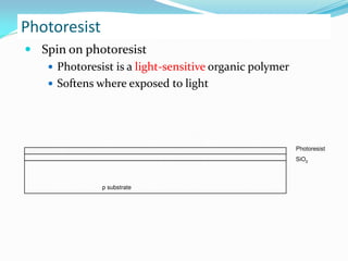
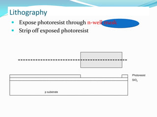
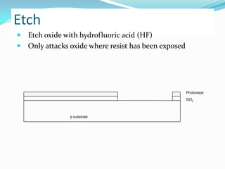
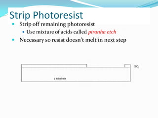
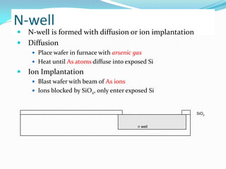
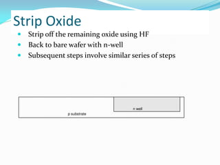
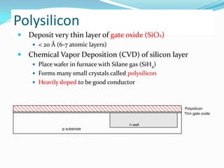
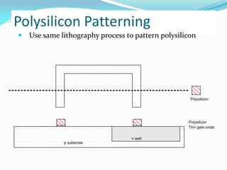
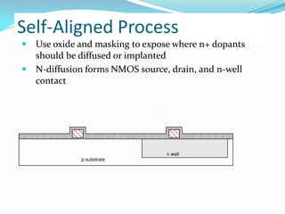
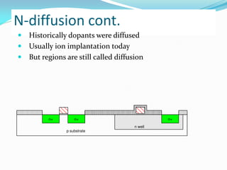
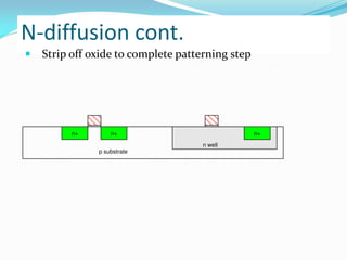
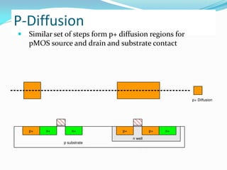
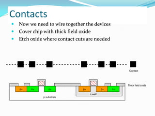
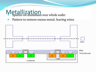
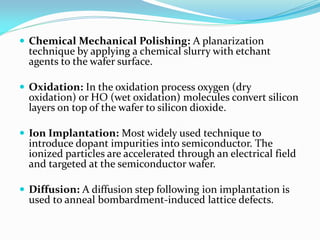
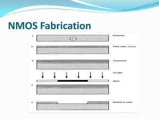
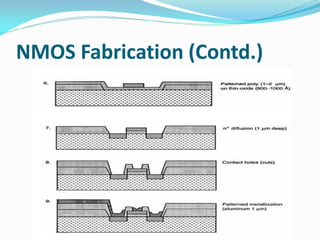
IC Fabrication Process Steps
 The fabrication of integrated circuits consists basically of the following
process steps:
 Lithography: The process for pattern definition by applying thin
uniform layer of viscous liquid (photo-resist) on the wafer surface. The
photo-resist is hardened by baking and than selectively removed by
projection of light through a reticle containing mask information.
 Etching: Selectively removing unwanted material from the surface of
the wafer. The pattern of the photo-resist is transferred to the wafer by
means of etching agents.
 Deposition: Films of the various materials are applied on the wafer.
For this purpose mostly two kind of processes are used, physical vapor
deposition (PVD) and chemical vapor deposition (CVD).
Fabrication Steps
 Start with blank wafer
 Build inverter from the bottom up
 First step will be to form the n-well
 Cover wafer with protective layer of SiO2 (oxide)
 Remove layer where n-well should be built
 Implant or diffuse n dopants into exposed wafer
 Strip off SiO2
p substrate
Oxidation
 Grow SiO2 on top of Si wafer
 900 – 1200 Celcius with H2O or O2 in oxidation
furnace
p substrate
SiO2
Photoresist
 Spin on photoresist
 Photoresist is a light-sensitive organic polymer
 Softens where exposed to light
p substrate
SiO2
Photoresist
Lithography
 Expose photoresist through n-well mask
 Strip off exposed photoresist
p substrate
SiO2
Photoresist
Etch
 Etch oxide with hydrofluoric acid (HF)
 Only attacks oxide where resist has been exposed
p substrate
SiO2
Photoresist
Strip Photoresist
 Strip off remaining photoresist
 Use mixture of acids called piranha etch
 Necessary so resist doesn’t melt in next step
p substrate
SiO2
N-well
 N-well is formed with diffusion or ion implantation
 Diffusion
 Place wafer in furnace with arsenic gas
 Heat until As atoms diffuse into exposed Si
 Ion Implantation
 Blast wafer with beam of As ions
 Ions blocked by SiO2, only enter exposed Si
n well
SiO2
Strip Oxide
 Strip off the remaining oxide using HF
 Back to bare wafer with n-well
 Subsequent steps involve similar series of steps
p substrate
n well
Polysilicon
 Deposit very thin layer of gate oxide (SiO2)
 < 20 Å (6-7 atomic layers)
 Chemical Vapor Deposition (CVD) of silicon layer
 Place wafer in furnace with Silane gas (SiH4)
 Forms many small crystals called polysilicon
 Heavily doped to be good conductor
Thin gate oxide
Polysilicon
p substrate
n well
Polysilicon Patterning
 Use same lithography process to pattern polysilicon
Polysilicon
p substrate
Thin gate oxide
Polysilicon
n well
Self-Aligned Process
 Use oxide and masking to expose where n+ dopants
should be diffused or implanted
 N-diffusion forms NMOS source, drain, and n-well
contact
p substrate
n well
N-diffusion
 Pattern oxide and form n+ regions
 Self-aligned process where gate blocks diffusion
 Polysilicon is better than metal for self-aligned gates because it
doesn’t melt during later processing
p substrate
n well
n+ Diffusion
N-diffusion cont.
 Historically dopants were diffused
 Usually ion implantation today
 But regions are still called diffusion
n well
p substrate
n+
n+ n+
N-diffusion cont.
 Strip off oxide to complete patterning step
n well
p substrate
n+
n+ n+
P-Diffusion
 Similar set of steps form p+ diffusion regions for
pMOS source and drain and substrate contact
p+ Diffusion
p substrate
n well
n+
n+ n+
p+
p+
p+
Contacts
 Now we need to wire together the devices
 Cover chip with thick field oxide
 Etch oxide where contact cuts are needed
p substrate
Thick field oxide
n well
n+
n+ n+
p+
p+
p+
Contact
Metallization
 Sputter on aluminum over whole wafer
 Pattern to remove excess metal, leaving wires
p substrate
Metal
Thick field oxide
n well
n+
n+ n+
p+
p+
p+
Metal
 Chemical Mechanical Polishing: A planarization
technique by applying a chemical slurry with etchant
agents to the wafer surface.
 Oxidation: In the oxidation process oxygen (dry
oxidation) or HO (wet oxidation) molecules convert silicon
layers on top of the wafer to silicon dioxide.
 Ion Implantation: Most widely used technique to
introduce dopant impurities into semiconductor. The
ionized particles are accelerated through an electrical field
and targeted at the semiconductor wafer.
 Diffusion: A diffusion step following ion implantation is
used to anneal bombardment-induced lattice defects.
NMOS Fabrication
NMOS Fabrication (Contd.)

Fabrication

  • 2.
    IC Fabrication ProcessSteps  The fabrication of integrated circuits consists basically of the following process steps:  Lithography: The process for pattern definition by applying thin uniform layer of viscous liquid (photo-resist) on the wafer surface. The photo-resist is hardened by baking and than selectively removed by projection of light through a reticle containing mask information.  Etching: Selectively removing unwanted material from the surface of the wafer. The pattern of the photo-resist is transferred to the wafer by means of etching agents.  Deposition: Films of the various materials are applied on the wafer. For this purpose mostly two kind of processes are used, physical vapor deposition (PVD) and chemical vapor deposition (CVD).
  • 3.
    Fabrication Steps  Startwith blank wafer  Build inverter from the bottom up  First step will be to form the n-well  Cover wafer with protective layer of SiO2 (oxide)  Remove layer where n-well should be built  Implant or diffuse n dopants into exposed wafer  Strip off SiO2 p substrate
  • 4.
    Oxidation  Grow SiO2on top of Si wafer  900 – 1200 Celcius with H2O or O2 in oxidation furnace p substrate SiO2
  • 5.
    Photoresist  Spin onphotoresist  Photoresist is a light-sensitive organic polymer  Softens where exposed to light p substrate SiO2 Photoresist
  • 6.
    Lithography  Expose photoresistthrough n-well mask  Strip off exposed photoresist p substrate SiO2 Photoresist
  • 7.
    Etch  Etch oxidewith hydrofluoric acid (HF)  Only attacks oxide where resist has been exposed p substrate SiO2 Photoresist
  • 8.
    Strip Photoresist  Stripoff remaining photoresist  Use mixture of acids called piranha etch  Necessary so resist doesn’t melt in next step p substrate SiO2
  • 9.
    N-well  N-well isformed with diffusion or ion implantation  Diffusion  Place wafer in furnace with arsenic gas  Heat until As atoms diffuse into exposed Si  Ion Implantation  Blast wafer with beam of As ions  Ions blocked by SiO2, only enter exposed Si n well SiO2
  • 10.
    Strip Oxide  Stripoff the remaining oxide using HF  Back to bare wafer with n-well  Subsequent steps involve similar series of steps p substrate n well
  • 11.
    Polysilicon  Deposit verythin layer of gate oxide (SiO2)  < 20 Å (6-7 atomic layers)  Chemical Vapor Deposition (CVD) of silicon layer  Place wafer in furnace with Silane gas (SiH4)  Forms many small crystals called polysilicon  Heavily doped to be good conductor Thin gate oxide Polysilicon p substrate n well
  • 12.
    Polysilicon Patterning  Usesame lithography process to pattern polysilicon Polysilicon p substrate Thin gate oxide Polysilicon n well
  • 13.
    Self-Aligned Process  Useoxide and masking to expose where n+ dopants should be diffused or implanted  N-diffusion forms NMOS source, drain, and n-well contact p substrate n well
  • 14.
    N-diffusion  Pattern oxideand form n+ regions  Self-aligned process where gate blocks diffusion  Polysilicon is better than metal for self-aligned gates because it doesn’t melt during later processing p substrate n well n+ Diffusion
  • 15.
    N-diffusion cont.  Historicallydopants were diffused  Usually ion implantation today  But regions are still called diffusion n well p substrate n+ n+ n+
  • 16.
    N-diffusion cont.  Stripoff oxide to complete patterning step n well p substrate n+ n+ n+
  • 17.
    P-Diffusion  Similar setof steps form p+ diffusion regions for pMOS source and drain and substrate contact p+ Diffusion p substrate n well n+ n+ n+ p+ p+ p+
  • 18.
    Contacts  Now weneed to wire together the devices  Cover chip with thick field oxide  Etch oxide where contact cuts are needed p substrate Thick field oxide n well n+ n+ n+ p+ p+ p+ Contact
  • 19.
    Metallization  Sputter onaluminum over whole wafer  Pattern to remove excess metal, leaving wires p substrate Metal Thick field oxide n well n+ n+ n+ p+ p+ p+ Metal
  • 20.
     Chemical MechanicalPolishing: A planarization technique by applying a chemical slurry with etchant agents to the wafer surface.  Oxidation: In the oxidation process oxygen (dry oxidation) or HO (wet oxidation) molecules convert silicon layers on top of the wafer to silicon dioxide.  Ion Implantation: Most widely used technique to introduce dopant impurities into semiconductor. The ionized particles are accelerated through an electrical field and targeted at the semiconductor wafer.  Diffusion: A diffusion step following ion implantation is used to anneal bombardment-induced lattice defects.
  • 21.
  • 22.