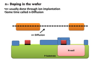
The document summarizes the fabrication process for integrated circuits using N-well fabrication. It involves taking a P-substrate wafer and growing a silicon dioxide layer through oxidation. Photolithography is used to pattern the wafer by applying a photoresist, exposing it to UV light through a mask, and etching away exposed areas. An N-well is formed through ion implantation and diffusion. Further steps involve growing a thin gate oxide, depositing polysilicon and patterning it, and doing self-aligned N+ and P+ ion implantations to form sources and drains. Metallization is done and contacts are formed to connect transistors, resulting in an NMOS and PMOS on the chip.