- The document provides a full reverse costing analysis of the Transphorm TPH3206PS 600V GaN-on-silicon HEMT power transistor.
- The analysis includes detailed photos and SEM analysis of the epitaxial layers and transistor structure, as well as an examination of the Quiet-Tab packaging.
- The manufacturing process flows for the GaN HEMT, resistor, MOSFET, and packaging are presented, along with an in-depth cost breakdown analysis.
- Estimates of the manufacturing cost and suggested manufacturer price are provided, and comparisons are made to Transphorm's TPH3002 and GaN Systems' GS66504B.
Transphorm TPH3002PS 600V GaN on Silicon HEMT 2015 teardown reverse costing r...Yole Developpement
High voltage GaN HEMT developed for the high frequency operation in a low-inductance source terminal TO220 package
The TPH3002PS is a 600V EZ-GaN™ HEMT for high frequency operations from Transphorm. Manufactured by Fujitsu and assembled in a TO220 package, it features the Quiet-TabTM scheme which increases switching speed by 200%. With a 7.5ns turn-on and a 10ns turn-off, the TPH3002PS has a higher switch frequency than the best CoolMOS.
The TPH3002PS is based on a cascode configuration of a GaN on Silicon HEMT transistor to hold the high voltage and a standard low voltage MOSFET to drive high frequency and to make a normally-off transistor from a normally-on GaN HEMT.
The device is assembled in a TO220 package for an easy integration in converter electronic system. Moreover, it integrates a Quiet-Tab™ and a Gate-Source-Drain (GSD) pin-out arrangement in order to reduce the parasitic inductance and capacitance in high frequency and to allow 200% increase in switching speed compared to traditional TO-220.
The report presents a deep technology analysis of the packaging and the components with TEM images of the complex GaN epitaxy layer stack and transistor structure.
It also includes production cost analysis and overall comparison with GaN Systems GS66508P 650V HEMT.
More information on that report at http://www.i-micronews.com/reports.html
Panasonic PGA26C09DV 600V GaN HEMT teardown reverse costing report published ...Yole Developpement
Panasonic’s first 600V GaN HEMT has an innovative structure designed to integrate a normally-off transistor in a standard package, without a cascade structure
System Plus Consulting unveils Panasonic’s first GaN HEMT, assembled in a standard TO220 package. Thanks to its specific die design, the component is normally-off without using a cascade structure or special packaging.
Panasonic’s PGA26C09DV features a medium-voltage breakdown of 600V for a current of 15A (25°C), with very low RdsOn compared to its competitors. The transistor is optimized for AC-DC power supply, photovoltaic, and motor inverters.
The GaN and AlGaN layers are deposited by epitaxy on a silicon substrate. A complex buffer and template layer structure is used to reduce stress and dislocation. This is complemented by a thick superlattice structure clearly visible in the TEM analysis.
Based on a complete teardown analysis, this report also provides a production cost estimate for the epitaxy, HEMT, and package.
Moreover, this report offers a comparison with GaN Systems’ GS66504B and Transphorm’s GaN HEMT, highlighting the huge differences in design and manufacturing process and their impact on device size and production cost.
For more information visite us at: http://www.i-micronews.com/reports.html
GaN Systems GS61004B GaN HEMT 2018 teardown reverse costing report published ...system_plus
Discover how GaN Systems has designed its high-current, low-voltage PCB embedded GaN-on-Si transistor.
More information on that report at: http://www.systemplus.fr/reverse-costing-reports/gan-systems-gs61004b-gan-hemt/
Rohm SiC MOSFET Gen3 Trench Design Familysystem_plus
Trench technology in Rohm 650V and 1200V SiC MOSFETs.
More information on that report at: http://www.systemplus.fr/reverse-costing-reports/rohm-sic-mosfet-gen3-trench-design-family/
Panasonic 600 V GaN HEMT PGA26E19BA 2017 teardown reverse costing report publ...Yole Developpement
Panasonic adopts a DFN 8x8 package for its normally-off GaN HEMT structure
System Plus Consulting unveils the first GaN HEMT from Panasonic assembled in a dual flat no-lead (DFN) 8x8 package. Panasonic decided to abandon the standard TO220 package, probably because of poor electrical performance. Thanks to its proprietary X-GaN transistor structure and new die design the company has managed to produce a very competitive normally-off component.
The new PGA26E19BA from Panasonic features a medium breakdown voltage of 600V for a current of 10A at 25°C, with very low on-resistance with respect to its competitors and the TO220 assembled component.The transistor is optimized to be used in power supplies and AC-DC, photovoltaic and motor inverters.
Take a look at the fifth generation of EPC’s low voltage transistor
The low voltage GaN device market is increasingly important, and Efficient Power Conversion Corporation (EPC) is a major player in low voltage GaN-on-silicon high-electron-mobility transistor (HEMT) devices. 100V GaN HEMTs are a very new technology but they already compete with silicon transistors, especially in the field of megahertz high frequency applications.
System Plus Consulting has investigated the company’s EPC2045 device, its latest driving 100V for applications such as single-stage 48V converters, USB-C data and power connectors, LiDAR sensors, point-of-load converters and loads in open rack server architectures.
With its new transistor and GaN epitaxy design, the EPC2045 achieves a breakdown voltage of 100V for a current of 16A at 25°C, and a very low RdsOn on-resistance of 7mΩ compared to the previous generation.
The chip-scale packaging of EPC products reduces the final device cost and decreases its inductance, bringing advantages not only with respect to competitors in GaN, but also silicon.
Compared to silicon transistors, GaN process developments have significantly lowered capacitance. This translates into lower gate drive losses and lower device switching losses at higher frequencies for the same on-resistance and voltage rating.
More information on that report at http://www.i-micronews.com/reports.html
GaN-on-Silicon Transistor Comparison 2018 Structural, Process & Costing Repor...Yole Developpement
Dive deep into the technology and cost of GaN-on-silicon HEMTs from EPC, Transphorm, GaN Systems, Panasonic and Texas Instruments.
More information on that report at https://www.i-micronews.com/report/product/gan-on-silicon-transistor-comparison-2018.html
The 1st generation 1200V SiC MOSFET device from STMicroelectronics has good current density at a very competitive cost
The STC30N120 is the first generation 1200V SiC MOSFET device from STMicroelectronics. The device has a planar structure and a design that allows good electrical performance, such as high current density. Moreover, the supply chain and manufacturing choices lead to a very competitive cost.
The device is suitable for high power applications like motor drives, inverters, DC-DC converters and power supplies.
The STC30N120 integrates first generation high-voltage SiC power MOSFET dies in a dedicated discrete package.
The device is assumed to operate at very high temperature, up to 200°C, and to have an on-resistance of 90mΩ, with generally standard SiC manufacturing technology.
The report goes into depth in its analysis of the packaging and the components, with images of the complex planar SiC structure.
It also includes production cost analysis and detailed comparison with Rohm and Wolfspeed’s SiC MOSFETs and with 1200V silicon IGBTs. The comparison highlights differences in the electrical parameters, supply chain and production cost.
For more information, please visit our website: http://www.i-micronews.com/reports.html
The first 600V system-in-package half-bridge driver from STMicroelectronics integrating two GaN-based HEMTs.
More information: https://www.systemplus.fr/reverse-costing-reports/stmicroelectronics-mastergan1-half-bridge-driver/
RF GaN Market: Applications, Players, Technology and Substrates 2019 report b...Yole Developpement
GaN RF market growth is fed by military and 5G wireless infrastructure applications.
More information on https://www.i-micronews.com/products/rf-gan-market-applications-players-technology-and-substrates-2019/
Qorvo QPF4006 39GHz GaN MMIC Front End Modulesystem_plus
The first MMIC FEM targeting 5G base stations and terminals using a 0.15µm GaN-on-SiC process.
More information on that report at: https://www.systemplus.fr/reverse-costing-reports/qorvo-qpf4006-39ghz-gan-mmic-front-end-module/
Texas Instruments’ LMG5200 GaN Power Stage - 2018 teardown reverse costing re...system_plus
The first 80V half-bridge GaN power stage from TI, with innovative packaging.
More information on that report at http://www.systemplus.fr/reverse-costing-reports/texas-instruments-lmg5200-gan-power-stage/
GaN and SiC for power electronics applications 2015 Report by Yole DeveloppementYole Developpement
The SiC market is expected to treble and GaN is expected to explode - if challenges are overcome
In 2014, the SiC chip business was worth more than $133M. As in previous years, power factor correction (PFC) and photovoltaics (PV) are still the leading applications.
SiC diodes represent more than 80% of the market. In 2020, diodes will remain the main contributor across various applications, including electric and hybrid electric vehicles (EV/HEV), PV, PFC, wind, Uninterruptible Power Supplies (UPS) and motor drives.
SiC transistors will grow in parallel with diodes, driven by PV inverters. Challenges must be overcome prior to the adoption of pure SiC solutions for EV power train inverters, which is nevertheless expected by 2020.
Including the growth in both diodes and transistors we expect the total SiC market to more than treble by 2020, reaching $436M...
Deep dive analysis of the fourth generation of mid/high band front-end module for 4G and 5G from Broadcom.
More information : https://www.systemplus.fr/reverse-costing-reports/broadcom-afem-8200-pamid-in-the-apple-iphone-12-series/
Power GaN 2018: Epitaxy, Devices, Applications and Technology Trends report b...Yole Developpement
GaN market growth is fed by Lidar, wireless charging and fast charging solutions.
More information on : https://www.i-micronews.com/category-listing/product/power-gan-2018-epitaxy-devices-applications-and-technology-trends.html
Power GaN 2019: Epitaxy, Devices, Applications and Technology Trends - Yole D...Yole Developpement
First design-win for GaN HEMTs in the high-volume smartphone fast charging market.
More information on: https://www.i-micronews.com/products/power-gan-2019-epitaxy-devices-applications-technology-trends/
The new 1200V MOSFET module from Rohm – with the first trench SiC MOSFET on the market – reduces power losses and has a higher performance/cost ratio than the previous generation
The BSM180D12P3C007 is a 1200V 180A SiC MOSFET module from Rohm for high power applications like motor drives, inverters, photovoltaics and induction heating equipment. In comparison with the previous generation of SiC MOSFETs, which have a planar structure, the trench structure halves on-resistance and reduces switching losses by 42%.
The BSM180D12P3C007 integrates the third generation high-voltage SiC power MOSFET dies with a current of 36A and the innovative trench structure. Ten SiC Schottky Barrier diodes are also integrated into the power module.
Wolfspeed (a Cree Company) has proposed the first 900V SiC MOSFET device. The device is a planar MOSFET with lower Rdson, smaller size, and higher current density respective to Cree’s previous-generation SiC MOSFET.
The SiC C3M™ Platform is the first 900V SiC MOSFET platform, designed by Wolfspeed for high-power applications like renewable energy, DC/DC converters, and telecom power supplies. Compared with previous-generation SiC MOSFETs, this third generation allows for a smaller device, higher current density, and lower on-resistance for the same current. The SiC C3M™ Platform proposes devices competitive with the latest SJ MOSFETs and GaN HEMT in terms of cost and performance.
The SiC C3M™ Platform includes three devices at different currents, assembled in two packages. This report presents a deep analysis of the C3M0280090 device and an overview of C3M0120090D and C3M0065090D assembled in a TO220 package. Moreover, this report studies the potential evolution of the device’s cost over the next five years according to technology and market trends.
Also included is a comparison with previous Cree SiC MOSFET generations and a cost comparison with Infineon’s Si SJ MOSFET and GaN Systems’ GaN HEMT.
Hybrid bonding methods for lower temperature 3 d integration 1SUSS MicroTec
* Overview of primary 3D bonding processes
* Mechanics of metal bonding options
* Mechanics for hybrid bond materials
* Process requirement comparisons
* Equipment requirements for hybrid bond processes
Fan-Out Packaging: Technologies and Market Trends 2019 report by Yole Dévelop...Yole Developpement
Samsung and PTI, with panel-level packaging, have entered the Fan-Out battlefield.
More information on that report at : https://www.i-micronews.com/report/product/fan-out-packaging-technologies-and-market-trends-2019.htm
Tesla Model 3 Inverter with SiC Power Module from STMicroelectronicssystem_plus
The first SiC power module in commercialized electric vehicles.
More information on that report at: http://www.systemplus.fr/reverse-costing-reports/tesla-model-3-inverter-with-sic-power-module-from-stmicroelectronics/
1200V Silicon IGBT vs SiC MOSFET Comparison 2018system_plus
Technology and cost analysis of thirteen silicon IGBTs and eight SiC MOSFETs from eight different manufacturers shows their potential.
More information on that report at: http://www.systemplus.fr/fr/reverse-costing-reports/1200v-silicon-igbt-vs-sic-mosfet-comparison-2018/
The GaN RF market enjoyed a healthy increase in 2015.
2015 was a significant year for the GaN RF industry, with a dramatic increase in wireless infrastructure market sales driven by the massive adoption of LTE networks in China. By year’s end, the total RF GaN market was close to $300M.
Sales will likely not soar as high over the next two years, but growth will continue, mainly driven by increased adoption of GaN technology in the wireless infrastructure and defense markets. A significant boost will occur around 2019 – 2020, led by the implementation of 5G networks. Market size will be multiplied by 2.5 by the end of 2022, posting a CAGR of 14%...
More information on that report at http://www.i-micronews.com/reports.html
Compound Semiconductors,RF, Power Electronics
We are offering a comprehensive high speed networking solution which is including 3.2T Co-packaged Optic (CPO), 100G, 200G, 400G & 800G transceivers, DACs, AOCs, ACCs & Loopback modules. We are fulfil your research (R&D) stage product development, DVT/EVT pre-product testing, mass production and also for final application use.
Welcome to contact us for more product info.
Power GaN 2016: Epitaxy and Devices, Applications, and Technology Trends - 20...Yole Developpement
GaN power devices: a promising, fast-growing market
A GROWING MARKET WITH LOTS OF EXCITING NEWS IN 2015 - 2016
2015 - 2016 has been an exciting year for the gallium nitride (GaN) power business. Up until late 2014, 600V/650V GaN HEMTs’ commercial availability was still questionable, despite some announcements from different players. Fast-forward to 2016 end users can now buy not only low-voltage GaN (<200V) devices from Efficient Power Conversion (EPC), but also high-voltage (600V/650V) components from several players, including Transphorm, GaN Systems, and Panasonic.
Also, a new start-up, Navitas Semiconductor, announced their GaN power IC in March 2016, followed by Dialog Semiconductors revealing their GaN power IC in August 2016. The idea
of bringing GaN from the power semiconductor market to the much bigger analog IC market is of interest to several other players too. For example, EPC and GaN Systems are both working on a more integrated solution, and Texas Instruments, a well-established analog IC player, has also been engaged in GaN activities, releasing an 80V power stage and 600V power stage in 2015 and 2016, respectively.
Despite these exciting developments, the GaN power market remains small compared to the gigantic $335B silicon semiconductor market. In fact, according to Yole Développement (Yole) investigation the GaN power business was less than $10M in 2015. But before you think twice about GaN, remember that a small market size is not unusual for products just appearing on the market.
The first GaN devices were not commercially available until 2010, so we are talking about an industry that is only six years old. What is most important is the GaN market’s future potential – and Yole expects the GaN power business to grow, reaching a market size of around $300M in 2021 at a 2016 – 2021 CAGR of 86%.
This report provides a structured vision of the GaN power device market in terms of uses, applications, and potential trends.
Safran Colibrys VS1000 Series - teardown reverse costing report published by ...Yole Developpement
Safran Colibrys is the leading European supplier of high-performance silicon-based MEMS providing long-term bias stability under harsh environments. In a global market worth around $100M in 2016, high-performance silicon-based MEMS accelerometers address a wide range of applications, from commercial aerospace applications to the defense market. Amongst these, the industrial market remains attractive and the most dynamic. Thanks to performance improvements and reduced size and cost, more opportunities are appearing.
The VS1000 series consists of vibration sensors based on Colibrys’ MEMS accelerometer. They offer the best match for low- to medium-frequency sensing, as well as the best performance stability, with shock resistance and the lowest non-linearity and noise available on the market. The VS1000 is available in various acceleration ranges, from ±2g to ±200g.
The VS1000 features an innovative low-noise application specific integrated circuit (ASIC) developed by HMT microelectronic AG and manufactured in a European foundry with a bipolar CMOS-DMOS process using Deep Trench Isolation (DTI). The ASIC is highly integrated in order to use only one die compared to four dies in the previous versions.
The MEMS die uses a capacitive detection principle and is manufactured by Colibrys using its mature 3-stack bulk micromachining process, providing a very stable MEMS device. The ASIC and MEMS dies are hermetically sealed in a ceramic package to ensure robustness and durability.
More information on: http://www.i-micronews.com/reports.html
2-Axis Gyroscopes for Optical Image Stabilization: STMicroelectronics L2G2IS ...Yole Developpement
Complete reports and comparison of the latest generation products for smartphones from the leading optical image stabilization gyro players.
2-Axis Gyroscopes for Optical Image Stabilization (OIS) constitute a market where 123 million units were shipped in 2015, according to Yole Développement. This market originates only from high-end smartphones and two players share most of it: InvenSense, with 49%, and STMicroelectronics, with 39%.
The 2-axis gyroscopes are located inside the camera module of high-end smartphones. The main constraints are a small footprint and, more importantly, thinness.
Previously, thickness was the same as standard land grid array (LGA) or quad flat no-leads (QFN) package, close to 1mm. Now the standard is 0.65mm, which products from both InvenSense and STMicroelectronics attain.
InvenSense was first, with the IDG-2030, a 2.3x2.3x0.65mm gyroscope, which is still the smallest on the market. Since its introduction we found it in several smartphones from various manufacturers. The IDG-2030 uses the same Nasiri platform as other InvenSense inertial devices, with wafer-level integration of the MEMS sensor on top of the application specific integrated circuit (ASIC), thus providing only one die in the final LGA package.
Months later, STMicroelectronics released the L2G2IS, which shares the same dimensions. The device is manufactured using the same THELMA process as all STMicroelectronics inertial devices. The THELMA platform involves a two-die approach that is challenging for very thin package integration. However, both players now offer very low-cost gyros thanks to die size reduction and process optimization.
Both gyroscopes analyzed are 2-axis X, Y (Pitch, Roll). The two reports can be purchased separately or together in order to compare the technology and pricing of the main smartphone OIS gyro players, including previous generation products.
More information on that report at http://www.i-micronews.com/reports.html
Tiny MEMS digital barometer for smartphones and wearables
The first barometric sensor from Infineon for the consumer market is targeting altitude, GPS, indoor and weather forecasting applications in portable devices. This MEMS sensor positions Infineon to compete with STMicroelectronics and Bosch Sensortec.
Infineon’s DPS310 pressure-sensing device is manufactured using a proprietary MEMS technology developed for and already sold for several years in the automotive market. The sensing element in the DPS310 is based on a flexible silicon membrane formed above an air cavity with a controlled gap and defined internal pressure. The membrane is very small compared to traditional silicon micro-machined membranes. Moreover, Infineon has developed a capacitive sensor to be more accurate and less sensitive to temperature change compared to piezoresistive solutions.
For the DPS310, Infineon has introduced two important innovations. The first is a two-die solution more scalable than the monolithic solution used for some automotive pressure sensors.
The second innovation is a plastic metallized lid to replace the classic metal lid. The device comes in a tiny 2x2.5x0.9mm HLGA molded package.
The report presents a detailed analysis of the sensor’s structure and cost. Comparison with the characteristics of the STMicroelectronics pressure sensor LPS22HB and the Bosch Sensortec BMP280 highlights differences in technical choices made by the companies.
More information on that report at http://www.i-micronews.com/reports.html
Comparison of main players AP: Apple A10 with inFO vs. Qualcomm Snapdragon 820 with MCeP packaging technology vs. HiSilicon Kirin 955 & Samsung Exynos 8 with standard Package-on-Package
Five major players are sharing the smartphone application processors (AP) market. Among them, Qualcomm, Apple, Samsung and HiSilicon propose the most powerful AP. They use almost the same technology node for the die, and the innovation is now at the packaging level. During this year, we observed different technologies inside the four main smartphone flagships: classic Package-on-Package (PoP) developed by Amkor for the Kirin 955 and for the Exynos 8, Molded Core Embedded Package (MCeP) technology developed by Shinko for the Snapdragon 820 and integrated Fan-Out packaging (inFO) developed by TSMC for the A10.
Located under the DRAM chip on the main board, the AP are packaged using PoP technology. The Apple A10 can be found in the iPhone 7 series. The HiSilicon Kirin 955 can be found in the Huawei P9 and the Samsung Exynos 8 as the Qualcomm Snapdragon 820 can be found in the Samsung Galaxy S7 series depending on the world version (US and Asia for the Snapdragon and International for the Exynos).
In this report, we highlight the differences and the innovations of the packages chosen by the end-user OEMs. Whereas some AP providers like for HiSilicon or Samsung choose to consider conventional PoP with embedded land-side capacitor (LSC), others like Apple or Qualcomm use innovative technologies like Fan-Out PoP and silicon based Deep Trench LSC or embedded die packaging with advanced PCB substrate. The detailed comparison between the four players will give the pros and the cons of the packaging technologies.
This report also compares the costs of the different approaches and includes a detailed technical comparison between the packaging structure of the Qualcomm Snapdragon 820, the Samsung Exynos 8, the HiSilicon Kirin 955 and the Apple A10.
More information on: http://www.i-micronews.com/reports.html
Bulk GaN Substrate Market 2017 Report by Yole DeveloppementYole Developpement
Optoelectronics applications are driving the bulk GaN substrate market
Optoelectronics applications, particularly GaN-based laser diodes and GaN-on-GaN LEDs, are expected to drive the bulk GaN susbtrate market from 2016 - 2022.
Specific to the laser diode market, the Blu-ray segment, which in the past was the GaN-based laser industry’s main driver, continues to decline. In recent years, a much greater percentage of movies were viewed via streaming than on optical discs, and in many cases flash memory is replacing optical discs and magnetic storage. The current crop of mobile phones, netbooks, tablets, and even laptops lack a Blu-ray/DVD/CD drive. UHD Blu-ray’s recent development is expected to have only a novelty effect on sales - not enough to reverse the general downward trend we will see in the coming years. However, decreasing Blu-ray demand is expected to be offset by nascent, growing segments like projectors (office projector, mobile pico projector, head-up display (HUD), etc.) and automotive lighting, leading to new growth opportunities for bulk GaN substrates.
In the LED market, improvements in GaN substrate manufacturing have lowered substrate prices enough for various niche LED applications. In addition to Soraa (US) and Panasonic (JP), this seems to have revived the interest of other LED manufacturers which are beginning to seriously consider using GaN substrates for either spotlighting or automotive lighting. New GaN-on-GaN LED players are expected in the market in the coming years.
For more information, please visit our website: http://www.i-micronews.com/reports.html
SCiO Molecular Sensor from Consumer Physics: Mobile Spectrometer Dongle - tea...Yole Developpement
The world’s first pocket-sized molecular sensor that can be integrated into consumer smartphones
For a long time, spectral analysis of materials has been limited to academic research. Everyday application of this type of analysis could bring new interactions in areas including food, fitness and medication. Starting with a crowdfunding campaign, and following the path of companies like FLIR, Consumer Physics, which was formerly Verifood Ltd., has created the first dongle molecular sensor, the SCiO Spectrometer. Thanks to big data and cloud technology, the dongle spectrometer claims to take the spectral fingerprint of any substance and quantify or identify any compound.
Consumer Physics is the first to bring spectrometry to consumers. Unlike other spectrometers, Consumer Physics produces a very simple package based on a tiny spectrometer head, with an area of 13 mm x 19 mm.
The SCiO Spectrometer integrates a 1.2 M pixel monochromatic CMOS image sensor from ON Semiconductor, a white LED from OSRAM and a bespoke filter/lens array. The LED is coupled to a reflector in the illumination module, which shines light on the analyzed substance, whose molecules absorb specific wavelengths. The received light in the spectrometer module is filtered and broken up into different wavelengths by the various lenses. Finally, the image sensor gives an instant response from the analyzed substance.
For more information please visit our website: http://www.i-micronews.com/reports.html
CREE 1200V SiC Module teardown reverse costing report published by Yole Devel...Yole Developpement
In 3 years, the performance/cost ratio of SiC MOSFET has been multiplied by 3.
The CAS120M12BM2 from CREE Semiconductor is a power module of 2 transistors with a breakdown voltage of 1200V for a current of 138A (90°C), an ultra low on-resistance (13mΩ), a fast switching speed and a fast reverse recovery.
The CAS120M12BM2 integrates 12 2nd generation high-voltage SiC (Silicon Carbide) power MOSFET dies with a current of 23A (90°C) for 10 sq mm, and 24x Z-Rec diode of 4.8 sq mm are integrated in the power module. The Z-Rec diode is a mix between a Schottky and junction barrier diode....
The world’s smallest MEMS barometer for smartphone and smartwatch, with a lot of innovation
The LPS22HB Nano Pressure Sensor is the world’s smallest barometric sensor, incorporating the VENSENS process and the new BASTILLE process, featuring abundant design innovation. Targeting altitude and weather forecasting applications in portable devices, this MEMS sensor positions STMicroelectronics for double-digit growth in the pressure sensor market.
STMicroelectronics LPS22HB pressure- sensing device is manufactured using a proprietary MEMS technology called “VENSENS”, which allows the pressure sensor to be fabricated on a monolithic silicon chip. The LPS22HB’s sensing element is based on a flexible silicon membrane formed above an air cavity with a controlled gap and defined internal pressure. The membrane is tiny compared to traditional silicon micro-machined membranes. The device is allowing some waterproof functionalities, detailed in the report.
For the LPS22HB, STMicroelectronics has introduced two significant innovations. The first one is a holed cap in silicon, bonded on the sensor to integrate the pressure sensor into a small molded package of 2x2x0.76mm HLGA. This package resembles the one used for the HTS221 humidity sensor. The second one is a spring structure to increase the sensor’s sensitivity and reliability. These two innovations are the core of the new “Bastille” MEMS technology.
This report presents a detailed analysis of the sensor structure and cost, as well as a characteristics comparison with the 1st-generation STMicroelectronics LPS331AP pressure sensor and the Bosch Sensortec BMP280, highlighting differences in each company’s technical choices.
More information on that report at http://www.i-micronews.com/reports.html
Toyota Prius 4 PCU Power Modules - teardown reverse costing report published ...Yole Developpement
Toyota Prius 4 PCU modules integrate IGBT and freewheeling diodes onto innovative double side cooling packaging for hybrid electric vehicles, allowing better thermal dissipation, modularity and scalability of the system.
For its latest Prius 4 Toyota has designed a new power control unit (PCU). The PCU has two types of power module, one for the motor inverter and the other for the boost converter and generator inverter.
PCU power module toyota prius 4 system plus consulting
The module integrates Toyota’s latest power card packaging, with double side cooling. It allows the modularity and scalability of the PCU’s inverters to be optimized and also enables better thermal dissipation thanks to the use of copper heatsinks and spacers. The power cards can be placed in parallel to have a single thermal dissipation circuit in a limited space.
This package includes two pairs of wire bonded IGBTs and freewheeling diodes and is plastic molded.
This report offers a deep technical analysis of the module structure, packaging, and of the IGBT and diode die.
Based on a complete teardown analysis, the report also provides an estimation of the production cost of the package, IGBT and diode.
Moreover, the report compares the Prius 4 PCU with the Chevrolet Volt power module, analyzing the technical choices of the packaging and the die. This comparison highlights the huge differences in design and manufacturing process and their impact on device size and production cost.
Apple iPhone 7 Plus: Rear-Facing Dual Camera Module 2016 teardown reverse cos...Yole Developpement
With its choice of a dual camera, Apple’s innovations include new objectives lens assemblies, new bonding processes and a new type of autofocus
In the iPhone 7 Plus, Apple introduced a new rear camera module. Like its competitors LG and Huawei, they have chosen to integrate a dual camera. The module features two sensors, one closed to the sensor in the previous flagship, and another with a totally new structure.
Competition for the best camera phone was revived by Huawei with its flagship, the P9, using a dual camera. Like the other main players except Samsung, Apple has now introduced a dual camera module. This module integrates two 12 megapixel resolution CMOS Image Sensors (CISs) from Sony, using Exmor-RS Technology. The wide-angle objective lens assembly features an aperture of f/1.8 and a pixel size of 1.22 µm. The telephoto has a pixel size of 1 µm but a smaller aperture of f/2.8.
The iPhone 7 Plus dual camera module, with dimensions of 20.6 x 10.0 x 5.9 mm, is equipped with two sub-modules each including a Sony CIS. The wide-angle module is equipped with an optical image stabilization (OIS) voice coil motor (VCM), while the telephoto only comes with a general VCM. The CISs are assembled using a flip-chip process on a ceramic substrate with a gold stud bumping process.
With this new dual camera module and Sony’s Exmor-RS technology, Apple has innovated its offering in areas including phase detection autofocus (PDAF), its objective lens assembly structure, its sensor, and adopts a second generation of through-silicon vias (TSVs). Surprisingly both logic circuit sensors for controlling PDAF are very similar.
The report includes technology and cost analysis of the iPhone 7 Plus dual camera module. Also, comparisons with the Huawei P9, Samsung Galaxy S7 and iPhone 6S rear camera modules are provided. These comparisons highlight differences in structures, technical choices and manufacturing cost.
More information on that report at http://www.i-micronews.com/reports.html
Status of the Power Electronics Industry - 2016 Report by Yole DeveloppementYole Developpement
With strong price pressure and a very strong leader, how will the power electronics market and landscape evolve in the future?
Vehicle hybridization is pulling the power electronics market
The 21st century is full of challenges to overcome, including population growth, reducing CO2 emissions and developing energy sources to replace liquid fuel. Power electronics will play a key part in solving these problems. Among the applications Yole Développement follows, motor drives are helping increase motor efficiency, photovoltaics and wind turbines continue expand their role in energy supply, and rail networks are moving more people. But one application stands out thanks to the huge volumes involved: electric vehicles. In the 2000s MOSFETs drove growth, and in the early 2010s it was renewable energy. The late 2010s and 2020s could be the golden era for electric vehicles, if customers adopt it and governments keep on subsidizing the field.
2015 has been a difficult year for the power electronics market, with the global value of power ICs, power modules and discrete components decreasing from $15.7 billion to $15.2 billion, a 3% drop. This fall is explained mainly by strong Average Selling Price (ASP) decreases at IGBT module level. We expect this ASP trend to continue, mainly because of price pressure from the automotive market. But overall IGBT module and global power electronics market value should increase, as volume growth outweighs this ASP fall. The automotive market will strengthen its position, as we expect electric and hybrid electric vehicles (EV/HEV) to represent a major part of the IGBT module market by 2021. Over this time the power MOSFET market is expected to grow slightly for all applications, going from $1 billion to $1.2 billion value.
The new 1200V MOSFET module from Rohm – with the first trench SiC MOSFET on the market – reduces power losses and has a higher performance/cost ratio than the previous generation
The BSM180D12P3C007 is a 1200V 180A SiC MOSFET module from Rohm for high power applications like motor drives, inverters, photovoltaics and induction heating equipment. In comparison with the previous generation of SiC MOSFETs, which have a planar structure, the trench structure halves on-resistance and reduces switching losses by 42%.
The BSM180D12P3C007 integrates the third generation high-voltage SiC power MOSFET dies with a current of 36A and the innovative trench structure. Ten SiC Schottky Barrier diodes are also integrated into the power module.
The BSM180D12P3C007 offers a higher operating temperature (up to 150°C) in a 45mm x 122mm x 21mm package.
The report goes into depth in its analysis of the packaging and the components, with images of the complex trench SiC structure.
It also includes production cost analysis and overall comparison with the planar SiC MOSFET from Rohm and the Cree CAS120M12BM2 module.
More information on that report at http://www.i-micronews.com/reports.html
Freescale FXTH87- Tire Pressure Monitoring Sensor (TPMS)
The TPMS solution featuring the smallest footprint and lowest RF power consumption
Pressure sensor market growth is mainly driven by TPMS due to legislation and quick adoption around the world. Freescale is competing head to head with Infineon on this application.
The FXTH87 is the 4th generation TPMS from Freescale. It features the smallest footprint with 7x7mm², the smallest RF power consumption with 7mA Idd and the largest customer memory size with 8kB flash. In the report we make a comparison with Infineon SP37 device in order to understand the technologies differences and highlight each cost structures.
This system in package includes a dual-axis accelerometer (XZ), pressure and temperature sensors, an integrated MCU, a RF transmitter and a low frequency receiver. It is 40% smaller than Freescale’s previous-generation QFN 9x9mm package and 50% smaller than Infineon SP37 TPMS solution .
The pressure sensor is based on Freescale’s MEMS capacitive pressure cell without signal conditioning. The accelerometer included in the FXTH87 can be a single axis (Z) or a dual axis (XZ) and is manufactured with Freescale’s surface micromachining poly-Si MEMS process.
Assembled in a Film-Assisted Molding (FAM) 7x7mm QFN package with gel fill, the FXTH87 is certified AEC-Q100 and qualified for operating temperature range from -40°C to +125°C.
Avago AFEM-8030 Mid Band FEM FBAR-BAW Filter iPhone 6s Plus 2016 teardown rev...Yole Developpement
Apple integrates in its smartphone the innovative Film Bulk Acoustic Resonators developed by Avago
After a first introduction of Avago’s power amplifier in the iPhone 4S and an integration in iPhone 5 series, Apple integrates again Avago’s LTE Mid Band Front-End Module in the iPhone 6s series.
With the acquisition of Broadcom (Apple’s Wifi FEM first suppliers), Avago becomes a top competitor in wireless communication thanks to its FBAR BAW filter knowledge.
Located on the main board of the smartphone, the Front-End Module of the Apple iPhone 6s Plus for mid-band LTE application is a complete Front-End Module. The component is made with several filter dies, assembled on a coreless PCB substrate.
The filters are hermetically wafer-level packaged with Avago’s Microcap bonded-wafer CSP technology allowing the assembly of all components of the Front-End Module on the same chip with an area of less than 35 mm².
More information on that report at http://www.i-micronews.com/reports.html
Rohm SCH2080KE SiC Transistor teardown reverse costing report by published Yo...Yole Developpement
Rohm SCH2080KE SiC Transistor
2nd Generation SiC MOSFET with SiC-SBD
In 3 years, the performance/cost ratio of SiC MOSFET has been multiplied by 3.
The SCH2080KE from ROHM Semiconductor is a 2nd generation high-voltage SiC (Silicon Carbide) power MOSFET. With a breakdown voltage of 1200V for a current of 28A (100°C), the SCH2080KE offers a very low on-resistance (80mΩ), a fast switching speed and a fast reverse recovery.
This MOSFET is already integrated in power modules by Danfoss for PV inverters and in train engine modules co-developed with Alstom. Rohm SiC MOSFET offers a second source to the CREE SiC MOSFET.
System Plus Consulting is publishing a reverse costing report on the SCH2080KE. Based on a complete teardown analysis, the report provides an estimation of the production cost of the SCH2080KE package, SiC MOSFET Transistor and Schottky Barrier Diode.
More information on that report at http://www.i-micronews.com/reports/Rohm-SCH2080KE-SiC-Transistor-2nd-Generation-SiC-MOSFET-SiC/12/432/
New Receiver & Transmitter components with a SiGe:C HBT technology from Infineon
The new integrated Radar and Camera (RACam) 76GHz automotive radar from Delphi integrates receiver and transmitter components from Infineon. These components use the latest SiGe:C HBT technology.
The two bare dies RF component are developed and manufactured by Infineon. The two chips are integrated in the RF board with specific thermal management. The dies have wire bonding and are directly connected to microstrip line transmission which lead the signal to antenna via a specific way through the PCB.
The RF transistors are the newest generation SiGe:C HBT dies from Infineon. The circuits use advanced insulation structure and modern copper metal layers.
The report includes a complete physical analysis of the dies, with details on technical choices regarding the design and the manufacturing process. The SiGe HBT are equally analyzed.
In its new series of SiC MOSFETs, Rohm uses trench structures for 650V and 1200V products, while 1700V products use planar structures
After more than five years since SiC MOSFETs were first released, they are gradually penetrating different industries for power conversion applications. The market outlook is promising with a compound annual growth rate of 42% from 2015 to 2021. The forecast for 2017 is expected to be even better than previous years with increasingly positive signals from the industry.
Against this backdrop, Rohm offers a series of new SiC products at different voltages. It appears that it uses trench structures for 650V and 1200V products, while 1700V products use planar structures.
The SCT2H12NZGC11 is a 1700V SiC MOSFET from Rohm for industrial and commercial power application such as power supplies. The device offers a quite low on-resistance but very high current density and integrates the second generation high-voltage SiC power MOSFET dies, which now achieve 3.7A current.
Thanks to the die design the device’s cost is very competitive. The gate structure is very simple and the packaging is optimized to save costs.
The report presents a deep technology analysis of the packaging and components with images of the planar SiC structure.
More information on that report at http://www.i-micronews.com/reports.html
High sensitivity micro-spectrometer with broad spectral coverage.
More information on that report at: http://www.systemplus.fr/reverse-costing-reports/hamamatsu-c12880ma-micro-spectrometer/
Qorvo TQF6405 High Band FEM SMR-BAW Filter iPhone 6s Plus 2016 teardown reve...Yole Developpement
orvo started as a supplier for Apple’s iPhone with the first iPhone 3G. Since then Apple has been integrating Qorvo’s Module in its flagship. In iPhone 6s series, Apple integrates Qorvo’s LTE High Band Front-End Module.
The merge of Triquint and RFMD in Qorvo formed a top competitor in wireless communication specially in SMR BAW filter.
Located on the main board of the Apple iPhone 6s Plus smartphone, the Qorvo TQF6405 is a complete Front-End Module for high band LTE application. The component is made with several filter dies, assembled on a coreless PCB substrate. It integrates many technology like copper pillar, SMR-BAW filter, proprietary of Qorvo.
All dies present in the component uses TriQuint's proven front-side Cu/Sn pillar technology (Cu-Flip™) for simplified assembly and low interconnect inductance, allowing the assembly of all components of the Front-End Module on the same chip with an area of less than 35 mm².
Specific air cavities are made around each resonator before copper pillar fabrication to preserve any losses.
More information on that report at http://www.i-micronews.com/reports.html
Heart-Rate Monitor and Pulse Oximeter Sensor in LED Reflective Solution in the Samsung Galaxy S7
Maxim Integrated is a respected supplier for Samsung’s mobile phone flagships. From the 5th generation Galaxy S5 to the latest Galaxy S7, Maxim’s heart-rate sensor has always been found in the back of the smartphone. The Galaxy S7 uses the latest version of the heart-rate sensor, designed for both smartphone and wearables but very different to previous versions: the MAX30102.
The Samsung Galaxy S7 heart-rate sensor is located on the main board of the smartphone under the camera. The sensor is an optical heart-rate module and a pulse oximeter sensor in an LED reflective solution.
The main die features a photodiode area and an analysis part, with an integrated ambient light cancellation system comprising a photodetector and a wavelength cut-off filter based on Maxim’s proprietary technology. The component features two LEDs: one infra-red (IR) and one red. The LEDs are bonded on silicon substrates, the IR led is manufactured from AlInGaP material and the red LED from GaAs material.
The component is assembled with multiple devices in the package. Compared to the previous generation the design footprint and packaging are totally different. This has made the component more reliable.
Thanks to all these innovations, the MAX30102 is very cost effective, enforcing Maxim’s leadership in this domain.
Complete chip fabrication processes and cost estimation are presented in the report. It also includes comparison with the previous generation of the sensor that can be found in the Samsung Galaxy S6, highlighting and measuring all the differences.
More information on that report at http://www.i-micronews.com/reports.html
The first MEMS IMU (3-Axis Gyro + 3-Axis Accelero on the same die) from Maxim Integrated (Maxim) in industry thinnest 3x3x0.83mm package
With the same process used for their 3-Axis gyro and acquired from the purchasing of SensorDynamics in 2011, the MAX21100 combines on only one MEMS die a 3-Axis gyroscope and a 3-Axis accelerometer.
The PSM-X2 technology platform used to build the sensor includes a proprietary surface micromachining process and a gold silicon eutectic wafer bonding allowing an hermetic encapsulation and a dual pressure wafer-level capping of the sensors.
Assembled in a LGA 3.0x3.0x0.83mm package, the MAX21100 is a low power consumption (3.45mA) 3-Axis gyroscope plus 3-Axis accelerometer IMU with integrated 9-axis sensor fusion (6+3 DoF) targeted for consumer applications.
The report is including a detailed technical and cost comparison with state of the art 6-Axis MEMS IMUs (3-Axis gyroscope + 3-Axis accelerometer) from STMicroelectronics, Bosch Sensortec and InvenSense. Surprisingly, Maxim is able to provide a very competitive component due to an important silicon area reduction.
Discover all the details in the report!
The first 3-Axis MEMS Gyroscope to meet Automotive AEC-Q100 qualification
MEMS are getting broadly adopted in the automotive industry and non-safety applications like in-dash navigation are now requiring low-cost and small footprint components.
The A3G4250D is a low power consumption MEMS gyroscope which is the first 3-axis gyroscope to have met the industry-standard qualification for automotive integrated circuits (AEC-Q100).
This 3-axis gyroscope for automotive applications measures angular rates up to ±245 dps. It has been designed and produced using the same manufacturing process (THELMA) than consumer products in order to get full benefit of STMicroelectronics 10 years of consumer electronic market.
Assembled in a 4.0 x 4.0 x 1.1mm package, it embeds an 8-bit temperature sensor and operates within an extended temperature range from -40 to 85°C.
It is suitable for applications including in-dash navigation, telematics and vehicle tolling systems, motion control with MMI (man-machine interface), appliances and robotics.
A compact, cost-effective and high-performance driving assistance system.
The Mid Range Radar Sensor, with its three Transmitter and four Receiver channels, operates in the 76-77 GHz frequency band that is standard for automotive radar applications. The front version works with an aperture angle of up to +/- 45 degrees and can detect objects up to 160 meters away. With a compact design (using fan-out RF components from Infineon), the system is easy to integrate into a vehicle’s body.
The system integrates two electronic boards including Bosch, Freescale and STMicroelectronics circuits. The RF board is manufactured with an asymmetric structure using Hybrid PTFE/FR4 substrate and is equipped with planar antennas.
Infineon 77GHZ SiGe Monolithic Microwave Integrated Circuits (MMIC) are used as High-Freqency transmitter and receiver.. The two RF dies are packaged is the last version of the eWLB, the Fan-Out Wafer level Package developed and manufactured by Infineon.
SMA Sunny Island 6.0H Off-grid and On-grid Solar Battery Inverter 2016 teard...Yole Developpement
With a nominal power of 4.6kW and a peak efficiency of 96%, the Sunny Island 6.0H battery inverter enables several configurations for off-grid or on-grid applications. The Sunny Island supplies AC loads from a battery or charges the battery with the energy provided by different external energy sources (PV inverter, generator or public grid). Its IP54 classification and its performant cooling system able the inverter to be used in a wide range of environment. Moreover it can be used with Li-Ion as well as Lead Acid Batteries.
More information on that report at http://www.i-micronews.com/reports.html
igh performance Vertical Thin Film with Vias (VTFV) dies in a new and more efficient packaging for harsh environment.
The LE UW U1A4, that belongs to OSTAR Headlamp Pro family, shows a breakdown voltage of 13.3V for a current of 1A (at 85°C) and delivers up to 1000 lumens at 5600K in a “20mm x 20mm” package. These performance are obtained due to a complex packaging and assembly process, completely described in this report.
Compared with the first generation of Osram’s packaged LED for exterior automotive headlamps, the new OSTAR Headlamp Pro comes with an enhanced design to increase the corrosion robustness and, for the first time, with a remote ceramic phosphor to increase efficiency.
This reverse costing report provides an estimation of the production cost of the LE UW U1A4. It describes the overall manufacturing process and highlights key points of innovation developed by OSRAM.
More information on that report at http://www.i-micronews.com/reports/OSRAM-OSTAR-Automotive-Headlamp-Pro/14/451/
Toshiba first GaN on Silicon LED teardown reverse costing report by Yole Deve...Yole Developpement
Toshiba has recently released its first GaN on Silicon LED in a 6450 standard package with several new features.
The TL1F1 LED of Toshiba are produced on a cheap 8” silicon substrate in a standard power silicon facility from Toshiba. The integration in a standard facility has been facilitated by a smart bonding process without gold.
Moreover, a significant work has been done to thin epitaxial layer in GaN. The GaN thickness approximates the one on Sapphire LED.
A low current density per sq cm is obtained, estimated at 20A/sqcm, lower than sapphire LED. However, the 2nd generation of GaN on Si LED produces 30% more lumen.
More information on that report at http://www.i-micronews.com/reports/Toshiba-GaN-Silicon-LED/14/413/
Thermal Expert Infrared Camera for Smartphones and I3system I3BOL384_17A Micr...Yole Developpement
The highest resolution thermal camera for smartphones at 384 x 288 pixels, using a microbolometer with 17µm pixels from the South Korea’s I3 System.
Based on a high definition microbolometer from I3system, the Thermal Expert infrared camera is a high-end product for smartphones. A more conservative technological choice, the microbolometer is more expensive but offers better performance. The camera also embraces the quality approach with interchangeable lenses for different uses. I3system targets the professional market and competes more in standard IR cameras than IR cameras for smartphones.
The Thermal Expert camera is very compact and compatible with Android smartphones via its micro-USB-OTG connector. The camera does not use a battery, with power being supplied by the smartphone. The camera is shutterless.
The thermal camera uses a new 17µm pixel design from I3system. The I3BOL384_17A microbolometer features 384 x 288 pixel resolution, 24 times the resolution of the FLIR Lepton. The sensor technology in the I3system component is a titanium oxide microbolometer, technology which is not covered by Honeywell patents. The I3BOL384_17A is the consumer version of a military microbolometer.
This report presents a complete teardown analysis of the Thermal Expert camera and its microbolometer. Based on this, it provides the bill-of-material (BOM) and manufacturing cost of the infrared camera. The report also offers a complete physical analysis and manufacturing cost estimate of the infrared module, including the lens module and the microbolometer itself.
The report’s final component is a comparison between the characteristics of the FLIR One, Seek Thermal, Therm-App and Thermal Expert cameras and Lepton, EXC001, PICO384P and I3BOL384_17A microbolometers. The comparison highlights differences in technical choices made by the companies.
More information on that report at http://www.i-micronews.com/reports.html
Bosch’s first 6-Axis IMU for Automotive Application combining 3-Axis Gyroscope and 3-Axis Accelerometer
MEMS are getting broadly adopted in the automotive industry and non-safety applications like in-dash navigation are now requiring low-cost and small footprint components.
The SMI130 combines a 12-bit 3-Axis accelerometer and a 16-bit 3-Axis gyroscope in a 4.5x3.0mm LGA packages which is AEC-Q100 qualified for automotive applications. The measurement range of the yaw rate sensor can be adjusted in up to five steps between ±125°/s and ±2000°/s; the acceleration sensor offers four different measurement ranges between ±2g and ±16g.
The gyro integrates a new process for the capping. Indeed, the classic "glass-frit" wafer bonding has been abandoned in favor of an eutectic Aluminum-Germanium bonding.
The accelerometer features a new design which uses now only one mass structure for the moving parts compared to three for the previous generations.
The SMI130 is designed for non-safety-critical applications in the automotive industry, including in-dash navigation and telematics systems such as toll, eCall, and alarm systems.
More information on that report at http://www.i-micronews.com/reports.html
The ARS4-A is a 77 GHz radar sensor offering simultaneous long and short range detection
The Continental ARS4-A Radar is designed for forward collision warning, emergency brake assist, collision mitigation system or Adaptive Cruise Control (ACC). A special feature of the device is the simultaneous measurement of long distances, up to 250m with +/-0.2m accuracy, and short range, up to 70m, relative velocity and angle between two objects. It is thus able to detect stationary objects without any camera support.
The system integrates two electronic boards including an NXP Semiconductor microcontroller and Broadcom Ethernet transceiver. The radio-frequency (RF) board is manufactured with an asymmetric structure using a hybrid PTFE/FR4 substrate and is equipped with planar antennas.
The NXP Semiconductor multi-channel 77 GHz radar transceiver chipset, composed of four receivers, two transmitters and an associated voltage controlled oscillator (VCO), is used as high-frequency transmitter and receiver. The RF dies are packaged in redistributed chip package (RCP) fan-out wafer level packages initially developed and manufactured by Freescale.
Based on a complete teardown analysis of the Continental radar, the report provides the bill-of-material (BOM) and the manufacturing cost of the radar sensor.
A complete physical analysis and manufacturing cost estimation of the NXP semiconductor monolithic microwave integrated circuits (MMICs) is available in a separate report.
More information on that report at http://www.i-micronews.com/reports.html
FLIR One 2nd Generation & FLIR LEPTON 3 IR Camera Core_2016 Report by Yole De...Yole Developpement
Second Generation FLIR ONE for Smartphones Featuring a Completely New LEPTON Core with 160x120 Pixels Resolution and 12µm Pixel Size
After the world’s first consumer thermal camera (FLIR One) in 2014, FLIR just released the second generation of the FLIR One featuring a completely new design and an upgraded Lepton core. The major achievement for FLIR has been to propose, in the same module size, a 4x improved resolution and a better FOV without consuming more power and at a lower cost!
Based on a complete teardown analysis of the new FLIR One for Android and iOS, the report provides a complete physical analysis and manufacturing cost estimation of the infrared camera and the Lepton infrared module as well as the technical choices made for this new generation.
The new Lepton 3 LWIR camera core shares almost the same dimensions than the previous Lepton core but offers a four times improved resolution of 160x120 pixels (versus 80x60 pixel for the Lepton 2). Despite this improvement, it consumes slightly the same power with 160mW versus 150mW. This achievement has been made possible by the reduction of the pixel size, from 17µm to 12µm in the Lepton 3. This new pixel size has been accompanied by new processes for the ROIC, the microbolometer and the wafer-level window with new technology node, new pixel integration with the ROIC and a simplified window which no longer needs an SOI wafer…
On the optical module side, strong efforts have been made to improve lenses resulting in a wider field of view (FOV). The lenses are still wafer-level silicon optics but area has been enhanced thanks to hexagonal shapes compared to square shapes previously.
To finish, a unique comparison between FLIR One 1st and 2nd Generation, Seek Thermal/Raytheon and Opgal Therm-App/Ulis cameras highlights the differences in technical choices and related cost made by each company.
Murata SCC2000 Series X or Z-Axis Gyro & 3-Axis Accelerometer 2015 teardown r...Yole Developpement
Murata SCC2000 Series X or Z-Axis Gyro & 3-Axis Accelerometer
Automotive MEMS Combo
Murata’s Second Generation Combo Sensors for Automotive & Harsh Environments
Murata SCC2000 series sensors are combined accelerometer and gyroscope devices aimed at use in tough environments such as those encountered in automotive and industrial applications. The SCC2000 series has best in class temperature dependency, shock sensitivity and bias stability characteristics and consists of a low-g 3-axis accelerometer with two angular rate sensor options of either X or Z-axis detection.
The SCC2000 series features independent acceleration and angular rate sensing elements manufactured with Murata proprietary High Aspect Ratio (HAR) 3D-MEMS process and using SOI and cavity-SOI (c-SOI) substrates. A single ASIC produced with an advanced BCD process is used.
The acceleration sensing element consists of four acceleration sensitive masses and the angular rate sensing element consists of moving masses that are purposely exited to in-plane drive motion.
The SCC2000 devices are packaged in a SOIC 24-pin premolded plastic housing measuring 15.0x8.5x4.1mm. The combo sensor is compliant to the ISO26262 automotive safety standard and the AEC-Q100 stress test qualification requirements for electronic components used in automotive applications.
SCC2000 series is targeted for applications demanding high stability with tough environmental requirements. Typical applications include: IMUs for highly demanding environments, platform stabilization and control, machine control systems, Electronic Stability Control (ESC), Hill Start Assist (HSA), roll over detection and Navigation systems.
The report includes the analysis of all combo sensors in the SCC2000 series: the SCC2230-E02, SCC2230-D08 and SCC2130-D08. Also a comparison with previous generation SCC1300 series is included.
More information on that report at http://www.i-micronews.com/reports.html
Similar to Transphorm GaN-on-Silicon HEMT TPH3206PS 2016 teardown reverse costing report published by Yole Developpement (20)
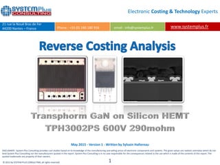
Computing and AI technologies for mobile and consumer applications 2021 - SampleYole Developpement
Penetrating everyday products will see the market for AI technologies for the consumer market reach $5.6B in 2026.
More information : https://www.i-micronews.com/products/computing-and-ai-technologies-for-mobile-and-consumer-applications-2021/
For the first time, the processor monitor is including FPGA, CPU, GPU, and APU including all the IDMs, fabless companies, and foundries in the business.
More information : https://www.i-micronews.com/products/application-processor-quarterly-market-monitor/
For the first time in its history, the automotive industry must face new industrial and technological
challenges while undergoing dramatic changes in its value chain.
More information: https://www.i-micronews.com/products/automotive-semiconductor-trends-2021/
MicroLED Displays - Market, Industry and Technology Trends 2021Yole Developpement
Strong momentum for MicroLED with progress on all fronts. Cost is the biggest challenge, but Apple and Samsung are carving paths toward the consumer.
More information; https://www.i-micronews.com/products/microled-displays-market-industry-and-technology-trends-2021/
System-in-Package Technology and Market Trends 2021 - SampleYole Developpement
Through enabling design and supply chain agility, SiP will reach $19B by 2026, with IDMs, OSATs, and foundries taking advantage of it.
More information : https://www.i-micronews.com/products/system-in-package-technology-and-market-trends-2021/
Industrial, consumer, and automotive applications are driving the adoption of neuromorphic computing and sensing technologies. The first products are now hitting the market.
More information: https://www.i-micronews.com/products/neuromorphic-computing-and-sensing-2021/
Beyond communication, silicon photonics is penetrating consumer and automotive – heading to $1.1B in 2026.
More information: https://www.i-micronews.com/products/silicon-photonics-2021/
Semiconductor technologies will enable increased mobility and communication for the soldier of the future. This market will reach $17.5B in 2030+.
More information: https://www.i-micronews.com/products/future-soldier-technologies-2021/
Intel Foveros and TSMC 3D SoIC are competing head-to-head for high-end packaging – How will Samsung react ?More information here : https://www.i-micronews.com/products/high-end-performance-packaging-3d-2-5d-integration-2020/
5G’s Impact on RF Front-End and Connectivity for Cellphones 2020Yole Developpement
An intensifying US-China competition for RF technology supremacy.
More information on: https://www.i-micronews.com/products/5gs-impact-on-rf-front-end-and-connectivity-for-cellphones-2020/
In the ultrasound module market, CMUT and PMUT are growing two times faster in medical and consumer applications.
More information: https://www.i-micronews.com/products/ultrasound-sensing-technologies-2020/
The entrance of Chinese players and the rise of new technical solutions are poised to trigger profound changes in the memory business.
More information on: https://www.i-micronews.com/products/status-of-the-memory-industry-2020/
GaAs Wafer and Epiwafer Market: RF, Photonics, LED, Display and PV Applicatio...Yole Developpement
Photonics applications boost the GaAs wafer and epiwafer market with double digit growth.
Learn more about the report here: https://www.i-micronews.com/products/gaas-wafer-and-epiwafer-market-rf-photonics-led-display-and-pv-applications-2020/
Status of the Radar Industry: Players, Applications and Technology Trends 2020Yole Developpement
Worth more than $20B in 2019, the radar industry is experiencing a major transformation prior to entering the commercial era.
Learn more about the report here: https://www.i-micronews.com/products/status-of-the-radar-industry-players-applications-and-technology-trends-2020/
GaN RF Market: Applications, Players, Technology and Substrates 2020Yole Developpement
Driven by military applications and 5G telecom infrastructure, the GaN RF market continues growing.
Learn more about the report here: https://www.i-micronews.com/products/gan-rf-market-applications-players-technology-and-substrates-2020/
Pressure, inertial, MEMS ultrasound, microfluidic chips and other sensors are driving the growth of the life sciences and healthcare market.
More information: https://www.i-micronews.com/products/biomems-market-and-technology-2020/
Market will more than double by 2025 driven by heavy investments in data centers.
More information: https://www.i-micronews.com/products/optical-transceivers-for-datacom-telecom-2020/
COVID-19 is shaking up the diagnostics industry and will have both short- and long-term impact.
More information: https://www.i-micronews.com/products/point-of-need-2020-including-pcr-based-testing/
Pluggable transceivers in high volume production. Co-packaged optics in line of sight.
More information on: https://www.i-micronews.com/products/silicon-photonics-2020/
Connector Corner: Automate dynamic content and events by pushing a buttonDianaGray10
Here is something new! In our next Connector Corner webinar, we will demonstrate how you can use a single workflow to:
Create a campaign using Mailchimp with merge tags/fields
Send an interactive Slack channel message (using buttons)
Have the message received by managers and peers along with a test email for review
But there’s more:
In a second workflow supporting the same use case, you’ll see:
Your campaign sent to target colleagues for approval
If the “Approve” button is clicked, a Jira/Zendesk ticket is created for the marketing design team
But—if the “Reject” button is pushed, colleagues will be alerted via Slack message
Join us to learn more about this new, human-in-the-loop capability, brought to you by Integration Service connectors.
And...
Speakers:
Akshay Agnihotri, Product Manager
Charlie Greenberg, Host
Transcript: Selling digital books in 2024: Insights from industry leaders - T...BookNet Canada
The publishing industry has been selling digital audiobooks and ebooks for over a decade and has found its groove. What’s changed? What has stayed the same? Where do we go from here? Join a group of leading sales peers from across the industry for a conversation about the lessons learned since the popularization of digital books, best practices, digital book supply chain management, and more.
Link to video recording: https://bnctechforum.ca/sessions/selling-digital-books-in-2024-insights-from-industry-leaders/
Presented by BookNet Canada on May 28, 2024, with support from the Department of Canadian Heritage.
State of ICS and IoT Cyber Threat Landscape Report 2024 previewPrayukth K V
The IoT and OT threat landscape report has been prepared by the Threat Research Team at Sectrio using data from Sectrio, cyber threat intelligence farming facilities spread across over 85 cities around the world. In addition, Sectrio also runs AI-based advanced threat and payload engagement facilities that serve as sinks to attract and engage sophisticated threat actors, and newer malware including new variants and latent threats that are at an earlier stage of development.
The latest edition of the OT/ICS and IoT security Threat Landscape Report 2024 also covers:
State of global ICS asset and network exposure
Sectoral targets and attacks as well as the cost of ransom
Global APT activity, AI usage, actor and tactic profiles, and implications
Rise in volumes of AI-powered cyberattacks
Major cyber events in 2024
Malware and malicious payload trends
Cyberattack types and targets
Vulnerability exploit attempts on CVEs
Attacks on counties – USA
Expansion of bot farms – how, where, and why
In-depth analysis of the cyber threat landscape across North America, South America, Europe, APAC, and the Middle East
Why are attacks on smart factories rising?
Cyber risk predictions
Axis of attacks – Europe
Systemic attacks in the Middle East
Download the full report from here:
https://sectrio.com/resources/ot-threat-landscape-reports/sectrio-releases-ot-ics-and-iot-security-threat-landscape-report-2024/
Encryption in Microsoft 365 - ExpertsLive Netherlands 2024Albert Hoitingh
In this session I delve into the encryption technology used in Microsoft 365 and Microsoft Purview. Including the concepts of Customer Key and Double Key Encryption.
Smart TV Buyer Insights Survey 2024 by 91mobiles.pdf91mobiles
91mobiles recently conducted a Smart TV Buyer Insights Survey in which we asked over 3,000 respondents about the TV they own, aspects they look at on a new TV, and their TV buying preferences.
LF Energy Webinar: Electrical Grid Modelling and Simulation Through PowSyBl -...DanBrown980551
Do you want to learn how to model and simulate an electrical network from scratch in under an hour?
Then welcome to this PowSyBl workshop, hosted by Rte, the French Transmission System Operator (TSO)!
During the webinar, you will discover the PowSyBl ecosystem as well as handle and study an electrical network through an interactive Python notebook.
PowSyBl is an open source project hosted by LF Energy, which offers a comprehensive set of features for electrical grid modelling and simulation. Among other advanced features, PowSyBl provides:
- A fully editable and extendable library for grid component modelling;
- Visualization tools to display your network;
- Grid simulation tools, such as power flows, security analyses (with or without remedial actions) and sensitivity analyses;
The framework is mostly written in Java, with a Python binding so that Python developers can access PowSyBl functionalities as well.
What you will learn during the webinar:
- For beginners: discover PowSyBl's functionalities through a quick general presentation and the notebook, without needing any expert coding skills;
- For advanced developers: master the skills to efficiently apply PowSyBl functionalities to your real-world scenarios.
Securing your Kubernetes cluster_ a step-by-step guide to success !KatiaHIMEUR1
Today, after several years of existence, an extremely active community and an ultra-dynamic ecosystem, Kubernetes has established itself as the de facto standard in container orchestration. Thanks to a wide range of managed services, it has never been so easy to set up a ready-to-use Kubernetes cluster.
However, this ease of use means that the subject of security in Kubernetes is often left for later, or even neglected. This exposes companies to significant risks.
In this talk, I'll show you step-by-step how to secure your Kubernetes cluster for greater peace of mind and reliability.
DevOps and Testing slides at DASA ConnectKari Kakkonen
My and Rik Marselis slides at 30.5.2024 DASA Connect conference. We discuss about what is testing, then what is agile testing and finally what is Testing in DevOps. Finally we had lovely workshop with the participants trying to find out different ways to think about quality and testing in different parts of the DevOps infinity loop.
Essentials of Automations: Optimizing FME Workflows with ParametersSafe Software
Are you looking to streamline your workflows and boost your projects’ efficiency? Do you find yourself searching for ways to add flexibility and control over your FME workflows? If so, you’re in the right place.
Join us for an insightful dive into the world of FME parameters, a critical element in optimizing workflow efficiency. This webinar marks the beginning of our three-part “Essentials of Automation” series. This first webinar is designed to equip you with the knowledge and skills to utilize parameters effectively: enhancing the flexibility, maintainability, and user control of your FME projects.
Here’s what you’ll gain:
- Essentials of FME Parameters: Understand the pivotal role of parameters, including Reader/Writer, Transformer, User, and FME Flow categories. Discover how they are the key to unlocking automation and optimization within your workflows.
- Practical Applications in FME Form: Delve into key user parameter types including choice, connections, and file URLs. Allow users to control how a workflow runs, making your workflows more reusable. Learn to import values and deliver the best user experience for your workflows while enhancing accuracy.
- Optimization Strategies in FME Flow: Explore the creation and strategic deployment of parameters in FME Flow, including the use of deployment and geometry parameters, to maximize workflow efficiency.
- Pro Tips for Success: Gain insights on parameterizing connections and leveraging new features like Conditional Visibility for clarity and simplicity.
We’ll wrap up with a glimpse into future webinars, followed by a Q&A session to address your specific questions surrounding this topic.
Don’t miss this opportunity to elevate your FME expertise and drive your projects to new heights of efficiency.
Epistemic Interaction - tuning interfaces to provide information for AI supportAlan Dix
Paper presented at SYNERGY workshop at AVI 2024, Genoa, Italy. 3rd June 2024
https://alandix.com/academic/papers/synergy2024-epistemic/
As machine learning integrates deeper into human-computer interactions, the concept of epistemic interaction emerges, aiming to refine these interactions to enhance system adaptability. This approach encourages minor, intentional adjustments in user behaviour to enrich the data available for system learning. This paper introduces epistemic interaction within the context of human-system communication, illustrating how deliberate interaction design can improve system understanding and adaptation. Through concrete examples, we demonstrate the potential of epistemic interaction to significantly advance human-computer interaction by leveraging intuitive human communication strategies to inform system design and functionality, offering a novel pathway for enriching user-system engagements.
34. COMPLETE TEARDOWN WITH:
• Detailed photos and
identification
• SEM analysis of epitaxy
layers and transistor
structure
• Analysis of Quiet-Tab™
packaging from Transphorm
• Manufacturing process flow
• In-depth economic analysis
• Manufacturing cost
breakdown
• Selling price estimation
• Comparison with TPH3002
and GaN Systems’ GS66504B
Transphorm GaN-on-Silicon
HEMT TPH3206PS
Title: Transphorm GaN-on-Si
HEMT TPH3206PS
Pages: 120
Date: December 2016
Format: PDF & Excel file
Price: Full report: EUR 3,290
Transphorm’s TPH3206PS
transistor has a new die
design and manufacturing
process. The die contacts are
optimized on the die area to
save space, and increase
c u r r e n t d e n s i t y. T h e
transistor metal contact and
field plate structure have
Transphorm’s new die design for its TPH3206PS GaN HEMT
halves the cost per ampere compared to the previous model
also been changed from the previous version. These innovations
halve the cost per ampere compared to the previous model.
The TPH3206PS is a 600V EZ-GaN™ HEMT for high frequency
operation from Transphorm. Manufactured by Fujitsu and assembled
in a TO220 package, it features the Quiet-Tab™ scheme, which
increases switching speed.
The TPH3206PS combines a normally-on GaN-on-Silicon HEMT, which
withstands high voltages, and a standard low voltage MOSFET, which
drives high frequency, in a cascode configuration that ultimately yields
a normally-off transistor.
Based on a complete teardown analysis, the report also provides an
estimation of the production cost of the package, HEMT, MOSFET and
resistor.
The report also proposes a comparison with the GaN Systems
GS66504B 650V HEMT. This comparison highlights the huge
differences in design and manufacturing process and their impact on
device size and production cost.
35. Véronique is in charge of
structure analysis of semi-
conductors. She has a deep
knowledge in chemical &
physical technical analyses. She
previously worked for 20 years
in Atmel Nantes Laboratory.
Author (Lab):
Véronique
Le Troadec
lyses for MEMS, IC and Power
Semi-conductors. She has a
deep knowledge of Electronics
R&D and Manufacturing
environment. Elena holds a
Master in Nanotechnologies
and a PhD in Power Electronics.
Elena
Barbarini
Elena is in charge
of costing ana-
AUTHORS:
Performed by
TABLE OF CONTENTS
Overview/Introduction
Company Profile
TPH3206PS Characteristics
Physical Analysis
• Synthesis of the Physical Analysis
• Package Analysis
View and dimensions and marking
Package opening
Package cross-section
• GaN on Silicon HEMT Analysis
Dimension and marking
Details and delayering
Cross-section, SEM view
• Resistor Analysis
Dimension
Details and process
Cross- section
• Silicon MOSFET
Dimension
Details
Cross-section
Manufacturing Process Flow
• GaN HEMT Process Flow and
Fabrication Units
• Resistor Process Flow and
Fabrication Units
• MOSFET Process Flow and
Fabrication Units
• Package Process Flow
Cost Analysis
• Synthesis of the Cost Analysis
• Main Steps of Economic Analysis
• Yields Explanation
• Cost Analysis GaN HEMT
GaN HEMT wafer cost
Breakdown per process step
Back-end cost
GaN HEMT die cost
• Resistor Cost Analysis
Resistor wafer cost
Breakdown per process step
Resistor die cost
• MOSFET Cost Analysis
MOSFET wafer cost
Back-end cost
MOSFET die cost
• TPH3206PS Cost Analysis
Assessing BOM
DBC cost
TPH3206PS module cost
Estimated Manufacturer Price
Analysis
• Manufacturers ratios
• Estimated manufacturer price
Comparison with Transphorm
TPH3002PS
Comparison with GaN System
GS66504B
POWER tools
Cost simulation tool to evaluate
the cost of any POWER process
or device: from single chip to
complex structures.
POWER CoSim+ is a process-
based costing tool used to
evaluate the manufacturing cost
per wafer using your own inputs
or using the pre-defined
parameters included in the tool.
POWER Price+ is a parametric
costing tool used to evaluate
the manufacturing cost of
devices using few process
related inputs.
All these tools are on sale under
corporate licence.
ANALYSIS PERFORMED WITH OUR COSTING TOOLS POWER COSIM+ AND POWER PRICE+
Power CoSim+ Power Price+
Consulting in 2011, in order
to set up the laboratory of
System Plus Consulting. He
previously worked during 25
years in Atmel Nantes
Technological Analysis Labo-
ratory as fab support in
physical analysis, and 3 years
at Hirex Engineering in
Toulouse, in a DPA lab.
Yvon
Le Goff (Lab)
Yvon has joined
S y s t e m P l u s
36. GaN on Si HEMT vs SJ
MOSFET : Technology and
Cost Comparison
Transphorm TPH3002PS
600V GaN on Silicon
HEMT
GaN Systems
650V GaN on Silicon
HEMT
Will SJ MOSFETs still be attractive
compared to GaN devices? Latest
innovations in 600/650V power
devices…
High voltage GaN HEMT
developed for the high frequency
operation in a low-inductance
source terminal TO220 package.
650V 52mΩ enhancement mode
GaN transistor in the new AT&S
Embedded Power Die Package.
Pages: 210
Date: March 2016
Full report: EUR 4,490*
Pages: 137
Date: May 2015
Full report: EUR 3,290*
Pages: 110
Date: January 2015
Full report: EUR 2,990*
RELATED REPORTS
ANNUAL SUBSCRIPTION OFFER
You can choose to buy over 12
months a set of 3, 4, 5, 7, 10 or
15 Reverse Costing® reports.
Up to 47% discount!
More than 40 reports released each year on the following topics (considered for 2016):
• MEMS & Sensors (20 reports):
• Gyros/Accelerometers/IMU
• Oscillators/RF switches
• Pressure sensors/Gas sensors
• Power Electronics & Systems (12 reports):
• GaN and SiC devices
• Inverters & modules
• Automotive radars
• Head Up displays, Displays
Each year System Plus Consulting releases a comprehensive collection of new reverse engineering &
costing analyses in various domains.
• ICs (3 reports):
• Multimedia SoC
• Ethernet for car IC, etc.
• Imaging & LEDs (11 reports):
• Camera modules, Infrared
sensors & cameras
• LEDs
• Advanced Packaging (5 reports):
• WLP, TSV
• Embedded devices, etc.
Performed by
37. DELIVERY on receipt of payment:
By credit card:
Number: |__|__|__|__| |__|__|__|__| |__|__|__|__| |__|__|__|__|
Expiration date: |__|__|/|__|__| Card Verification Value: |__|__|__|
By bank transfer:
BANK INFO: HSBC, 1 place de la Bourse, F-69002 Lyon, France,
Bank code : 30056, Branch code : 00170
Account No : 0170 200 1565 87,
SWIFT or BIC code : CCFRFRPP,
IBAN : FR76 3005 6001 7001 7020 0156 587
Return order by:
• FAX: +33 (0)472 83 01 83
• MAIL: YOLE DEVELOPPEMENT,
75 Cours Emile Zola, F - 69100 Lyon - Villeurbanne
Contact:
• Japan: Miho - Ohtake@yole.fr
• Greater China: Mavis - Wang@yole.fr
• Asia: Takashi - Onozawa@yole.fr
• EMEA: Lizzie - Levenez@yole.fr
• North America: Steve – laferriere@yole.fr
• General: info@yole.fr
The present document is valid till November 15, 2017
SHIP TO PAYMENT
BILLING CONTACT
ABOUT YOLE DEVELOPPEMENT
Name (Mr/Ms/Dr/Pr):
......................................................................................
Job Title:
......................................................................................
Company:
......................................................................................
Address:
......................................................................................
City: State:
......................................................................................
Postcode/Zip:
......................................................................................
Country:
......................................................................................
VAT ID Number for EU members:
......................................................................................
Tel:
......................................................................................
Email:
.....................................................................................
Date:
.......................................................................................
Signature:
......................................................................................
Full Reverse Costing report: EUR 3,290*
ORDER FORM
Performed by
Distributed by
First Name: .................................................................. Last Name: ............................................................................
Email:............................................................................ Phone:.....................................................................................
About Yole Développement – www.yole.fr / www.i-micronews.com
Founded in 1998, Yole Développement (Yole) has grown to become a group of companies providing marketing, technology and strategy
consulting, media in addition to corporate finance services. With a strong focus on emerging applications using silicon and/or micro
manufacturing, Yole has expanded to include more than 50 collaborators worldwide covering MEMS, Compound Semi., LED, Image
Sensors, Optoelectronics, Microfluidics & Medical, Photovoltaics, Advanced Packaging, Manufacturing and Power Electronics. We
support industrial companies, investors and R&D organizations worldwide to help them understand markets and follow technology trends
to develop their business.
CONSULTING
• Market data & research,
marketing analysis
• Technology analysis
• Reverse engineering & costing
services
• Strategy consulting
• Patent analysis
FINANCIAL SERVICES
• Mergers & Acquisitions
• Due diligence
• Fundraising
More information on
www.yolefinance.com
REPORTS
• Collection of technology &
market reports
• Manufacturing cost
simulation tools
• Component reverse
engineering & costing analysis
• Patent investigation
MEDIA & EVENTS
• i-Micronews.com, online disruptive
technologies website
• @Micronews, weekly e-newsletter
• Technology Magazines dedicated to
MEMS, Advanced Packaging, LED and
Power Electronics
• Communication & webcasts services
• Events: Yole Seminars, Market Briefings
Please process my order for “Transphorm TPH3002PS” Reverse Costing Report
*For price in dollars please use the day’s exchange rate. All reports are delivered electronically in pdf format. For French customer, add 20 % for VAT.
38. Performed by
TERMS AND CONDITIONS OF SALES
. Definitions: “Acceptance”: Action by which the Buyer accepts the terms and conditions of sale in their entirety. It is done by signing the purchase order which mentions “I hereby accept Yole’s Terms and Conditions of
Sale”.
“Buyer”: Any business user (i.e. any person acting in the course of its business activities, for its business needs) entering into the following general conditions to the exclusion of consumers acting in their personal
interests.
“Contracting Parties” or “Parties”: The Seller on the one hand and the Buyer on the other hand.
“Intellectual Property Rights” (“IPR”) means any rights held by the Seller in its Products, including any patents, trademarks, registered models, designs, copyrights, inventions, commercial secrets and know-how, technical
information, company or trading names and any other intellectual property rights or similar in any part of the world, notwithstanding the fact that they have been registered or not and including any pending registration of
one of the above mentioned rights.
“License”: For the reports and databases, 3 different licenses are proposed. The buyer has to choose one license:
• One user license: one person at the company can use the report.
• Multi-user license: the report can be used by unlimited users within the company. Subsidiaries and Joint-Ventures are not included.
• Corporate license: purchased under “Annual Subscription” program, the report can be used by unlimited users within the company. Joint-Ventures are not included.
“Products”: Depending on the purchase order, reports or database on MEMS, CSC, Optics/MOEMS, Nano, bio… to be bought either on a unit basis or as an annual subscription. (i.e. subscription for a period of 12
calendar months). The annual subscription to a package (i.e. a global discount based on the number of reports that the Buyer orders or accesses via the service, a global search service on line on I-micronews and a
consulting approach), is defined in the order. Reports are established in PowerPoint and delivered on a PDF format and the database may include Excel files.
“Seller”: Based in Lyon (France headquarters), Yole Développement is a market research and business development consultancy company, facilitating market access for advanced technology industrial projects. With
more than 20 market analysts, Yole works worldwide with the key industrial companies, R&D institutes and investors to help them understand the markets and technology trends.
1. Scope
1.1 The Contracting Parties undertake to observe the following general conditions when agreed by the Buyer and the Seller. ANY ADDITIONAL, DIFFERENT, OR CONFLICTING TERMS AND CONDITIONS IN ANY
OTHER DOCUMENTS ISSUED BY THE BUYER AT ANY TIME ARE HEREBY OBJECTED TO BY THE SELLER, SHALL BE WHOLLY INAPPLICABLE TO ANY SALE MADE HEREUNDER AND SHALL NOT BE
BINDING IN ANY WAY ON THE SELLER.
1.2 This agreement becomes valid and enforceable between the Contracting Parties after clear and non-equivocal consent by any duly authorized person representing the Buyer. For these purposes, the Buyer accepts
these conditions of sales when signing the purchase order which mentions “I hereby accept Yole’s Terms and Conditions of Sale”. This results in acceptance by the Buyer.
1.3 Orders are deemed to be accepted only upon written acceptance and confirmation by the Seller, within [7 days] from the date of order, to be sent either by email or to the Buyer’s address. In the absence of any
confirmation in writing, orders shall be deemed to have been accepted.
2. Mailing of the Products
2.1 Products are sent by email to the Buyer:
- within [1] month from the order for Products already released; or
- within a reasonable time for Products ordered prior to their effective release. In this case, the Seller shall use its best endeavours to inform the Buyer of an indicative release date and the evolution of the work in
progress.
2.2 Some weeks prior to the release date the Seller can propose a pre-release discount to the Buyer
The Seller shall by no means be responsible for any delay in respect of article 2.2 above, and including incases where a new event or access to new contradictory information would require for the analyst extra time to
compute or compare the data in order to enable the Seller to deliver a high quality Products.
2.3 The mailing of the Product will occur only upon payment by the Buyer, in accordance with the conditions contained in article 3.
2.4. The mailing is operated through electronic means either by email via the sales department or automatically online via an email/password. If the Product’s electronic delivery format is defective, the Seller undertakes to
replace it at no charge to the Buyer provided that it is informed of the defective formatting within 90 days from the date of the original download or receipt of the Product.
2.5 The person receiving the Products on behalf of the Buyer shall immediately verify the quality of the Products and their conformity to the order. Any claim for apparent defects or for non-conformity shall be sent in
writing to the Seller within 8 days of receipt of the Products. For this purpose, the Buyer agrees to produce sufficient evidence of such defects. .
2.6 No return of Products shall be accepted without prior information to the Seller, even in case of delayed delivery. Any Product returned to the Seller without providing prior information to the Seller as required under
article 2.5 shall remain at the Buyer’s risk.
3. Price, invoicing and payment
3.1 Prices are given in the orders corresponding to each Product sold on a unit basis or corresponding to annual subscriptions. They are expressed to be inclusive of all taxes. The prices may be reevaluated from time
to time. The effective price is deemed to be the one applicable at the time of the order.
3.2 Yole may offer a pre release discount for the companies willing to acquire in the future the specific report and agreeing on the fact that the report may be release later than the anticipated release date. In exchange
to this uncertainty, the company will get a discount that can vary from 15% to 10%.
3.3 Payments due by the Buyer shall be sent by cheque payable to Yole Développement, credit card or by electronic transfer to the following account:
HSBC, 1 place de la Bourse 69002 Lyon France
Bank code: 30056
Branch code: 00170
Account n°: 0170 200 1565 87
BIC or SWIFT code: CCFRFRPP
IBAN: FR76 3005 6001 7001 7020 0156 587
To ensure the payments, the Seller reserves the right to request down payments from the Buyer. In this case, the need of down payments will be mentioned on the order.
3.4 Payment is due by the Buyer to the Seller within 30 days from invoice date, except in the case of a particular written agreement. If the Buyer fails to pay within this time and fails to contact the Seller, the latter shall be
entitled to invoice interest in arrears based on the annual rate Refi of the «BCE» + 7 points, in accordance with article L. 441-6 of the French Commercial Code. Our publications (report, database, tool...) are delivered
only after reception of the payment.
3.5 In the event of termination of the contract, or of misconduct, during the contract, the Seller will have the right to invoice at the stage in progress, and to take legal action for damages.
4. Liabilities
4.1 The Buyer or any other individual or legal person acting on its behalf, being a business user buying the Products for its business activities, shall be solely responsible for choosing the Products and for the use and
interpretations he makes of the documents it purchases, of the results he obtains, and of the advice and acts it deduces thereof.
4.2 The Seller shall only be liable for (i) direct and (ii) foreseeable pecuniary loss, caused by the Products or arising from a material breach of this agreement
4.3 In no event shall the Seller be liable for:
a) damages of any kind, including without limitation, incidental or consequential damages (including, but not limited to, damages for loss of profits, business interruption and loss of programs or information) arising out of
the use of or inability to use the Seller’s website or the Products, or any information provided on the website, or in the Products;
b) any claim attributable to errors, omissions or other inaccuracies in the Product or interpretations thereof.
4.4All the information contained in the Products has been obtained from sources believed to be reliable. The Seller does not warrant the accuracy, completeness adequacy or reliability of such information, which cannot
be guaranteed to be free from errors.
4.5 All the Products that the Seller sells may, upon prior notice to the Buyer from time to time be modified by or substituted with similar Products meeting the needs of the Buyer. This modification shall not lead to the
liability of the Seller, provided that the Seller ensures the substituted Product is similar to the Product initially ordered.
4.6 In the case where, after inspection, it is acknowledged that the Products contain defects, the Seller undertakes to replace the defective products as far as the supplies allow and without indemnities or compensation of
any kind for labor costs, delays, loss caused or any other reason. The replacement is guaranteed for a maximum of two months starting from the delivery date. Any replacement is excluded for any event as set out in
article 5 below.
4.7 The deadlines that the Seller is asked to state for the mailing of the Products are given for information only and are not guaranteed. If such deadlines are not met, it shall not lead to any damages or cancellation of the
orders, except for non acceptable delays exceeding [4] months from the stated deadline, without information from the Seller. In such case only, the Buyer shall be entitled to ask for a reimbursement of its first down
payment to the exclusion of any further damages.
4.8 The Seller does not make any warranties, express or implied, including, without limitation, those of sale ability and fitness for a particular purpose, with respect to the Products. Although the Seller shall take
reasonable steps to screen Products for infection of viruses, worms, Trojan horses or other codes containing contaminating or destructive properties before making the Products available, the Seller cannot guarantee that
any Product will be free from infection.
5. Force majeure
The Seller shall not be liable for any delay in performance directly or indirectly caused by or resulting from acts of nature, fire, flood, accident, riot, war, government intervention, embargoes, strikes, labor difficulties,
equipment failure, late deliveries by suppliers or other difficulties which are beyond the control, and not the fault of the Seller.
6. Protection of the Seller’s IPR
6.1 All the IPR attached to the Products are and remain the property of the Seller and are protected under French and international copyright law and conventions.
6.2 The Buyer agreed not to disclose, copy, reproduce, redistribute, resell or publish the Product, or any part of it to any other party other than employees of its company. The Buyer shall have the right to use the
Products solely for its own internal information purposes. In particular, the Buyer shall therefore not use the Product for purposes such as:
- Information storage and retrieval systems;
- Recordings and re-transmittals over any network (including any local area network);
- Use in any timesharing, service bureau, bulletin board or similar arrangement or public display;
- Posting any Product to any other online service (including bulletin boards or the Internet);
- Licensing, leasing, selling, offering for sale or assigning the Product.
6.3 The Buyer shall be solely responsible towards the Seller of all infringements of this obligation, whether this infringement comes from its employees or any person to whom the Buyer has sent the Products and shall
personally take care of any related proceedings, and the Buyer shall bear related financial consequences in their entirety.
6.4 The Buyer shall define within its company point of contact for the needs of the contract. This person will be the recipient of each new report in PDF format. This person shall also be responsible for respect of the
copyrights and will guaranty that the Products are not disseminated out of the company.
6.5 In the context of annual subscriptions, the person of contact shall decide who within the Buyer, shall be entitled to access on line the reports on I-micronews.com. In this respect, the Seller will give the Buyer a
maximum of 10 password, unless the multiple sites organization of the Buyer requires more passwords. The Seller reserves the right to check from time to time the correct use of this password.
6.6 In the case of a multisite, multi license, only the employee of the buyer can access the report or the employee of the companies in which the buyer have 100% shares. As a matter of fact the investor of a company,
the joint venture done with a third party etc..cannot access the report and should pay a full license price.
7. Termination
7.1 If the Buyer cancels the order in whole or in part or postpones the date of mailing, the Buyer shall indemnify the Seller for the entire costs that have been incurred as at the date of notification by the Buyer of such
delay or cancellation. This may also apply for any other direct or indirect consequential loss that may be borne by the Seller, following this decision.
7.2 In the event of breach by one Party under these conditions or the order, the non-breaching Party may send a notification to the other by recorded delivery letter upon which, after a period of thirty (30) days without
solving the problem, the non-breaching Party shall be entitled to terminate all the pending orders, without being liable for any compensation.
8. Miscellaneous
All the provisions of these Terms and Conditions are for the benefit of the Seller itself, but also for its licensors, employees and agents. Each of them is entitled to assert and enforce those provisions against the Buyer.
Any notices under these Terms and Conditions shall be given in writing. They shall be effective upon receipt by the other Party.
The Seller may, from time to time, update these Terms and Conditions and the Buyer, is deemed to have accepted the latest version of these terms and conditions, provided they have been communicated to him in due
time.
9. Governing law and jurisdiction
9.1 Any dispute arising out or linked to these Terms and Conditions or to any contract (orders) entered into in application of these Terms and Conditions shall be settled by the French Commercial Courts of Lyon, which
shall have exclusive jurisdiction upon such issues.
9.2 French law shall govern the relation between the Buyer and the Seller, in accordance with these Terms and Conditions.