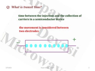
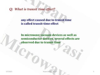
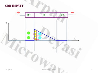
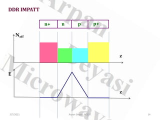
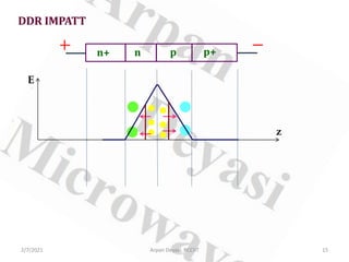
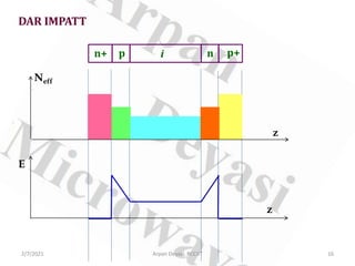
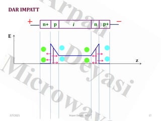
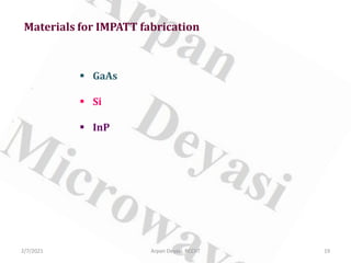
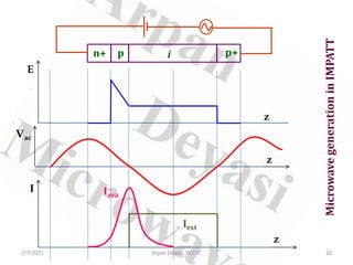
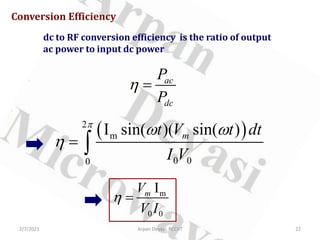
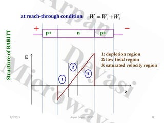
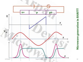
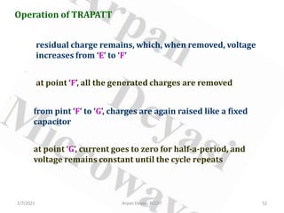
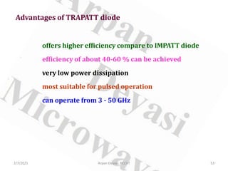
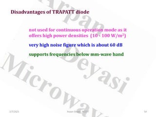
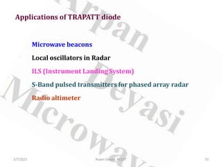
Transit-Time Device
Course coordinator: Arpan Deyasi
2/7/2021 1
Arpan Deyasi, RCCIIT
Q: What is transit time?
time between the injection and the collection of
carriers in a semiconductor device
the movement is considered between
two electrodes
2/7/2021 2
Arpan Deyasi, RCCIIT
Q: What is transit time effect?
any effect caused due to transit time
is called transit-time effect
In microwave vacuum devices as well as
semiconductor devices, several effects are
observed due to transit time
2/7/2021 3
Arpan Deyasi, RCCIIT
Q: What is transit time device?
transit time causes a change of phase between
voltage and current in a semiconductor device
Q: How the effect becomes significant?
If the effect causes 180° phase shift between voltage
and current, then it exhibits negative resistance
2/7/2021 4
Arpan Deyasi, RCCIIT
Avalanche Transit Time Device
If both avalanche and transit time effect together
cause the negative resistance, then the device is
called Avalanche Transit Time Device
2/7/2021 5
Arpan Deyasi, RCCIIT
Types of ATT
IMPATT: IMPact ionization Avalanche Transit Time
TRAPATT: TRApped Plasma Avalanche Triggered Transit
BARITT: BARrier Injection Transit Time
QWITT: Quantum Well Injection Transit Time
2/7/2021 6
Arpan Deyasi, RCCIIT
IMPATT
2/7/2021 7
Arpan Deyasi, RCCIIT
Features of IMPATT
Operating region: 16-300 GHz ---- specifically operates
at window Frequencies (16, 34, 94, 140, 220, 301 GHz)
Generates high level of phase noise due to avalanche
Process (~40 dB)
High power capability
2/7/2021 8
Arpan Deyasi, RCCIIT
Classification of IMPATT
SDR: Single Drift Region
DDR: Double Drift Region
DAR: Double Avalanche Region
2/7/2021 9
Arpan Deyasi, RCCIIT
SDR IMPATT: Read type
n+ p i p+
E
z
z
Neff
2/7/2021 10
Arpan Deyasi, RCCIIT
SDR IMPATT: Read type
n+ p i p+
E
z
2/7/2021 11
Arpan Deyasi, RCCIIT
SDR IMPATT
n+ p p+
E
z
z
Neff
2/7/2021 12
Arpan Deyasi, RCCIIT
SDR IMPATT
n+ p p+
E
z
2/7/2021 13
Arpan Deyasi, RCCIIT
DDR IMPATT
E
z
z
Neff
n+ n p p+
2/7/2021 14
Arpan Deyasi, RCCIIT
DDR IMPATT
E
z
n+ n p p+
2/7/2021 15
Arpan Deyasi, RCCIIT
DAR IMPATT
E
z
z
Neff
n+ p i p+
n
2/7/2021 16
Arpan Deyasi, RCCIIT
DAR IMPATT
E
z
n+ p i p+
n
2/7/2021 17
Arpan Deyasi, RCCIIT
carriers are drifted in respective sides after generation due
to applied reverse bias
Carrier flow in IMPATT
Avalanche multiplication always takes place at the junction
of highly doped and moderately doped region
2/7/2021 18
Arpan Deyasi, RCCIIT
Materials for IMPATT fabrication
 GaAs
 Si
 InP
2/7/2021 19
Arpan Deyasi, RCCIIT
Microwave
generation
in
IMPATT
n+ p i p+
E
z
Vac
z
z
I Iava
Iext
2/7/2021 20
Arpan Deyasi, RCCIIT
Microwave generation in IMPATT
external current due to moving carriers is delayed by 90°
relative to pulsed current
pulsed current is delayed by 90° relative to ac voltage
phase difference becomes 180° between external
current and applied ac voltage
negative conductance occurs which leads to
microwave oscillation
2/7/2021 21
Arpan Deyasi, RCCIIT
Conversion Efficiency
dc to RF conversion efficiency is the ratio of output
ac power to input dc power
ac
dc
P
P
η =
( )
2
m
0 0
0
I sin( )( sin( )
m
t V t dt
I V
π
ω ω
η = ∫
m
0 0
I
m
V
V I
η =
2/7/2021 22
Arpan Deyasi, RCCIIT
Power output of IMPATT
at low ‘f’, power output is inversely proportional
to frequency
at high ‘f’, power output is inversely proportional
to square of frequency
2/7/2021 23
Arpan Deyasi, RCCIIT
2/7/2021 Arpan Deyasi, RCCIIT 24
Advantages of IMPATT diode
Operates from 3 - 100 GHz frequency range
high power capabilities compare to other microwave
diodes
output is more reliable compare to other microwave
diodes
acts as a narrow band device when used as amplifier
can be used as excellent microwave generators
can produce carrier signal for microwave transmission
system
2/7/2021 Arpan Deyasi, RCCIIT 25
Disadvantages of IMPATT diode
has high noise figure due to avalanche process & higher
operating current
shot noise is generated in the device due to high
operating current
noise figure of IMPATT is about 35 dB
produces spurious noise (AM and FM) with higher levels
compare to klystron and Gunn diodes
tuning range of IMPATT diode is not as good as Gunn
diode
offers lower efficiency compare to TRAPATT diode
Application of IMPATT
Negative resistance parametric amplifier
Microwave source
CW Doppler RADAR transmitter
2/7/2021 26
Arpan Deyasi, RCCIIT
BARITT
2/7/2021 27
Arpan Deyasi, RCCIIT
Features of BARITT
generates low noise microwave power at lower
microwave frequency (up to X-band)
large transit time
uses thermionic emission rather avalanche process
2/7/2021 28
Arpan Deyasi, RCCIIT
Structure
of
BARITT
W1 W2
Neff
z
z
E
p+ n p+
2/7/2021 29
Arpan Deyasi, RCCIIT
Widths of BARITT
1
1
2
( )
D bi
W
qN V V
ε
=
−
2
2
2
( )
D bi
W
qN V V
ε
=
−
for forward bias junction
for reverse bias junction
2/7/2021 30
Arpan Deyasi, RCCIIT
Structure
of
BARITT
at reach-through condition 1 2
W W W
= +
p+ n p+
E
z
1
2
3
1: depletion region
2: low field region
3: saturated velocity region
2/7/2021 31
Arpan Deyasi, RCCIIT
Microwave
generation
in
BARITT
n+ p p+
E
z
Vac
z
z
2/7/2021 32
Arpan Deyasi, RCCIIT
2/7/2021 Arpan Deyasi, RCCIIT 33
Microwave generation in BARITT
Carriers are thermionically injected over the barrier
in presence of ac field
Voltage reaches the maximum
Peak current is delayed w.r.t ac voltage by T/4
External current induced in the circuit when the charge
bunch travels through the reverse-biased depletion layer
takes ¾ of the time-period to reach the negative
terminal
3
2
2
d
f
π
π τ =
3
4 d
f
τ
=
3
4
s
v
f
w
=
2/7/2021 34
Arpan Deyasi, RCCIIT
Frequency of BARITT
Advantages of BARITT diode
less noisy due to thermionic emissions
offers noise figure of about 15 dB
2/7/2021 35
Arpan Deyasi, RCCIIT
Disadvantages of BARITT diode
relatively narrower bandwidth
lower power handling capability
efficiency of the BARITT diode decreases with
increase in the frequency
2/7/2021 36
Arpan Deyasi, RCCIIT
Applications of BARITT diode
 Mixer
 Large signal Oscillator
 Small signal amplifier
2/7/2021 37
Arpan Deyasi, RCCIIT
TRAPATT
2/7/2021 38
Arpan Deyasi, RCCIIT
2/7/2021 Arpan Deyasi, RCCIIT 39
Features of TRAPATT
produces high microwave power with very high dc-to-RF
conversion efficiency (40-60%)
operated under pulsed condition
characterized by lower oscillation frequency
Structure of TRAPATT
p+ n n+
E
z
z
Neff
2/7/2021 40
Arpan Deyasi, RCCIIT
2/7/2021 Arpan Deyasi, RCCIIT 41
Trapping
of
plasma
plasma of very high density is created by
avalanche electric field
this makes collapse of field owing to sharp
increase of conductivity in the region
carriers drift very slowly, i.e., plasma is trapped
2/7/2021 Arpan Deyasi, RCCIIT 42
Propagation of avalanche shock-front
τ1
W
z
E
p+ n n+
2/7/2021 Arpan Deyasi, RCCIIT 43
Propagation of avalanche shock-front
W
z
E
τ2
p+ n n+
2/7/2021 Arpan Deyasi, RCCIIT 44
Propagation of avalanche shock-front
W
z
E
p+ n n+
τ3
2/7/2021 Arpan Deyasi, RCCIIT 45
Propagation of avalanche shock-front
W
z
E
p+ n n+
τ4
. D
D qN
∇ =
 
D
E
qN
z
ε
∆
=
∆
D
qN
E
z ε
∆
=
∆
2/7/2021 46
Arpan Deyasi, RCCIIT
Velocity of Avalanche Shock-Front
Field rises in the carrier free drift region during shock
Front propagation
z
E I
v
t ε
∆
= =
∆
Shock-front velocity
2/7/2021 47
Arpan Deyasi, RCCIIT
Velocity of Avalanche Shock-Front
( )
( )
E
z t
E
t
z
∆
∆ ∆
=
∆
∆
∆
( )
D
I
z
qN
t
ε
ε
∆
=
∆  
 
 
z
D
I
v
qN
=
2/7/2021 48
Arpan Deyasi, RCCIIT
Velocity
of
Avalanche
Shock-Front
2/7/2021 Arpan Deyasi, RCCIIT 49
Operation of TRAPATT
A
B
C
D
E
F
G
A
τ
t
0.5τ
charging
plasma formation
residual extraction
plasma extraction
charging
voltage
/
current
2/7/2021 Arpan Deyasi, RCCIIT 50
Operation of TRAPATT
at point ‘A’, electric field is uniform throughout the sample
and its magnitude is large but less than the value required
for avalanche breakdown
at ‘A’, diode current is turned ON
diode behaves like a linear capacitor and reaches at
point ‘B’ owing to charging
2/7/2021 Arpan Deyasi, RCCIIT 51
Operation of TRAPATT
after generation of sufficient carriers, electric field is
depressed throughout the depletion region, causing
voltage to decrease; shown from ‘B’ to ‘C’
as few carriers are drifted out, field is further depressed
and traps the remaining plasma, so voltage reaches at
point ‘D’
at point ‘E’, plasma is removed
2/7/2021 Arpan Deyasi, RCCIIT 52
Operation of TRAPATT
residual charge remains, which, when removed, voltage
increases from ‘E’ to ‘F’
at point ‘F’, all the generated charges are removed
from pint ‘F’ to ‘G’, charges are again raised like a fixed
capacitor
at point ‘G’, current goes to zero for half-a-period, and
voltage remains constant until the cycle repeats
2/7/2021 53
Arpan Deyasi, RCCIIT
Advantages of TRAPATT diode
offers higher efficiency compare to IMPATT diode
efficiency of about 40-60 % can be achieved
very low power dissipation
most suitable for pulsed operation
can operate from 3 - 50 GHz
2/7/2021 54
Arpan Deyasi, RCCIIT
Disadvantages of TRAPATT diode
not used for continuous operation mode as it
offers high power densities (10 - 100 W/m2)
very high noise figure which is about 60 dB
supports frequencies below mm-wave band
2/7/2021 55
Arpan Deyasi, RCCIIT
Applications of TRAPATT diode
Microwave beacons
Local oscillators in Radar
ILS (Instrument Landing System)
S-Band pulsed transmitters for phased array radar
Radio altimeter

Transit time device

  • 1.
    Transit-Time Device Course coordinator:Arpan Deyasi 2/7/2021 1 Arpan Deyasi, RCCIIT
  • 2.
    Q: What istransit time? time between the injection and the collection of carriers in a semiconductor device the movement is considered between two electrodes 2/7/2021 2 Arpan Deyasi, RCCIIT
  • 3.
    Q: What istransit time effect? any effect caused due to transit time is called transit-time effect In microwave vacuum devices as well as semiconductor devices, several effects are observed due to transit time 2/7/2021 3 Arpan Deyasi, RCCIIT
  • 4.
    Q: What istransit time device? transit time causes a change of phase between voltage and current in a semiconductor device Q: How the effect becomes significant? If the effect causes 180° phase shift between voltage and current, then it exhibits negative resistance 2/7/2021 4 Arpan Deyasi, RCCIIT
  • 5.
    Avalanche Transit TimeDevice If both avalanche and transit time effect together cause the negative resistance, then the device is called Avalanche Transit Time Device 2/7/2021 5 Arpan Deyasi, RCCIIT
  • 6.
    Types of ATT IMPATT:IMPact ionization Avalanche Transit Time TRAPATT: TRApped Plasma Avalanche Triggered Transit BARITT: BARrier Injection Transit Time QWITT: Quantum Well Injection Transit Time 2/7/2021 6 Arpan Deyasi, RCCIIT
  • 7.
  • 8.
    Features of IMPATT Operatingregion: 16-300 GHz ---- specifically operates at window Frequencies (16, 34, 94, 140, 220, 301 GHz) Generates high level of phase noise due to avalanche Process (~40 dB) High power capability 2/7/2021 8 Arpan Deyasi, RCCIIT
  • 9.
    Classification of IMPATT SDR:Single Drift Region DDR: Double Drift Region DAR: Double Avalanche Region 2/7/2021 9 Arpan Deyasi, RCCIIT
  • 10.
    SDR IMPATT: Readtype n+ p i p+ E z z Neff 2/7/2021 10 Arpan Deyasi, RCCIIT
  • 11.
    SDR IMPATT: Readtype n+ p i p+ E z 2/7/2021 11 Arpan Deyasi, RCCIIT
  • 12.
    SDR IMPATT n+ pp+ E z z Neff 2/7/2021 12 Arpan Deyasi, RCCIIT
  • 13.
    SDR IMPATT n+ pp+ E z 2/7/2021 13 Arpan Deyasi, RCCIIT
  • 14.
    DDR IMPATT E z z Neff n+ np p+ 2/7/2021 14 Arpan Deyasi, RCCIIT
  • 15.
    DDR IMPATT E z n+ np p+ 2/7/2021 15 Arpan Deyasi, RCCIIT
  • 16.
    DAR IMPATT E z z Neff n+ pi p+ n 2/7/2021 16 Arpan Deyasi, RCCIIT
  • 17.
    DAR IMPATT E z n+ pi p+ n 2/7/2021 17 Arpan Deyasi, RCCIIT
  • 18.
    carriers are driftedin respective sides after generation due to applied reverse bias Carrier flow in IMPATT Avalanche multiplication always takes place at the junction of highly doped and moderately doped region 2/7/2021 18 Arpan Deyasi, RCCIIT
  • 19.
    Materials for IMPATTfabrication  GaAs  Si  InP 2/7/2021 19 Arpan Deyasi, RCCIIT
  • 20.
    Microwave generation in IMPATT n+ p ip+ E z Vac z z I Iava Iext 2/7/2021 20 Arpan Deyasi, RCCIIT
  • 21.
    Microwave generation inIMPATT external current due to moving carriers is delayed by 90° relative to pulsed current pulsed current is delayed by 90° relative to ac voltage phase difference becomes 180° between external current and applied ac voltage negative conductance occurs which leads to microwave oscillation 2/7/2021 21 Arpan Deyasi, RCCIIT
  • 22.
    Conversion Efficiency dc toRF conversion efficiency is the ratio of output ac power to input dc power ac dc P P η = ( ) 2 m 0 0 0 I sin( )( sin( ) m t V t dt I V π ω ω η = ∫ m 0 0 I m V V I η = 2/7/2021 22 Arpan Deyasi, RCCIIT
  • 23.
    Power output ofIMPATT at low ‘f’, power output is inversely proportional to frequency at high ‘f’, power output is inversely proportional to square of frequency 2/7/2021 23 Arpan Deyasi, RCCIIT
  • 24.
    2/7/2021 Arpan Deyasi,RCCIIT 24 Advantages of IMPATT diode Operates from 3 - 100 GHz frequency range high power capabilities compare to other microwave diodes output is more reliable compare to other microwave diodes acts as a narrow band device when used as amplifier can be used as excellent microwave generators can produce carrier signal for microwave transmission system
  • 25.
    2/7/2021 Arpan Deyasi,RCCIIT 25 Disadvantages of IMPATT diode has high noise figure due to avalanche process & higher operating current shot noise is generated in the device due to high operating current noise figure of IMPATT is about 35 dB produces spurious noise (AM and FM) with higher levels compare to klystron and Gunn diodes tuning range of IMPATT diode is not as good as Gunn diode offers lower efficiency compare to TRAPATT diode
  • 26.
    Application of IMPATT Negativeresistance parametric amplifier Microwave source CW Doppler RADAR transmitter 2/7/2021 26 Arpan Deyasi, RCCIIT
  • 27.
  • 28.
    Features of BARITT generateslow noise microwave power at lower microwave frequency (up to X-band) large transit time uses thermionic emission rather avalanche process 2/7/2021 28 Arpan Deyasi, RCCIIT
  • 29.
    Structure of BARITT W1 W2 Neff z z E p+ np+ 2/7/2021 29 Arpan Deyasi, RCCIIT
  • 30.
    Widths of BARITT 1 1 2 () D bi W qN V V ε = − 2 2 2 ( ) D bi W qN V V ε = − for forward bias junction for reverse bias junction 2/7/2021 30 Arpan Deyasi, RCCIIT
  • 31.
    Structure of BARITT at reach-through condition1 2 W W W = + p+ n p+ E z 1 2 3 1: depletion region 2: low field region 3: saturated velocity region 2/7/2021 31 Arpan Deyasi, RCCIIT
  • 32.
  • 33.
    2/7/2021 Arpan Deyasi,RCCIIT 33 Microwave generation in BARITT Carriers are thermionically injected over the barrier in presence of ac field Voltage reaches the maximum Peak current is delayed w.r.t ac voltage by T/4 External current induced in the circuit when the charge bunch travels through the reverse-biased depletion layer takes ¾ of the time-period to reach the negative terminal
  • 34.
    3 2 2 d f π π τ = 3 4d f τ = 3 4 s v f w = 2/7/2021 34 Arpan Deyasi, RCCIIT Frequency of BARITT
  • 35.
    Advantages of BARITTdiode less noisy due to thermionic emissions offers noise figure of about 15 dB 2/7/2021 35 Arpan Deyasi, RCCIIT
  • 36.
    Disadvantages of BARITTdiode relatively narrower bandwidth lower power handling capability efficiency of the BARITT diode decreases with increase in the frequency 2/7/2021 36 Arpan Deyasi, RCCIIT
  • 37.
    Applications of BARITTdiode  Mixer  Large signal Oscillator  Small signal amplifier 2/7/2021 37 Arpan Deyasi, RCCIIT
  • 38.
  • 39.
    2/7/2021 Arpan Deyasi,RCCIIT 39 Features of TRAPATT produces high microwave power with very high dc-to-RF conversion efficiency (40-60%) operated under pulsed condition characterized by lower oscillation frequency
  • 40.
    Structure of TRAPATT p+n n+ E z z Neff 2/7/2021 40 Arpan Deyasi, RCCIIT
  • 41.
    2/7/2021 Arpan Deyasi,RCCIIT 41 Trapping of plasma plasma of very high density is created by avalanche electric field this makes collapse of field owing to sharp increase of conductivity in the region carriers drift very slowly, i.e., plasma is trapped
  • 42.
    2/7/2021 Arpan Deyasi,RCCIIT 42 Propagation of avalanche shock-front τ1 W z E p+ n n+
  • 43.
    2/7/2021 Arpan Deyasi,RCCIIT 43 Propagation of avalanche shock-front W z E τ2 p+ n n+
  • 44.
    2/7/2021 Arpan Deyasi,RCCIIT 44 Propagation of avalanche shock-front W z E p+ n n+ τ3
  • 45.
    2/7/2021 Arpan Deyasi,RCCIIT 45 Propagation of avalanche shock-front W z E p+ n n+ τ4
  • 46.
    . D D qN ∇=   D E qN z ε ∆ = ∆ D qN E z ε ∆ = ∆ 2/7/2021 46 Arpan Deyasi, RCCIIT Velocity of Avalanche Shock-Front
  • 47.
    Field rises inthe carrier free drift region during shock Front propagation z E I v t ε ∆ = = ∆ Shock-front velocity 2/7/2021 47 Arpan Deyasi, RCCIIT Velocity of Avalanche Shock-Front
  • 48.
    ( ) ( ) E zt E t z ∆ ∆ ∆ = ∆ ∆ ∆ ( ) D I z qN t ε ε ∆ = ∆       z D I v qN = 2/7/2021 48 Arpan Deyasi, RCCIIT Velocity of Avalanche Shock-Front
  • 49.
    2/7/2021 Arpan Deyasi,RCCIIT 49 Operation of TRAPATT A B C D E F G A τ t 0.5τ charging plasma formation residual extraction plasma extraction charging voltage / current
  • 50.
    2/7/2021 Arpan Deyasi,RCCIIT 50 Operation of TRAPATT at point ‘A’, electric field is uniform throughout the sample and its magnitude is large but less than the value required for avalanche breakdown at ‘A’, diode current is turned ON diode behaves like a linear capacitor and reaches at point ‘B’ owing to charging
  • 51.
    2/7/2021 Arpan Deyasi,RCCIIT 51 Operation of TRAPATT after generation of sufficient carriers, electric field is depressed throughout the depletion region, causing voltage to decrease; shown from ‘B’ to ‘C’ as few carriers are drifted out, field is further depressed and traps the remaining plasma, so voltage reaches at point ‘D’ at point ‘E’, plasma is removed
  • 52.
    2/7/2021 Arpan Deyasi,RCCIIT 52 Operation of TRAPATT residual charge remains, which, when removed, voltage increases from ‘E’ to ‘F’ at point ‘F’, all the generated charges are removed from pint ‘F’ to ‘G’, charges are again raised like a fixed capacitor at point ‘G’, current goes to zero for half-a-period, and voltage remains constant until the cycle repeats
  • 53.
    2/7/2021 53 Arpan Deyasi,RCCIIT Advantages of TRAPATT diode offers higher efficiency compare to IMPATT diode efficiency of about 40-60 % can be achieved very low power dissipation most suitable for pulsed operation can operate from 3 - 50 GHz
  • 54.
    2/7/2021 54 Arpan Deyasi,RCCIIT Disadvantages of TRAPATT diode not used for continuous operation mode as it offers high power densities (10 - 100 W/m2) very high noise figure which is about 60 dB supports frequencies below mm-wave band
  • 55.
    2/7/2021 55 Arpan Deyasi,RCCIIT Applications of TRAPATT diode Microwave beacons Local oscillators in Radar ILS (Instrument Landing System) S-Band pulsed transmitters for phased array radar Radio altimeter