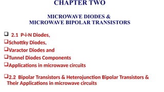
CHAPTER TWO
MICROWAVE DIODES&
MICROWAVE BIPOLAR TRANSISTORS
2.1 P-i-N Diodes,
Schottky Diodes,
Varactor Diodes and
Tunnel Diodes Components
Applications in microwave circuits
2.2 Bipolar Transistors & Heterojunction Bipolar Transistors &
Their Applications in microwave circuits
3.
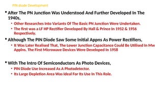
PIN diode Development
After The PN Junction Was Understood And Further Developed In The
1940s,
• Other Researches Into Variants Of The Basic PN Junction Were Undertaken.
• The first was a LF HP Rectifier Developed By Hall & Prince In 1952 & 1956
Respectively.
Although The PIN Diode Saw Some Initial Appns As Power Rectifiers,
• It Was Later Realised That, The Lower Junction Capacitance Could Be Utilised In Mw
Applns. The First Microwave Devices Were Developed In 1958
With The Intro Of Semiconductors As Photo Devices,
• PIN Diode Use Increased As A Photodetector.
• Its Large Depletion Area Was Ideal For Its Use In This Role.
4.
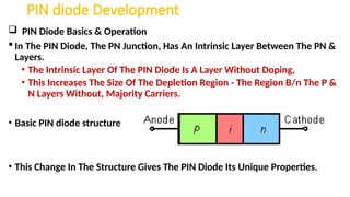
PIN diode Development
PIN Diode Basics & Operation
In The PIN Diode, The PN Junction, Has An Intrinsic Layer Between The PN &
Layers.
• The Intrinsic Layer Of The PIN Diode Is A Layer Without Doping,
• This Increases The Size Of The Depletion Region - The Region B/n The P &
N Layers Without, Majority Carriers.
• Basic PIN diode structure
• This Change In The Structure Gives The PIN Diode Its Unique Properties.
5.
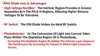
PIN Diode Uses& Advantages
• High Voltage Rectifier: The Intrinsic Region Provides A Greater
Separation B/n The PN & N Regions, Allowing Higher Reverse
Voltages To Be Tolerated.
• RF Switch: The PIN Diode Makes An Ideal RF Switch.
• Photodetector: As The Conversion Of Light Into Current Takes
Place Within The Depletion Region Of A Photodiode,
• Increasing The Depletion Region By Adding The Intrinsic Layer Improves
The Performance By Increasing He Volume In Which Light Conversion
Occurs.
6.
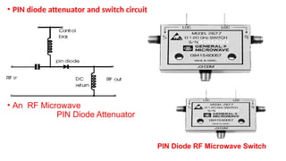
• PIN diodeattenuator and switch circuit
• An RF Microwave
PIN Diode Attenuator
PIN Diode RF Microwave Switch
7.
PIN DiodesAs Limiters:
• Used As Input Protection Devices For HF Test Probes.
• If The Input Signal Is Within Range, The PIN Diode Has Little
Impact As A Small Capacitance.
• If The Signal Is Large, Then The PIN Diode Conducts & Becomes A
Resistor That Shunts Most Of The Signal To Ground.
• Photodetector & Photovoltaic Cell
• PIN Photodiodes Are Used In Fibre Optic Network Cards &
Switches, As A Photodetector,
8.
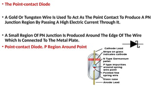
• The Point-contactDiode
• A Gold Or Tungsten Wire Is Used To Act As The Point Contact To Produce A PN
Junction Region By Passing A High Electric Current Through It.
• A Small Region Of PN Junction Is Produced Around The Edge Of The Wire
Which Is Connected To The Metal Plate.
• Point-contact Diode. P Region Around Point
9.
•In Forward DirectionIts Operation Is Quite Similar To The
PN Junction,
• But In Reverse Bias Condition, The Wire Acts Like An Insulator.
•The Insulator B/n The Junction Plates Acts As A Capacitor.
• In General The Capacitor Blocks The DC Currents When The AC
Currents Are Flowing In The Circuit At High Frequencies.
• So, These Are Used To Detect The High Frequency Signals.
10.
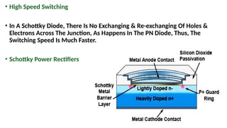
The Schottky Diode
•Schottky Diodes, Also Called Hot Carrier Diodes Or Schottky Barrier Diodes,
• Use A Metal/Semiconductor Junction Instead Of A P Semiconductor / N
Semiconductor Junction
Low Junction Potential
• The Metal To Silicon Junction Used In Schottky Diodes Provides Several
Advantages (& Some Disadvantages)
• Compared With A PN Silicon Diode.
• The P Type Region Of The PN Diode Is Replaced By A Metal Anode, Usually
Gold, Silver, Platinum, Tungsten, Molybdenum Or Chromium,
• Produce A Junction Potential Called The Schottky Barrier.
11.
Schottky Reverse CurrentLimitations
• Although The Schottky Junction Generates Less Heat Per Watt Than The PN
Junction,
• In Order To Keep Its Reverse Leakage Current Within Acceptable Limits,
• The Max Junction To
Must Be Kept Below Typically 125°C To 175°C
(Depending On Type)
• Compared With 200°C Or
More For A PN Diode.
12.
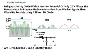
Schottky Diode Appns
•Using A Schottky Diode With A Junction Potential Of Only 0.2V Allows The
Demodulator To Produce Usable Information From Weaker Signals Than
Would Be Possible Using A Silicon PN Diode.
• Am Demodulation Using A Schottky Diode
13.
• High SpeedSwitching
• In A Schottky Diode, There Is No Exchanging & Re-exchanging Of Holes &
Electrons Across The Junction, As Happens In The PN Diode, Thus, The
Switching Speed Is Much Faster.
• Schottky Power Rectifiers
14.
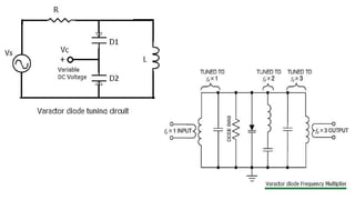
Varactor Diodes &Applications
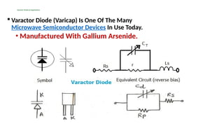
Varactor Diode (Varicap) Is One Of The Many
Microwave Semiconductor Devices In Use Today.
• Manufactured With Gallium Arsenide.
15.
• Varactor DiodeIs Special Type Of PN Junction Diode, In Which PN
Junction Capacitance Is Controlled Using Reverse Bias Voltage.
• When The Diode Is Forward Biased, Current Will Flow Through The
Diode.
• When The Diode Is Reverse Biased,
• Charges In The P And N Semiconductors Are Drawn Away From The PN
Junction Interface And Hence Forms The High Resistance Depletion Zone.
• The Equation Of The Varactor Capacitance Proportional To The
Reverse Bias Voltage Is: Cj = CK/(Vb - V)m
.
16.
• From TheCircuit Maximum Operating Frequency Of The Varactor
Diode Depends On The Series Resistance & Diode Capacitance & It
Is Mentioned In The Equation Below.
•F = 1 / 2*pi*Rs*Cj
• Quality Factor Of The Varactor Diode Is Mentioned In The Equation
Below.
Q = Fc/fo,
Where Fc Is The Cutoff Freq & fo Is The Operating Freq.
17.
Varactor Diode Applications
•FollowingAre The Varactor Diode Appns:
• It Is Used In Variable Resonant Tank LC Circuit.
• Afc(automatic Freq Control) Used To Set LO Signal.
• Frequency Modulator.
• Frequency Multiplier In Microwave Receiver LO.
• RF Phase Shifter.
19.
Tunnel Diodes
• ATunnel Diode Or Esaki Diode Is A Type Of Semiconductor That Is:
• Capable Of Very Fast Operation,
• Well Into The Mw Freq Region,
• Made Possible By The Use Of The Quantum Mechanical Effect Called Tunnelling.
• It Is A Two Terminal Device.
• The Concentration Of Dopants In Both P & N Region Is Very High.
• It Is About 1024
- 1025
m-3
• The P-n Junction Is Also Abrupt.
• For This Reasons,
• The Depletion Layer Width Is Very Small.
• In The Current Voltage Characteristics Of Tunnel Diode,
• We Can Find A Negative Slope Region When Forward Bias Is Applied.
20.
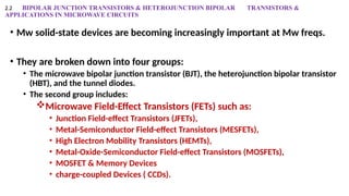
2.2 BIPOLAR JUNCTIONTRANSISTORS & HETEROJUNCTION BIPOLAR TRANSISTORS &
APPLICATIONS IN MICROWAVE CIRCUITS
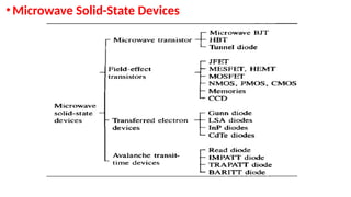
• Mw solid-state devices are becoming increasingly important at Mw freqs.
• They are broken down into four groups:
• The microwave bipolar junction transistor (BJT), the heterojunction bipolar transistor
(HBT), and the tunnel diodes.
• The second group includes:
Microwave Field-Effect Transistors (FETs) such as:
• Junction Field-effect Transistors (JFETs),
• Metal-Semiconductor Field-effect Transistors (MESFETs),
• High Electron Mobility Transistors (HEMTs),
• Metal-Oxide-Semiconductor Field-effect Transistors (MOSFETs),
• MOSFET & Memory Devices
• charge-coupled Devices ( CCDs).
21.
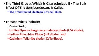
•The Third Group,Which Is Characterized By The Bulk
Effect Of The Semiconductor, Is Called:
• The Transferred Electron Device (TED).
•These devices include:
• Gunn diode,
• Limited Space-charge-accumulation diode (LSA diode),
• Indium Phosphide Diode (InP diode), and
• Cadmium Telluride diode ( CdTe diode).
22.
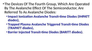
•The Devices OfThe Fourth Group, Which Are Operated
By The Avalanche Effect Of The Semiconductor, Are
Referred To As Avalanche Diodes:
•Impact Ionization Avalanche Transit-time Diodes (IMPATT
diodes),
•Trapped Plasma Avalanche Triggered Transit-time Diodes
(TRAPATT diodes),
•Barrier Injected Transit-time Diodes (BARITT diodes).
• In StudyingMicrowave Solid-state Devices, The Electrical Behavior Of
Solids Is The First Item To Be Investigated.
• The Transport Of Charge Thro A Semiconductor Depends Not Only On The
Properties Of The Electron;
• But Also On The Arrangement Of Atoms In The Solids.
• Semiconductors Are A Group Of Substances Having Electrical
Conductivities That Are Intermediate Between Metals & Insulators.
• Since The Conductivity Of The Semiconductors Can Be Varied Over Wide
Ranges By Changes In Their Temperature,
• Optical Excitation & Impurity Content,
• Thus, They Are The Natural Choices For Electronic Devices.
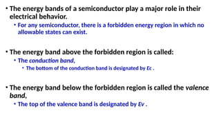
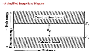
• The energybands of a semiconductor play a major role in their
electrical behavior.
• For any semiconductor, there is a forbidden energy region in which no
allowable states can exist.
• The energy band above the forbidden region is called:
• The conduction band,
• The bottom of the conduction band is designated by Ec .
• The energy band below the forbidden region is called the valence
band,
• The top of the valence band is designated by Ev .
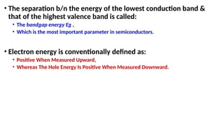
27.
• The separationb/n the energy of the lowest conduction band &
that of the highest valence band is called:
• The bandgap energy Eg ,
• Which is the most important parameter in semiconductors.
• Electron energy is conventionally defined as:
• Positive When Measured Upward,
• Whereas The Hole Energy Is Positive When Measured Downward.
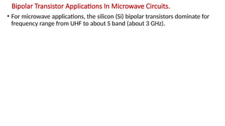
Bipolar Transistor ApplicationsIn Microwave Circuits.
• For microwave applications, the silicon (Si) bipolar transistors dominate for
frequency range from UHF to about S band (about 3 GHz).
30.
• The Sibipolar transistor is inexpensive, durable, integrative, and
offers gain much higher than available with competing field-effect
devices.
• It has moderate noise figure in RF amplifiers and 1/f noise
characteristics that are about 10-20 dB superior to GaAs MESFETs.
• For these reasons,
• The Si BJTs dominate in amplifier applications for the lower
microwave frequencies and are often the devices of choice for
local oscillators.
31.
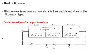
• Physical Structures
•All microwave transistors are now planar in form and almost all are of the
silicon n-p-n type.
• Carrier Densities of an n-p-n Transistor
• .
32.
• Bipolar TransistorConfigurations
• In General, There Are Two Types Of Bipolar Transistors: P-n-p And N-p-n.
• In Practical Applications, A Transistor Can Be Connected As Three Different
Configurations, Depending On The Polarities Of The Bias Voltages Connected
To Its Terminals:
• Common Base (CB),
• Common Emitter (CE), And
• Common Collector (CC),.
•
• Please to reflect on this, kindly refer to Electronics I Hand-out for the BTE
Programme
33.
• Principles ofOperation
• The Bipolar Junction Transistor (BJT) Is An Active Three-terminal Device
Which Is
• Commonly Used As An Amplifier Or Switch. Its Principles Of Operation Are
Discussed In This Section.
• Modes Of Operation. A Bipolar Transistor Can Operate In Four Different
• Modes Depending On The Voltage Polarities Across The Two Junctions:
• Normal (Active) Mode,
• Saturation Mode,
• Cutoff Mode, And
• Inverse (Or Inverted) Mode.
• Please Kindly Refer To Electronics I Hand-out For The Bte Programme
34.
• In ComparisonWith Si BJTs, Mw BJT Show Better
Performance In Terms Of:
• Emitter Injection Efficiency,
• Base Resistance,
• Base-emitter Capacitance, &
• Cutoff Frequency.
• They Also Offer Good Linearity, Low Phase Noise And High Power-added
Efficiency.
• Microwave BJT Applns
• Mw BJT Are Used In Both Commercial & High-reliability Appns, Such As PAs
In Mobile Telephones & Laser Drivers.
35.
HETEROJUNCTION BIPOLAR TRANSISTORS(HBTs}
• Bipolar Transistors Can Be Constructed As:
• Homojunction Or
• Heterojunction Types Of Transistors.
• When The Transistor Junction Is Jointed By Two Similar Materials Such As
Silicon To Silicon Or Germanium To Germanium,
• It Is A Homo Junction Transistor.
• The Transistor Junction Formed By Two Different Materials, Such As Ge To
Gaas, Is Called:
• A Heterojunction Transistor.
36.
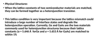
• Physical Structures
•When the lattice constants of two semiconductor materials are matched,
they can be formed together as a heterojunction transistor.
• This lattice condition is very important because the lattice mismatch could
introduce a large number of interface states and degrade the
heterojunction operation. Currently, Ge and GaAs are the two materials
commonly used for heterojunction structures because their lattice
constants (a = 5.646 Å forGe and a = 5.653 Å for GaAs) are matched to
within 1%
37.
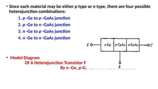
• Since eachmaterial may be either p type or n type, there are four possible
heterojunction combinations:
1. p -Ge to p -GaAs junction
2. p -Ge to n -GaAs junction
3. n -Ge to p -GaAs junction
4. n -Ge to n -GaAs junction
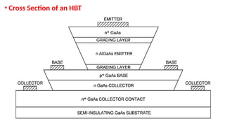
• Model Diagram
Of A Heterojunction Transistor Formed
By n -Ge, p-GaAs, and n-GaAs materials.
38.
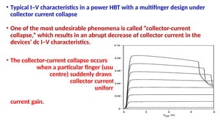
• Typical I–Vcharacteristics in a power HBT with a multifinger design under
collector current collapse
• One of the most undesirable phenomena is called “collector-current
collapse,” which results in an abrupt decrease of collector current in the
devices’ dc I–V characteristics.
• The collector-current collapse occurs
when a particular finger (usually
centre) suddenly draws most of the
collector current because of its non-
uniform current distribution, leading
to a decrease of device
current gain.
39.
• Although collector-currentcollapse has not been observed to
cause catastrophic failures on power HBTs,
• The output power and performance of the device are generally
limited.
• Optimized HBT layout improves power performance and
minimizes collector current collapse.
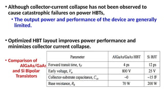
• Comparison of
AlGaAs/GaAs HBT
and Si Bipolar
Transistors
40.
• It followsthat AlGaAs/GaAs HBTs benefit from the following advantages:
•
• (1) Lower forward transit time along with a much lower base resistance (due to the
much higher base doping concentration), giving increased cutoff frequency Fc.
•
• 2) Better intrinsic device linearity due to a higher beta (gain) early-voltage product.
• (3) Very low collector-substrate capacitance Ccs in AlGaAs/GaAs HBTs due to the use of
semi-insulating GaAs substrate (resistivity ≈107 Ohm-cm).
• (4) High efficiency due to the ability to turn off devices completely with a small base
voltage change and the extremely small turn-on voltage variation between devices.
• (5) Good wide-band impedance matching due to the resistive nature of the input and
output impedances.
• (6) Low cost and potential for high throughput. With the typical minimum feature size
of 1 µm, there is no need for e-beam lithography.
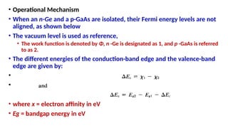
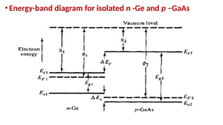
• Operational Mechanism
•When an n-Ge and a p-GaAs are isolated, their Fermi energy levels are not
aligned, as shown below
• The vacuum level is used as reference,
• The work function is denoted by Φ, n -Ge is designated as 1, and p -GaAs is referred
to as 2.
• The different energies of the conduction-band edge and the valence-band
edge are given by:
•
•
• where x = electron affinity in eV
• Eg = bandgap energy in eV
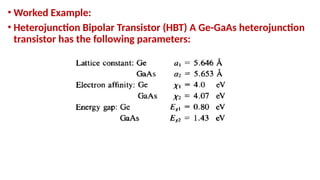
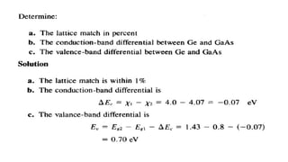
• Worked Example:
•Heterojunction Bipolar Transistor (HBT) A Ge-GaAs heterojunction
transistor has the following parameters:
46.
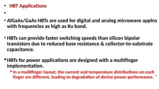
• HBT Applications
•
•AlGaAs/GaAs HBTs are used for digital and analog microwave applns
with frequencies as high as Ku band.
• HBTs can provide faster switching speeds than silicon bipolar
transistors due to reduced base resistance & collector-to-substrate
capacitance.
HBTs for power applications are designed with a multifinger
implementation.
In a multifinger layout, the current and temperature distributions on each
finger are different, leading to degradation of device power performance. ``
47.
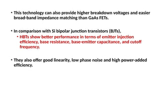
• This technologycan also provide higher breakdown voltages and easier
broad-band impedance matching than GaAs FETs.
• In comparison with Si bipolar junction transistors (BJTs),
• HBTs show better performance in terms of emitter injection
efficiency, base resistance, base-emitter capacitance, and cutoff
frequency.
• They also offer good linearity, low phase noise and high power-added
efficiency.
48.
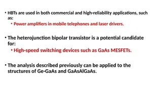
• HBTs areused in both commercial and high-reliability applications, such
as:
• Power amplifiers in mobile telephones and laser drivers.
• The heterojunction bipolar transistor is a potential candidate
for:
• High-speed switching devices such as GaAs MESFETs.
• The analysis described previously can be applied to the
structures of Ge-GaAs and GaAsAlGaAs.
49.
• The HBTis a potential candidate for high-speed switching devices,
• Such as GaAs MESFETs.
• The analysis described previously can be applied to the structures
of Ge-GaAs and GaAsAlGaAs.
• In other heterojunction transistors, such as the Ge-Si structure,
• The lattice mismatch (a = 5.646 Å forGe and a = 5.431 Å for Si) causes a
high interface state density & recombination- and tunneling-current
components must be counted.