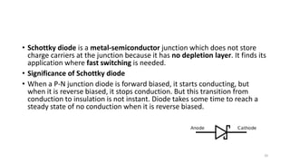
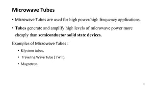
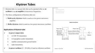
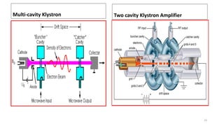
This document provides an overview of high power microwave devices and applications. It discusses the properties of microwaves and various microwave semiconductor devices like the Gunn diode, IMPATT diode, tunnel diode, and backward diode. It also covers microwave tubes such as the klystron, traveling wave tube (TWT), and magnetron. The document describes the operating principles and applications of these microwave devices in areas like wireless communications, radar, remote sensing, and industrial heating. It concludes with a brief discussion of waveguides and their use in transmitting microwave signals.
The document discusses various solid state microwave devices including varactor diodes, PIN diodes, Gunn diodes, and IMPATT diodes. It provides details on their operating principles and applications. Varactor diodes exploit the voltage-variable capacitance of a reverse biased PN junction and are used in voltage controlled oscillators and filters. PIN diodes act as switches and attenuators in microwave systems. Gunn diodes rely on negative differential resistance and are commonly used to generate microwave signals from 1-100 GHz. IMPATT diodes use avalanche breakdown and transit time delay to achieve negative resistance for oscillation at microwave frequencies.
A Gunn diode is a form of diode that exhibits negative resistance. It consists of a single piece of N-type semiconductor like gallium arsenide. When a voltage is applied, electrons are transferred into a third empty band, increasing their effective mass and decreasing their velocity. This creates a region of negative incremental resistance, where an increase in voltage causes resistance to increase. Gunn diodes are used as oscillators in radar, communications, and as sensors for intruder detection and measuring vibrations or rotational speed.
Optical detectors convert optical signals to electrical signals. Semiconductor-based photodiodes and phototransistors are commonly used, with photodiodes being used almost exclusively in fiber optic systems. The two main types of photodiodes are PIN photodiodes and avalanche photodiodes (APDs). PIN photodiodes consist of a wide, intrinsic semiconductor region sandwiched between p-type and n-type semiconductor regions. In a PIN photodiode, incident light generates electron-hole pairs which are separated by the electric field, resulting in a photocurrent. APDs use the avalanche effect to multiply the photocurrent, providing higher gain but greater noise.
Tunnel diodes have the following key properties:
1. They were invented in 1957 and work by allowing electrons to tunnel through a very narrow p-n junction using the quantum tunneling effect.
2. They have an unusual current-voltage characteristic with a negative-resistance region, which makes them useful for high-frequency oscillators.
3. Their main applications are in high-speed switching, signal detection, and frequency generation due to their ability to operate at frequencies into the microwave range resulting from their fast switching speeds.
special types of diodes Tunnel diode(1)03470719974
Tunnel diodes have the following key properties:
1. They were invented in 1957 and work by allowing electrons to tunnel through a very narrow p-n junction using the quantum tunneling effect.
2. They have an unusual current-voltage characteristic with a negative resistance region, which makes them useful for very high-frequency oscillators.
3. Their main applications are in high-speed computing, where they can switch on and off much faster than ordinary diodes due to the tunneling effect enabling faster electron movement.
This document discusses several types of special diodes:
- Tunnel diodes exploit the tunneling effect to conduct at very low voltages and exhibit negative resistance. They are used in oscillators.
- Schottky diodes have a metal-semiconductor junction and fast switching times, used in high-frequency applications.
- PIN diodes act as variable resistors when forward biased and capacitors when reverse biased, used in RF switching and modulation.
- Varactor diodes have variable capacitance when reverse biased, used in electronic tuning circuits.
The document discusses array detectors used in spectroscopy. It describes photodiode array detectors and charged coupled device (CCD) detectors. Photodiode array detectors contain an array of silicon photodiodes on a single chip that can simultaneously measure radiation intensities at all wavelengths. CCD detectors contain an array of linked capacitors that can transfer electric charges between neighboring capacitors, allowing detection of low intensity light signals. Both detector types offer advantages like low noise, wide spectral response, and simultaneous detection of emissions at different wavelengths.
The document discusses PIN diodes and varactor diodes. A PIN diode has a wide intrinsic semiconductor region between a p-type and n-type region, making it suitable for applications like attenuators and switches. It operates as a variable resistor at radio frequencies. A varactor diode provides a voltage-dependent variable capacitance and is used for electronic tuning and frequency multiplication. Both diodes have applications in radio frequency circuits due to their ability to dynamically control signal properties.
This document provides information about circular waveguides. It begins by defining a circular waveguide as a tubular circular conductor that supports TE or TM wave propagation modes. Cutoff wavelengths depend on the internal radius of the waveguide. Common modes for circular waveguides are labeled similarly to rectangular waveguides. The document also provides examples of calculating cutoff wavelengths and wavelengths in a guide for a given signal frequency and waveguide dimensions. It concludes by discussing microstrip and stripline transmission lines used at higher microwave frequencies when waveguides become impractical.
Diode data sheet for alarm type projectmegha agrawal
A diode is a two-terminal electronic component that allows current to pass in only one direction. It has low resistance to current in the forward direction and high resistance in the reverse direction. The most common use of diodes is for rectification, converting alternating current to direct current. When selecting a diode, its current handling capability, maximum reverse voltage, and forward voltage drop must be considered. Common types of diodes include silicon junction diodes, which have a p-n junction structure and exhibit asymmetric conduction. Diodes have applications in radio demodulation, power conversion, overvoltage protection, logic gates, and temperature measurement.
This document is a project report submitted to fulfill the requirements for a Bachelor of Science degree in Physics. It provides a PowerPoint presentation on solid state devices. The presentation introduces solid state devices and covers topics such as P and N type materials, PN junctions, diodes and their types including Zener diodes, transistors and their types, integrated circuits, and the advantages of solid state devices. It describes how silicon and germanium are used to make diodes and how dopants create P and N type materials. It also explains how PN junctions work and the differences between forward and reverse bias. Different types of diodes like LEDs and photodiodes are outlined along with their uses. The presentation concludes by
1) The document discusses different types of PN junction devices including PN junction diodes, rectifiers, LEDs, laser diodes, and Zener diodes.
2) It explains the structure and operation of PN junction diodes, describing how a PN junction is formed and how diffusion causes a depletion region and barrier potential.
3) The characteristics of PN junction diodes under forward and reverse bias are discussed, including their V-I characteristics and the factors that determine diode current.
Frequency-independent (FI) antennas are radiating structures capable of maintaining consistent impedance and pattern characteristics over multiple-decade bandwidths. Their finite size limits the lowest frequency of operation, and the finite precision of the center region bounds the highest frequency of operation.
1. The document discusses various methods for measuring linear and angular velocity, including electromagnetic, seismic, and digital transducers as well as using the Doppler effect.
2. Electromagnetic transducers are the most commonly used for linear velocity and work by inducing a voltage in a coil from the motion of a magnet. Moving magnet and moving coil types are described.
3. Angular velocity can be measured with a tachometer, which can be mechanical and count revolutions or electrical and generate a voltage proportional to speed.
This document contains a syllabus for a course on electronic devices. It outlines the topics to be covered, including semiconductor diodes, PN junction diodes, forward and reverse bias characteristics, bipolar junction transistors, tunnel diodes, SCRs, and unijunction transistors. The syllabus provides brief descriptions of key concepts such as intrinsic and extrinsic conduction in semiconductors, the depletion region and potential barrier in PN junctions, and the operation of common-emitter NPN transistors and tunnel diodes. Applications of devices like SCRs for power control and UJTs as trigger devices are also mentioned.
Types of Transducers
Analog and Digital Transducer
Characteristic of Transducer
Selection factor of Transducer
Measurement of Displacement
LVDT and RVDT
Different types of strain Gauges
Manometers
Pressure Measuring Elements
Hall Effect
Thermocouple
This document discusses the characteristics and applications of diodes. It begins by defining what a diode is - an electrical component that allows current to flow in only one direction. It then discusses the different types of diodes including PN junction diodes, Zener diodes, and light emitting diodes. The key characteristics and applications of each diode type are described. The document also covers the forward and reverse biasing of PN junction diodes and examines their V-I characteristics. Common questions about diodes are provided along with answers. Finally, the characteristics and applications of Zener diodes are discussed in more detail.
This document provides information about RF and microwave engineering:
1. It defines radio frequency as any electromagnetic wave frequency between 3KHz to 300GHz, which includes frequencies used for communications and radar signals. Microwaves are defined as electromagnetic waves between 300MHz to 300GHz.
2. Microwave engineering deals with the design of communication, navigation, and other systems that operate in the microwave frequency range. Key applications discussed include microwave ovens, radar, satellite communication, and TV.
3. Analysis of microwave circuits differs from low frequency circuits as the physical length of components is larger than signal wavelengths. S-parameters are used to relate the amplitude of scattered waves to incident waves in microwave circuit analysis.
A proximity sensor is a sensor able to detect the presence of nearby objects without any physical contact. It detects An Object When The Object Approaches Within The Detection Range And Boundary Of The Sensor. Proximity Sensor Includes All The Sensor That Perform Non-Contact Detection In Comparison To Sensors Such As Limit Switch, That Detect The Object By Physically Contacting Them. It is a sensor able to detect the presence of nearby objects without any physical contact
This document defines key terms and concepts related to photodetection for optical fiber communications. It discusses how photodetectors convert received optical signals to electrical signals and lists requirements for high performance. The main device types - PN photodiodes, are described. PN photodiodes work by generating electron-hole pairs when photons are absorbed in the depletion region, producing a photocurrent. Factors that determine a photodiode's response include absorption coefficient, quantum efficiency, and responsivity which is directly related to quantum efficiency. Materials properties also impact wavelength detection range.
PN JUNCTION DIODE CONSTRUCTION AND VI CHARACTERISTICSShobanaS19
The document provides a syllabus for the course EC 8351 Electronic Devices and Circuits. It outlines 5 units that will be covered: (1) PN junction devices including diodes and their characteristics; (2) transistors including BJT, JFET, MOSFET and their structure and characteristics; (3) amplifiers including small signal models and analysis of various amplifier configurations; (4) multistage amplifiers and differential amplifiers; and (5) feedback amplifiers and oscillators including various oscillator configurations. The syllabus provides a overview of the key topics and concepts that will be examined in the course.
This document discusses electromagnetic waves and their applications in circulators and isolators. It begins by explaining that circulators and isolators are nonreciprocal microwave devices that use Faraday rotation in ferrite materials. It then defines isolators as devices that isolate components from other reflections, allowing transmission in one direction while absorbing power in the opposite direction. Circulators are defined as multiport devices that allow wave transmission between ports in only one direction. The document proceeds to discuss the design and operating principles of isolators and circulators, including how ferrite materials introduce nonreciprocity. It explains how isolators and circulators are used to improve generator stability by preventing reflected power from returning. In summary, the document outlines the basic functions and
This document discusses electromagnetic waves and their applications in circulators and isolators. It begins by explaining that circulators and isolators are nonreciprocal microwave devices that use Faraday rotation in ferrite materials. It then defines isolators as devices that isolate components from other reflections, allowing transmission in one direction while absorbing power in the opposite direction. Circulators are defined as multiport devices that allow wave transmission between ports in only one direction. The document proceeds to discuss the design and operating principles of isolators and three-port and four-port circulators. It concludes by noting various types of circulators are used based on the same nonreciprocal principles.
Microwave devices can be passive or active. Passive devices include terminations to absorb microwave power without reflection, as well as directional couplers and phase shifters. Terminations include matched loads made of lossy materials placed in waveguides to absorb all incident power. Directional couplers are four-port devices that couple power between two connected waveguides in one direction only. Phase shifters provide a variable phase shift without changing the physical path length using materials like ferrites or dielectrics.
Network analysis of rf and microwave circuitsShankar Gangaju
This document discusses microwave network analysis and two-port network analysis. It begins by defining a microwave network as consisting of microwave devices and components coupled by transmission lines. It then discusses that at microwave frequencies, circuit analysis techniques like KCL and KVL cannot be used and S-parameters provide an alternative. The document defines S-parameters as a way to characterize networks using normalized power waves rather than voltages and currents. It provides properties and definitions of S-parameters for two-port networks, including what S11, S12, S21, and S22 represent. It also discusses uses of S-parameters and scattering matrices for modeling networks.
Non-destructive testing (NDT) involves analysis techniques used to evaluate materials, components, or systems without damaging them. NDT is used to determine properties like resistivity, dielectric constant, and loss factor of insulating materials. It helps ensure materials maintain their insulating properties during operation. Two common methods for measuring dielectric loss and loss angle of insulating materials are the Schering bridge and transformer ratio arm bridge. The loss angle tan δ indicates the quality of insulation and can determine material life expectancy. Partial discharges within insulating materials are detected using NDT and indicate weaknesses.
Google Calendar is a versatile tool that allows users to manage their schedules and events effectively. With Google Calendar, you can create and organize calendars, set reminders for important events, and share your calendars with others. It also provides features like creating events, inviting attendees, and accessing your calendar from mobile devices. Additionally, Google Calendar allows you to embed calendars in websites or platforms like SlideShare, making it easier for others to view and interact with your schedules.
1. High Power Microwave Devices &
Applications
By
Prof. Gloria Chukwudebe
Department of Electrical and Electronic Engineering
Federal University of Technology, Owerri
1
2. Outline
• Introduction
• Properties of Microwaves
• Applications Of Microwaves
• Advantages of Microwave Communication
• Microwave semiconductor devices: Backward, Gunn, Impatt,
Schottky, Tunnel diodes, etc.
• Microwave Tubes: Klystron , Traveling Wave Tube, Magnetron, etc
• Waveguides.
2
3. Introduction
• Microwaves have frequencies > 1 GHz approx.
• Stray reactances become important as frequency increases.
• Cable losses increase as frequency increases, waveguides often used instead.
• To generate such high-power microwaves:
• Semiconductor devices or
• Tubes are used.
• Semiconductor devices are mostly diodes made of Gallium Arsenide or
Indium Phosphide while Tubes are made of metallic cylinders that use CRT
technology
• The Microwave Tubes are designed to transform the energy of an intense electron
beam into electromagnetic radiation at microwave frequencies.
3
4. 4
Properties of Microwaves
1. Microwave is an electromagnetic radiation of short wavelength.
2. They can reflected by conducting surfaces just like optical waves
since they travel in straight line.
3. Microwave currents flow through a thin outer layer of an ordinary
cable.
4. Microwaves are easily attenuated within short distances.
5. They are not reflected by ionosphere
5. Applications Of Microwaves
• Wireless Communications (space, cellular phones, cordless phones, WLANs, Bluetooth, satellites etc.)
• Radar and Navigation (Airborne,vehicle, weather radars, GPS etc.)
• Remote sensing (Meteorology, mining, land surface, aviation and marine traffic etc.)
• RF Identification (Security, product tracking, animal tracking, toll collection etc.)
• Broadcasting (AM,FM radio, TV etc.)
• Heating (Baking, Food process, Ovens, Drying, Mining, rubber industry)
• Bio-medical application(Diagnostics)
Advantage of Microwave Communication
Power requirement is very less compared to LF signals
Larger Bandwidth : The band width of microwaves is larger than the low frequency signals - more
information can be transmitted using single carrier
Improved directive properties
Less Fading effect and more reliable
5
9. • Applications of Gunn Diode
• Gunn Diodes are used as oscillators and Amplifiers.
• They are used in radio communication, military and commercial radar sources.
• Gunn diodes are used as fast controlling equipment in microelectronics for modulation of
laser beams.
• It is used in tachometers.
• Gunn diode is used in sensors for detection in trespass detecting system, in-door opening
system, pedestrian safety systems etc.
• It is also used extensively in microwave relay data link transmitters.
• These are the advantages, disadvantages and applications of Gunn diode. These are
extensively used in sensors in the detection system.
9
10. • Gunn diodes are also known as transferred electron devices, TED, are widely used in microwave RF
applications for frequencies between 1 and 100 GHz. •
• The Gunn diode is most commonly used for generating microwave RF signals - these circuits may also
be called a transferred electron oscillator or TEO. The Gunn diode may also be used for an amplifier in
what may be known as a transferred electron amplifier or TEA.
• 4-100hz
• The Gunn diode operation depends on the fact that it has a voltage controlled negative resistance.
• Gunn diodes are fabricated from a single piece of n-type semiconductor. The most common materials
are gallium Arsenide, GaAs and Indium Phosphide, InP. However other materials including Ge, CdTe,
InAs, InSb, ZnSe and others have been used. The device is simply an n-type bar with n+ contacts. It is
necessary to use n-type material because the transferred electron effect is only applicable to electrons
and not holes found in a p-type material
10
13. • A backward diode is a semiconductor device which works in reversed biased mode. It is designed by
providing variation in the design characteristics of Zener diode and tunnel diode. It is unilateral device
because its designing mechanism allows it to operate in one direction only.
• Structure of Backward Diode
• The construction of backward diode is similar to that of the tunnel diode. One side of the junction is lightly
doped and another side of the junction is heavily doped. The characteristics so generated resembles the
characteristics of the tunnel diode.
• The operation of the diode takes place in reverse biasing mode thus, it is called backward diode.
• Applications- oscilators, mixer,
• Application of Backward Diode
• Detector: It can be used as a detector up to the frequency of 40 GHz. It possesses low capacitance thus the
problem of charge storage is minimized in these diodes. Besides, it’s nonlinear characteristics for small signal
makes it appropriate for application of detector.
• Switch: The low capacitance of these diodes imparts an ability to the diode to switch from On state to off
state efficiently. Thus, it is used in switching circuitry.
13
14. • The device exhibits a negative resistance region on its V/I curve as
seen below. This negative resistance area enables the Gunn diode to
amplify signals. This can be used both in amplifiers and oscillators.
However Gunn diode oscillators are the most commonly found
• This negative resistance region means that the current flow in diode
increases in the negative resistance region when the voltage falls - the
inverse of the normal effect in any other positive resistance element.
14
15. • Sensors and measuring instruments ▫ Gunn diode oscillators are used
to generate microwave power for: airborne collision avoidance radar,
antilock brakes, sensors for monitoring the flow of traffic, car radar
detectors, pedestrian safety systems, "distance traveled" recorders,
motion detectors, "slowspeed" sensors (to detect pedestrian and
traffic movement up to 50 m.p.h), traffic signal controllers, automatic
door openers, automatic traffic gates, process control equipment to
monitor throughput, burglar alarms and equipment to detect
trespassers, sensors to avoid derailment of trains, remote vibration
detectors, rotational speed tachometers, moisture content monitors
15
16. • IMPATT Diode • Impact Avalanche and Transit-Time (IMPATT) Diode, also
called Avalanche transit-time diodes • Multilayer diodes of several
different types used to generate microwave power
• In contrast to other devices in this class (tunnel diodes, thyristors, and
Gunn diodes), the negative resistance of avalanche-and-transit time diodes
appears only at superhigh frequencies. • Avalanche-and-transit time diodes
are used to generate oscillations in the frequency range from 1 to 300
gigahertz • Avalanche-and-transit time diodes can be made from structures
of the p +-n-i-n + type (the Read diode) or the p-i-n, p-n, p+-n, and p-n +
types
16
17. • IMPATT Diode - Operation • As a result they collide with the crystal lattice and free other carriers. These newly freed carriers are
similarly accelerated and collide with the crystal lattice freeing more carriers. This process gives rise to what is termed avalanche
breakdown as the number of carriers multiplies very quickly. For this type of breakdown only occurs when a certain voltage is
applied to the junction. Below this the potential does not accelerate the carriers sufficiently.
• Once the carriers have been generated the device relies on negative resistance to generate and sustain an oscillation. The effect
does not occur in the device at DC, but instead, here it is an AC effect that is brought about by phase differences that are seen at
the frequency of operation. When an AC signal is applied the current peaks are found to be 180 degrees out of phase with the
voltage. This results from two delays which occur in the device: injection delay, and a transit time delay as the current carriers
migrate or drift across the device.
• The voltage applied to the IMPATT diode has a mean value that means the diode is on the verge of avalanche breakdown. The
voltage varies as a sine wave, but the generation of carriers does not occur in unison with the voltage variations. It might be
expected that it would occur at the peak voltage. This arises because the generation of carriers is not only a function of the electric
field but also the number of carriers already in existence.
• As the electric field increases so does the number of carriers. Then even after the field has reached its peak the number of carriers
still continues to grow as a result of the number of carriers already in existence. This continues until the field falls to below a
critical value when the number of carriers starts to fall. As a result of this effect there is a phase lag so that the current is about 90
degrees behind the voltage. This is known as the injection phase delay. • When the electrons move across the N+ region an
external current is seen, and this occurs in peaks, resulting in a repetitive waveform.
17
19. • Tunnel Diode
• Definition: Tunnel diode is a heavily doped diode which possesses high conductivity due to the higher
concentration of impurity atoms. It is different from a conventional P-N junction in terms of doping density.
• Applications of Tunnel Diode
• It is used as a switch, oscillator, amplifier etc. It can be used as a high-frequency component because of its
fast response, but due to the availability of better devices, it is not preferred.
19
20. • Schottky diode is a metal-semiconductor junction which does not store
charge carriers at the junction because it has no depletion layer. It finds its
application where fast switching is needed.
• Significance of Schottky diode
• When a P-N junction diode is forward biased, it starts conducting, but
when it is reverse biased, it stops conduction. But this transition from
conduction to insulation is not instant. Diode takes some time to reach a
steady state of no conduction when it is reverse biased.
20
21. • Microwave Tubes are used for high power/high frequency applications.
• Tubes generate and amplify high levels of microwave power more
cheaply than semiconductor solid state devices.
Examples of Microwave Tubes :
• Klystron tubes,
• Traveling Wave Tube (TWT),
• Magnetron.
Microwave Tubes
21
22. • Klystron tube is a vacuum tube that can be operated either as an
oscillator or as an amplifier at microwave frequencies.
• Two basic configurations of klystron tubes are :
1. Multi-cavity klystron which is used as a low power microwave
amplifier.
2. Reflex klystron which is used as a low power microwave oscillator.
Applications of Klystron tube
As power output tubes
1. in UHF TV transmitters
2. in troposphere scatter transmitters
3. satellite communication ground station
4. radar transmitters
As power oscillator (5 – 50 GHz), if used as a klystron oscillator
Klystron Tubes
22
Klystron Tube Operation
• Electron beam moves down tube past several cavities.
• Input cavity is the buncher, output cavity is the catcher.
• Buncher modulates the velocity of the electron beam
24. Mechanism of operation of Reflex Klystron
24
A reflex klystron consists of an electron gun, an
accelerating grid, a single re-entrant cavity and a
repeller plate.
Electrons emitted from cathode is accelerated by the
grid and passes through the cavity-anode to the
repeller space.
Due to DC energy, RF noise is generated in the cavity.
Electrons passing through cavity gap experiences
Velocity Modulation.
• the velocity modulated electrons are bunched together
and lose their kinetic energy when they encounter the
positive peak of the cavity RF field.
This loss of energy is transferred to the cavity to
conserve total power.
When power delivered by the electrons is equal to the
power loss in the cavity- Microwave oscillation is
started.
25. The reflex klystrons are used in
1. Radar receivers
2. Local oscillator in microwave receivers
3. Signal source in microwave generator of variable frequency
4. Portable microwave links
5. Pump oscillator in parametric amplifier
Applications of Reflex Klystrons
25
26. • TWT is an amplifier that makes use of distributed interaction between electron
beam and a travelling wave.
• It is mainly used for amplification of high frequencies. i.e. 3000 MHz or above.
• Its principle feature is based on a slow wave structure.
• The RF wave propagate at the speed of light, while electron beam propagate at
much slow velocity.
• Therefore the mechanism that reduces RF wave phase velocity in a TWT is a
slow wave structure.
Traveling Wave Tube (TWT)
26
27. Traveling-Wave Tube (TWT) features
The unique feature of the TWT is a helix or coil
that surrounds the length of the tube and the
electron beam passes through the centre or
axis of the helix.
The microwave signal to be amplified is applied
to the end of the helix near the cathode and
the output is taken from the end of the helix
near the collector (anode).
The purpose of the helix is to provide path for
RF signal (slow-wave structure)
Energy is transferred from electron beam to
microwaves.
The propagation of the RF signal along the helix
is made approximately equal to the velocity of
the electron beam from the cathode to the
anode.
Structure of Traveling-Wave Tube (TWT)
27
28. 28
Traveling-Wave Tube Operation
The passage of the microwave signal down the helix produces electric and magnetic
fields that will interact with the electron beam.
The electromagnetic field produced by the helix causes the electrons to be speeded up
and slowed down, this produces velocity modulation of the beam which produces
density modulation.
Density modulation causes bunches of electrons to group together one wavelength
apart and these bunch of electrons travel down the length of the tube toward the
collector.
The electron bunches induce voltages into the helix which reinforce the voltage already
present there. Due to that, the strength of the electromagnetic field on the helix
increases as the wave travels down the tube towards the collector.
At the end of the helix, the signal is considerably amplified.
Coaxial cable or waveguide structures are used to extract the energy from the helix.
29. Applications of TWT
1. Low noise RF amplifier in broad band microwave
receivers.
2. Repeater amplifier in wide band communication
links and long distance telephony.
3. Due to long tube life (50,000 hours against ¼th for
other types), TWT is used as power output tube
in communication satellites.
4. Continuous wave high power TWT’s are used in
troposcatter links (due to larger power and larger
bandwidths).
5. Used in Air borne and ship borne pulsed high
power radars.
Benefits of TWT
1. TWT has extremely wide bandwidth.
Hence, it can be made to amplify signals
from UHF to hundreds of gigahertz.
2. Most of the TWTs have a frequency range
of approximately 2:1 in the desired
segment of the microwave region to be
amplified.
3. The TWTs can be used in both continuous
and pulsed modes of operation with power
levels up to several thousands watts.
29
30. • Magnetron is a high-power microwave
oscillator.
• Common in radar and microwave ovens.
• Cathode in center, anode around outside.
• Strong DC magnetic field around tube causes
electrons from cathode to spiral as they move
toward anode.
• Current of electrons generates microwaves in
cavities around outside.
Magnetron
30
31. • Magnetron has a Slow-Wave Structure,
there are cavities all around the outside.
• Wave circulates from one cavity to the next
around the outside.
• Each cavity represents one-half period.
• Wave moves around tube at a velocity
much less than that of light.
• Wave velocity approximately equals
electron velocity.
Magnetron ctd
31
33. Waveguides
• Pipe through which waves propagate
• Can have various cross sections
• Rectangular
• Circular
• Elliptical
• Can be rigid or flexible
• Waveguides have very low loss
Modes
• Waves can propagate in various ways
• Time taken to move down the guide varies with the mode
• Each mode has a cutoff frequency below which it won’t propagate
• Mode with lowest cutoff frequency is dominant mode
33