1. The document provides instructions on how to generate a layout view in Cadence Virtuoso and perform layout verification and simulation with extracted parasitics. It describes creating a CMOS inverter layout including placing nFET and pFET devices and connecting their terminals.
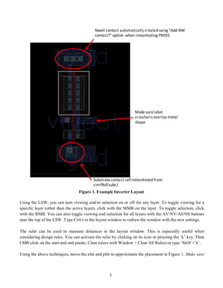
2. Key layers used in the layout are described, including Metal 1 (M1), Poly (PC), Diffusion (RX), Contact (CA), N-well (NW), P+ implant (BP), and Via 1 (V1). Design rules for spacing and dimensions are outlined.
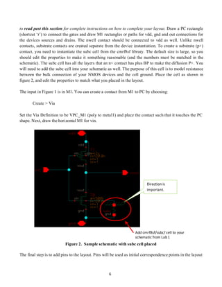
3. An example inverter layout is shown, and instructions are provided on how to move and edit devices, enter layout shapes, and connect the devices to