This document provides information on the IRFZ24NPbF HEXFET power MOSFET from International Rectifier. It has a low on-resistance of 0.07 ohms and is suitable for applications up to 50 watts. The MOSFET uses a TO-220 package for its low thermal resistance and cost. It has features such as fast switching, avalanche rating, and a wide operating temperature range from -55 to 175 degrees Celsius.
Original N-Channel Power MOSFET IRF1010EPBF IRF1010 1010 60V 84A TO-220 New I...AUTHELECTRONIC
Original N-Channel Power MOSFET IRF1010EPBF IRF1010 1010 60V 84A TO-220 New International Rectifier
https://authelectronic.com/original-n-channel-power-mosfet-irf1010epbf-irf1010-1010-60v-84a-to-220-new-international-rectifier
Original N Channel Mosfet IRF630N IRF630 TO-220 9.3A 200V New IRAUTHELECTRONIC
Original N Channel Mosfet IRF630N IRF630 TO-220 9.3A 200V New IR
https://authelectronic.com/original-n-channel-mosfet-irf630n-irf630-to-220-9-3a-200v-new-ir
Original P-CHANNEL MOSFET IRF5210PBF IRF5210 5210 100V 38A TO-220 New IRAUTHELECTRONIC
Original P-CHANNEL MOSFET IRF5210PBF IRF5210 5210 100V 38A TO-220 New IR
https://authelectronic.com/original-p-channel-mosfet-irf5210pbf-irf5210-5210-100v-38a-to-220-new-ir
Original N-channel 650 V 0.230 Ohm 12 A MDmesh V Power MOSFET in DPAK DPAK ST...AUTHELECTRONIC
Original N-channel 650 V 0.230 Ohm 12 A MDmesh V Power MOSFET in DPAK DPAK STF16N65M5 16N65M5 16N65 710V 12A TO-220FP New STMicroelectronics
https://authelectronic.com/original-n-channel-650-v-0-230-ohm-12-a-mdmesh-v-power-mosfet-in-dpak-dpak-stf16n65m5-16n65m5-16n65-710v-12a-to-220fp-new-stmicroelectronics
Original Mosfet IRFB18N50KPBF IRFB18N50K FB18N50K 18N50K 500V 17A TO-220 New ...AUTHELECTRONIC
Original Mosfet IRFB18N50KPBF IRFB18N50K FB18N50K 18N50K 500V 17A TO-220 New International Rectifier
https://authelectronic.com/original-mosfet-irfb18n50kpbf-irfb18n50k-fb18n50k-18n50k-500v-17a-to-220-new-international-rectifier
Original Power MOSFET IRFP460PBF IRFP460 460 500V 20A TO-247 New Vishay Silic...AUTHELECTRONIC
Original Power MOSFET IRFP460PBF IRFP460 460 500V 20A TO-247 New Vishay Siliconix
https://authelectronic.com/original-power-mosfet-irfp460pbf-irfp460-460-500v-20a-to-247-new-vishay-siliconix
Original N-CHANNEL Mossfet IRFB4227PBF IRFB4227 4227 130A 200V TO-220 New IRAUTHELECTRONIC
Original N-CHANNEL Mossfet IRFB4227PBF IRFB4227 4227 130A 200V TO-220 New IR
https://authelectronic.com/original-n-channel-mossfet-irfb4227pbf-irfb4227-4227-130a-200v-to-220-new-ir
Original N Channel Mosfet IRF3710PBF IRF3710 3710 37A 100V NewAUTHELECTRONIC
Original N Channel Mosfet IRF3710PBF IRF3710 3710 37A 100V New
https://authelectronic.com/original-n-channel-mosfet-irf3710pbf-irf3710-3710-37a-100v-new
Original Power MOSFET IRFP140PBF IRFP140 IRFP140N 100V 33A TO-247 New Intern...AUTHELECTRONIC
Original Power MOSFET IRFP140PBF IRFP140 IRFP140N 100V 33A TO-247 New International Rectifier
https://authelectronic.com/original-power-mosfet-irfp140pbf-irfp140-irfp140n-100v-33a-to-247-new-international-rectifier
Original N-Channel Mosfet IRFI4019H-117P 4019 8A 150V TO-220 NewAUTHELECTRONIC
Original N-Channel Mosfet IRFI4019H-117P 4019 8A 150V TO-220 New
https://authelectronic.com/original-n-channel-mosfet-irfi4019h-117p-4019-8a-150v-to-220-new
Original N-Channel Mosfet IRFI4019H-117P 4019 8A 150V TO-220 NewAUTHELECTRONIC
Original N-Channel Mosfet IRFI4019H-117P 4019 8A 150V TO-220 New
https://authelectronic.com/original-n-channel-mosfet-irfi4019h-117p-4019-8a-150v-to-220-new
Original P Channel Mosfet IRF9Z34 IRF9Z34N IRF9Z34NPBF 9Z34 60V 18A TO 220 NewAUTHELECTRONIC
Original P Channel Mosfet IRF9Z34 IRF9Z34N IRF9Z34NPBF 9Z34 60V 18A TO 220 New
https://authelectronic.com/original-p-channel-mosfet-irf9z34-irf9z34n-irf9z34npbf-9z34-60v-18a-to-220-new
Original N Channel Mosfet FQPF12N60 12N60 12A 600V New FairchildAUTHELECTRONIC
Original N Channel Mosfet FQPF12N60 12N60 12A 600V New Fairchild
https://authelectronic.com/original-n-channel-mosfet-fqpf12n60-12n60-12a-600v-new-fairchild
Original Dual P-Channel Mosfet RF7316TRPBF IRF7316 F7316 7316 SOP-8 New IRAUTHELECTRONIC
Original Dual P-Channel Mosfet RF7316TRPBF IRF7316 F7316 7316 SOP-8 New IR
https://authelectronic.com/original-dual-p-channel-mosfet-rf7316trpbf-irf7316-f7316-7316-sop-8-new-ir
Original N-Channel Mosfet IRF2907ZPBF 2907 75V 170A TO-220 New IRAUTHELECTRONIC
Original N-Channel Mosfet IRF2907ZPBF 2907 75V 170A TO-220 New IR
https://authelectronic.com/original-n-channel-mosfet-irf2907zpbf-2907-75v-170a-to-220-new-ir
Welcome to WIPAC Monthly the magazine brought to you by the LinkedIn Group Water Industry Process Automation & Control.
In this month's edition, along with this month's industry news to celebrate the 13 years since the group was created we have articles including
A case study of the used of Advanced Process Control at the Wastewater Treatment works at Lleida in Spain
A look back on an article on smart wastewater networks in order to see how the industry has measured up in the interim around the adoption of Digital Transformation in the Water Industry.
Sachpazis:Terzaghi Bearing Capacity Estimation in simple terms with Calculati...Dr.Costas Sachpazis
Terzaghi's soil bearing capacity theory, developed by Karl Terzaghi, is a fundamental principle in geotechnical engineering used to determine the bearing capacity of shallow foundations. This theory provides a method to calculate the ultimate bearing capacity of soil, which is the maximum load per unit area that the soil can support without undergoing shear failure. The Calculation HTML Code included.
Industrial Training at Shahjalal Fertilizer Company Limited (SFCL)MdTanvirMahtab2
This presentation is about the working procedure of Shahjalal Fertilizer Company Limited (SFCL). A Govt. owned Company of Bangladesh Chemical Industries Corporation under Ministry of Industries.
Immunizing Image Classifiers Against Localized Adversary Attacksgerogepatton
This paper addresses the vulnerability of deep learning models, particularly convolutional neural networks
(CNN)s, to adversarial attacks and presents a proactive training technique designed to counter them. We
introduce a novel volumization algorithm, which transforms 2D images into 3D volumetric representations.
When combined with 3D convolution and deep curriculum learning optimization (CLO), itsignificantly improves
the immunity of models against localized universal attacks by up to 40%. We evaluate our proposed approach
using contemporary CNN architectures and the modified Canadian Institute for Advanced Research (CIFAR-10
and CIFAR-100) and ImageNet Large Scale Visual Recognition Challenge (ILSVRC12) datasets, showcasing
accuracy improvements over previous techniques. The results indicate that the combination of the volumetric
input and curriculum learning holds significant promise for mitigating adversarial attacks without necessitating
adversary training.
Final project report on grocery store management system..pdfKamal Acharya
In today’s fast-changing business environment, it’s extremely important to be able to respond to client needs in the most effective and timely manner. If your customers wish to see your business online and have instant access to your products or services.
Online Grocery Store is an e-commerce website, which retails various grocery products. This project allows viewing various products available enables registered users to purchase desired products instantly using Paytm, UPI payment processor (Instant Pay) and also can place order by using Cash on Delivery (Pay Later) option. This project provides an easy access to Administrators and Managers to view orders placed using Pay Later and Instant Pay options.
In order to develop an e-commerce website, a number of Technologies must be studied and understood. These include multi-tiered architecture, server and client-side scripting techniques, implementation technologies, programming language (such as PHP, HTML, CSS, JavaScript) and MySQL relational databases. This is a project with the objective to develop a basic website where a consumer is provided with a shopping cart website and also to know about the technologies used to develop such a website.
This document will discuss each of the underlying technologies to create and implement an e- commerce website.
NO1 Uk best vashikaran specialist in delhi vashikaran baba near me online vas...Amil Baba Dawood bangali
Contact with Dawood Bhai Just call on +92322-6382012 and we'll help you. We'll solve all your problems within 12 to 24 hours and with 101% guarantee and with astrology systematic. If you want to take any personal or professional advice then also you can call us on +92322-6382012 , ONLINE LOVE PROBLEM & Other all types of Daily Life Problem's.Then CALL or WHATSAPP us on +92322-6382012 and Get all these problems solutions here by Amil Baba DAWOOD BANGALI
#vashikaranspecialist #astrologer #palmistry #amliyaat #taweez #manpasandshadi #horoscope #spiritual #lovelife #lovespell #marriagespell#aamilbabainpakistan #amilbabainkarachi #powerfullblackmagicspell #kalajadumantarspecialist #realamilbaba #AmilbabainPakistan #astrologerincanada #astrologerindubai #lovespellsmaster #kalajaduspecialist #lovespellsthatwork #aamilbabainlahore#blackmagicformarriage #aamilbaba #kalajadu #kalailam #taweez #wazifaexpert #jadumantar #vashikaranspecialist #astrologer #palmistry #amliyaat #taweez #manpasandshadi #horoscope #spiritual #lovelife #lovespell #marriagespell#aamilbabainpakistan #amilbabainkarachi #powerfullblackmagicspell #kalajadumantarspecialist #realamilbaba #AmilbabainPakistan #astrologerincanada #astrologerindubai #lovespellsmaster #kalajaduspecialist #lovespellsthatwork #aamilbabainlahore #blackmagicforlove #blackmagicformarriage #aamilbaba #kalajadu #kalailam #taweez #wazifaexpert #jadumantar #vashikaranspecialist #astrologer #palmistry #amliyaat #taweez #manpasandshadi #horoscope #spiritual #lovelife #lovespell #marriagespell#aamilbabainpakistan #amilbabainkarachi #powerfullblackmagicspell #kalajadumantarspecialist #realamilbaba #AmilbabainPakistan #astrologerincanada #astrologerindubai #lovespellsmaster #kalajaduspecialist #lovespellsthatwork #aamilbabainlahore #Amilbabainuk #amilbabainspain #amilbabaindubai #Amilbabainnorway #amilbabainkrachi #amilbabainlahore #amilbabaingujranwalan #amilbabainislamabad
Hierarchical Digital Twin of a Naval Power SystemKerry Sado
A hierarchical digital twin of a Naval DC power system has been developed and experimentally verified. Similar to other state-of-the-art digital twins, this technology creates a digital replica of the physical system executed in real-time or faster, which can modify hardware controls. However, its advantage stems from distributing computational efforts by utilizing a hierarchical structure composed of lower-level digital twin blocks and a higher-level system digital twin. Each digital twin block is associated with a physical subsystem of the hardware and communicates with a singular system digital twin, which creates a system-level response. By extracting information from each level of the hierarchy, power system controls of the hardware were reconfigured autonomously. This hierarchical digital twin development offers several advantages over other digital twins, particularly in the field of naval power systems. The hierarchical structure allows for greater computational efficiency and scalability while the ability to autonomously reconfigure hardware controls offers increased flexibility and responsiveness. The hierarchical decomposition and models utilized were well aligned with the physical twin, as indicated by the maximum deviations between the developed digital twin hierarchy and the hardware.
Pile Foundation by Venkatesh Taduvai (Sub Geotechnical Engineering II)-conver...
Original N-Channel Mosfet IRFZ24N IRFZ24 TO-220 New Infineon Technologies
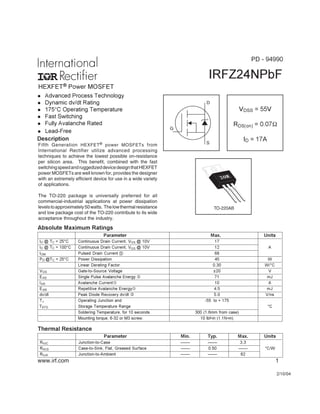
1. HEXFET® Power MOSFET
IRFZ24NPbF
Fifth Generation HEXFET® power MOSFETs from
International Rectifier utilize advanced processing
techniques to achieve the lowest possible on-resistance
per silicon area. This benefit, combined with the fast
switchingspeedandruggedizeddevicedesignthatHEXFET
power MOSFETs are well known for, provides the designer
with an extremely efficient device for use in a wide variety
of applications.
The TO-220 package is universally preferred for all
commercial-industrial applications at power dissipation
levelstoapproximately50watts. Thelowthermalresistance
and low package cost of the TO-220 contribute to its wide
acceptance throughout the industry.
l Advanced Process Technology
l Dynamic dv/dt Rating
l 175°C Operating Temperature
l Fast Switching
l Fully Avalanche Rated
Description
2/10/04
VDSS = 55V
RDS(on) = 0.07Ω
ID = 17AS
D
G
TO-220AB
Parameter Min. Typ. Max. Units
RθJC Junction-to-Case –––– –––– 3.3
RθCS Case-to-Sink, Flat, Greased Surface –––– 0.50 –––– °C/W
RθJA Junction-to-Ambient –––– –––– 62
Thermal Resistance
Parameter Max. Units
ID @ TC = 25°C Continuous Drain Current, VGS @ 10V 17
ID @ TC = 100°C Continuous Drain Current, VGS @ 10V 12 A
IDM Pulsed Drain Current # 68
PD @TC = 25°C Power Dissipation 45 W
Linear Derating Factor 0.30 W/°C
VGS Gate-to-Source Voltage ±20 V
EAS Single Pulse Avalanche Energy ‚ 71 mJ
IAR Avalanche Current 10 A
EAR Repetitive Avalanche Energy 4.5 mJ
dv/dt Peak Diode Recovery dv/dt ƒ 5.0 V/ns
TJ Operating Junction and -55 to + 175
TSTG Storage Temperature Range °C
Soldering Temperature, for 10 seconds 300 (1.6mm from case)
Mounting torque, 6-32 or M3 screw. 10 lbf•in (1.1N•m)
Absolute Maximum Ratings
www.irf.com 1
PD - 94990
l Lead-Free
2. IRFZ24NPbF
2 www.irf.com
Parameter Min. Typ. Max. Units Conditions
V(BR)DSS Drain-to-Source Breakdown Voltage 55 ––– ––– V VGS = 0V, ID = 250µA
∆V(BR)DSS/∆TJ Breakdown Voltage Temp. Coefficient ––– 0.052 ––– V/°C Reference to 25°C, ID = 1mA
RDS(on) Static Drain-to-Source On-Resistance ––– ––– 0.07 Ω VGS = 10V, ID = 10A „
VGS(th) Gate Threshold Voltage 2.0 ––– 4.0 V VDS = VGS, ID = 250µA
gfs Forward Transconductance 4.5 ––– ––– S VDS = 25V, ID = 10A
––– ––– 25 VDS = 55V, VGS = 0V
––– ––– 250 VDS = 44V, VGS = 0V, TJ = 150°C
Gate-to-Source Forward Leakage ––– ––– 100 VGS = 20V
Gate-to-Source Reverse Leakage ––– ––– -100 VGS = -20V
Qg Total Gate Charge ––– ––– 20 ID = 10A
Qgs Gate-to-Source Charge ––– ––– 5.3 nC VDS = 44V
Qgd Gate-to-Drain ("Miller") Charge ––– ––– 7.6 VGS = 10V, See Fig. 6 and 13 „
td(on) Turn-On Delay Time ––– 4.9 ––– VDD = 28V
tr Rise Time ––– 34 ––– ID = 10A
td(off) Turn-Off Delay Time ––– 19 ––– RG = 24Ω
tf Fall Time ––– 27 ––– RD = 2.6Ω, See Fig. 10 „
Between lead,
6mm (0.25in.)
from package
and center of die contact
Ciss Input Capacitance ––– 370 ––– VGS = 0V
Coss Output Capacitance ––– 140 ––– pF VDS = 25V
Crss Reverse Transfer Capacitance ––– 65 ––– ƒ = 1.0MHz, See Fig. 5
nH
µA
nA
IDSS Drain-to-Source Leakage Current
IGSS
LS Internal Source Inductance ––– –––
ns
S
D
G
4.5
7.5
Electrical Characteristics @ TJ = 25°C (unless otherwise specified)
–––
LD Internal Drain Inductance ––––––
–––
Notes:
Repetitive rating; pulse width limited by
max. junction temperature. ( See fig. 11 )
ƒ ISD ≤ 10A, di/dt ≤ 280A/µs, VDD ≤ V(BR)DSS,
TJ ≤ 175°C
„ Pulse width ≤ 300µs; duty cycle ≤ 2%.‚ VDD = 25V, starting TJ = 25°C, L = 1.0mH
RG = 25Ω, IAS = 10A. (See Figure 12)
Parameter Min. Typ. Max. Units Conditions
IS Continuous Source Current MOSFET symbol
(Body Diode) showing the
ISM Pulsed Source Current integral reverse
(Body Diode) p-n junction diode.
VSD Diode Forward Voltage ––– ––– 1.3 V TJ = 25°C, IS = 10A, VGS = 0V „
trr Reverse Recovery Time ––– 56 83 ns TJ = 25°C, IF = 10A
Qrr Reverse RecoveryCharge ––– 120 180 nC di/dt = 100A/µs „
Source-Drain Ratings and Characteristics
A
––– ––– 68
––– ––– 17
S
D
G
3. IRFZ24NPbF
www.irf.com 3
Fig 1. Typical Output Characteristics,
TJ = 25oC
Fig 3. Typical Transfer Characteristics Fig 4. Normalized On-Resistance
Vs. Temperature
Fig 2. Typical Output Characteristics,
TJ = 175oC
1
10
100
0.1 1 10 100
I,Drain-to-SourceCurrent(A)
D
V , Drain-to-Source Voltage (V)DS
VGS
TOP 15V
10V
8.0V
7.0V
6.0V
5.5V
5.0V
BOTTOM 4.5V
20µs PULSE WIDTH
T = 25°CC
A
4.5V
1
10
100
0.1 1 10 100
4.5V
I,Drain-to-SourceCurrent(A)
D
V , Drain-to-Source Voltage (V)DS
VGS
TOP 15V
10V
8.0V
7.0V
6.0V
5.5V
5.0V
BOTTOM 4.5V
20µs PULSE WIDTH
T = 175°CC
A
1
10
100
4 5 6 7 8 9 10
T = 25°CJ
GSV , Gate-to-Source Voltage (V)
DI,Drain-to-SourceCurrent(A)
T = 175°CJ
A
V = 25V
20µs PULSE WIDTH
DS
0.0
0.5
1.0
1.5
2.0
2.5
3.0
-60 -40 -20 0 20 40 60 80 100 120 140 160 180
JT , Junction Temperature (°C)
R,Drain-to-SourceOnResistanceDS(on)
(Normalized)
V = 10VGS
A
I = 17AD
4. IRFZ24NPbF
4 www.irf.com
Fig 7. Typical Source-Drain Diode
Forward Voltage
Fig 5. Typical Capacitance Vs.
Drain-to-Source Voltage
Fig 8. Maximum Safe Operating Area
Fig 6. Typical Gate Charge Vs.
Gate-to-Source Voltage
0
100
200
300
400
500
600
700
1 10 100
C,Capacitance(pF)
DSV , Drain-to-Source Voltage (V)
A
V = 0V, f = 1MHz
C = C + C , C SHORTED
C = C
C = C + C
GS
iss gs gd ds
rss gd
oss ds gd
Ciss
Coss
Crss
0
4
8
12
16
20
0 4 8 12 16 20
Q , Total Gate Charge (nC)GV,Gate-to-SourceVoltage(V)GS
A
FOR TEST CIRCUIT
SEE FIGURE 13
V = 44V
V = 28V
I = 10A
DS
DS
D
1
10
100
0.4 0.6 0.8 1.0 1.2 1.4 1.6 1.8 2.0
T = 25°CJ
V = 0VGS
V , Source-to-Drain Voltage (V)
I,ReverseDrainCurrent(A)
SD
SD
A
T = 175°CJ
1
10
100
1000
1 10 100
V , Drain-to-Source Voltage (V)DS
I,DrainCurrent(A)
OPERATION IN THIS AREA LIMITED
BY R
D
DS(on)
10µs
100µs
1ms
10ms
A
T = 25°C
T = 175°C
Single Pulse
C
J
5. IRFZ24NPbF
www.irf.com 5
Fig 9. Maximum Drain Current Vs.
Case Temperature
Fig 10a. Switching Time Test Circuit
VDS
90%
10%
VGS
td(on) tr td(off) tf
VDS
Pulse Width ≤ 1 µs
Duty Factor ≤ 0.1 %
Fig 10b. Switching Time Waveforms
RD
VGS
RG
D.U.T.
10V
Fig 11. Maximum Effective Transient Thermal Impedance, Junction-to-Case
+
-VDD
0
4
8
12
16
20
25 50 75 100 125 150 175
C
I,DrainCurrent(Amps)D
T , Case Temperature (°C)
A
0.01
0.1
1
10
0.00001 0.0001 0.001 0.01 0.1 1
t , Rectangular Pulse Duration (sec)1
thJC
D = 0.50
0.01
0.02
0.05
0.10
0.20
SINGLE PULSE
(THERMAL RESPONSE)
A
ThermalResponse(Z)
P
t2
1
t
DM
Notes:
1. Duty factor D = t / t
2. Peak T = P x Z + T
1 2
J DM thJC C
6. IRFZ24NPbF
6 www.irf.com
Fig 12a. Unclamped Inductive Test Circuit
VDS
L
D.U.T.
VDD
IAS
tp 0.01Ω
RG +
-
tp
VDS
IAS
VDD
V(BR)DSS
10 V
Fig 12b. Unclamped Inductive Waveforms
D.U.T.
VDS
IDIG
3mA
VGS
.3µF
50KΩ
.2µF12V
Current Regulator
Same Type as D.U.T.
Current Sampling Resistors
+
-
Fig 13b. Gate Charge Test Circuit
QG
QGS QGD
VG
Charge
10 V
Fig 13a. Basic Gate Charge Waveform
Fig 12c. Maximum Avalanche Energy
Vs. Drain Current
0
20
40
60
80
100
120
140
25 50 75 100 125 150 175
J
E,SinglePulseAvalancheEnergy(mJ)AS A
Starting T , Junction Temperature (°C)
I
TOP 4.2A
7.2A
BOTTOM 10A
V = 25V
D
DD
7. IRFZ24NPbF
www.irf.com 7
P.W.
Period
di/dt
Diode Recovery
dv/dt
Ripple ≤ 5%
Body Diode Forward Drop
Re-Applied
Voltage
Reverse
Recovery
Current
Body Diode Forward
Current
VGS=10V
VDD
ISD
Driver Gate Drive
D.U.T. ISD Waveform
D.U.T. VDS Waveform
Inductor Curent
D =
P.W.
Period
+
-
+
+
+-
-
-
Fig 14. For N-Channel HEXFET® power MOSFETs
* VGS = 5V for Logic Level Devices
Peak Diode Recovery dv/dt Test Circuit
ƒ
„
‚
RG
VDD
• dv/dt controlled by RG
• Driver same type as D.U.T.
• ISD controlled by Duty Factor "D"
• D.U.T. - Device Under Test
D.U.T
Circuit Layout Considerations
• Low Stray Inductance
• Ground Plane
• Low Leakage Inductance
Current Transformer
*
8. IRFZ24NPbF
8 www.irf.com
LEAD ASSIGNMENTS
1 - GATE
2 - DRAIN
3 - SOURCE
4 - DRAIN
- B -
1.32 (.052)
1.22 (.048)
3X
0.55 (.022)
0.46 (.018)
2.92 (.115)
2.64 (.104)
4.69 (.185)
4.20 (.165)
3X
0.93 (.037)
0.69 (.027)
4.06 (.160)
3.55 (.140)
1.15 (.045)
MIN
6.47 (.255)
6.10 (.240)
3.78 (.149)
3.54 (.139)
- A -
10.54 (.415)
10.29 (.405)2.87 (.113)
2.62 (.103)
15.24 (.600)
14.84 (.584)
14.09 (.555)
13.47 (.530)
3X
1.40 (.055)
1.15 (.045)
2.54 (.100)
2X
0.36 (.014) M B A M
4
1 2 3
NOTES:
1 DIMENSIONING & TOLERANCING PER ANSI Y14.5M, 1982. 3 OUTLINE CONFORMS TO JEDEC OUTLINE TO-220AB.
2 CONTROLLING DIMENSION : INCH 4 HEATSINK & LEAD MEASUREMENTS DO NOT INCLUDE BURRS.
HEXFET
1- GATE
2- DRAIN
3- SOURCE
4- DRAIN
LEAD ASSIGNMENTS
IGBTs, CoPACK
1- GATE
2- COLLECTOR
3- EMITTER
4- COLLECTOR
TO-220AB Package Outline
Dimensions are shown in millimeters (inches)
TO-220AB Part Marking Information
E XAMPLE:
IN T HE AS S E MBLY LINE "C"
T HIS IS AN IRF1010
LOT CODE 1789
AS S EMBLED ON WW 19, 1997 PART NUMBER
AS SE MBLY
LOT CODE
DAT E CODE
YEAR 7 = 1997
LINE C
WEEK 19
LOGO
RE CT IFIER
INT ERNAT IONAL
Note: "P" in assembly line
position indicates "Lead-Free"
Data and specifications subject to change without notice.
IR WORLD HEADQUARTERS: 233 Kansas St., El Segundo, California 90245, USA Tel: (310) 252-7105
TAC Fax: (310) 252-7903
Visit us at www.irf.com for sales contact information.02/04
9. Note: For the most current drawings please refer to the IR website at:
http://www.irf.com/package/