1) A digital-to-frequency converter uses a ΣΔ modulator to provide fine frequency resolution below 1 kHz by dithering a digitally controlled oscillator. However, this creates self-interference at the oscillator frequency.
2) The interference injects a signal and causes injection pulling, limiting modulation accuracy. The document models this effect and proposes minimizing it by adjusting the phase of the interference signal using a variable delay on the ΣΔ clock.
3) Calibration is performed to determine the optimal delay setting, and compensation curves are verified over frequency and temperature to avoid the worst settings.

![Digital Controlled Oscillator
• A switch capacitor LC tank in a Digitally Controlled Oscillator
(DCO) is too coarse for many narrow band FM modulation
schemes such as GMSK, 8PSK etc.
• The smallest possible capacitor size and therefore frequency
step size is limited by process technology.
[1]](https://image.slidesharecdn.com/7883188e-4ea7-483b-a135-1651baa2a03b-160920075344/85/Bashir_09192016-2-320.jpg)
![Digital Controlled Oscillator
• The fine sub 1-kHz frequency resolution is achieved by dithering the
smallest capacitor with a high speed ΣΔ converter. This process shapes the
quantization noise as shown in the figure below. The size of the capacitor,
ΣΔ clock, and the ΣΔ order must be chosen carefully to ensure that the
out-of-band phase noise does not violate the standard specification.
[2]
OUT
DCO
DCO
Interface
Logic
CTBCTB
ΣΔ
÷N÷2
OSCP
OSCN
T
d
~
dTI
1-64
dTF
1-3
T
df
+
-
VDD
6 8](https://image.slidesharecdn.com/7883188e-4ea7-483b-a135-1651baa2a03b-160920075344/85/Bashir_09192016-3-320.jpg)
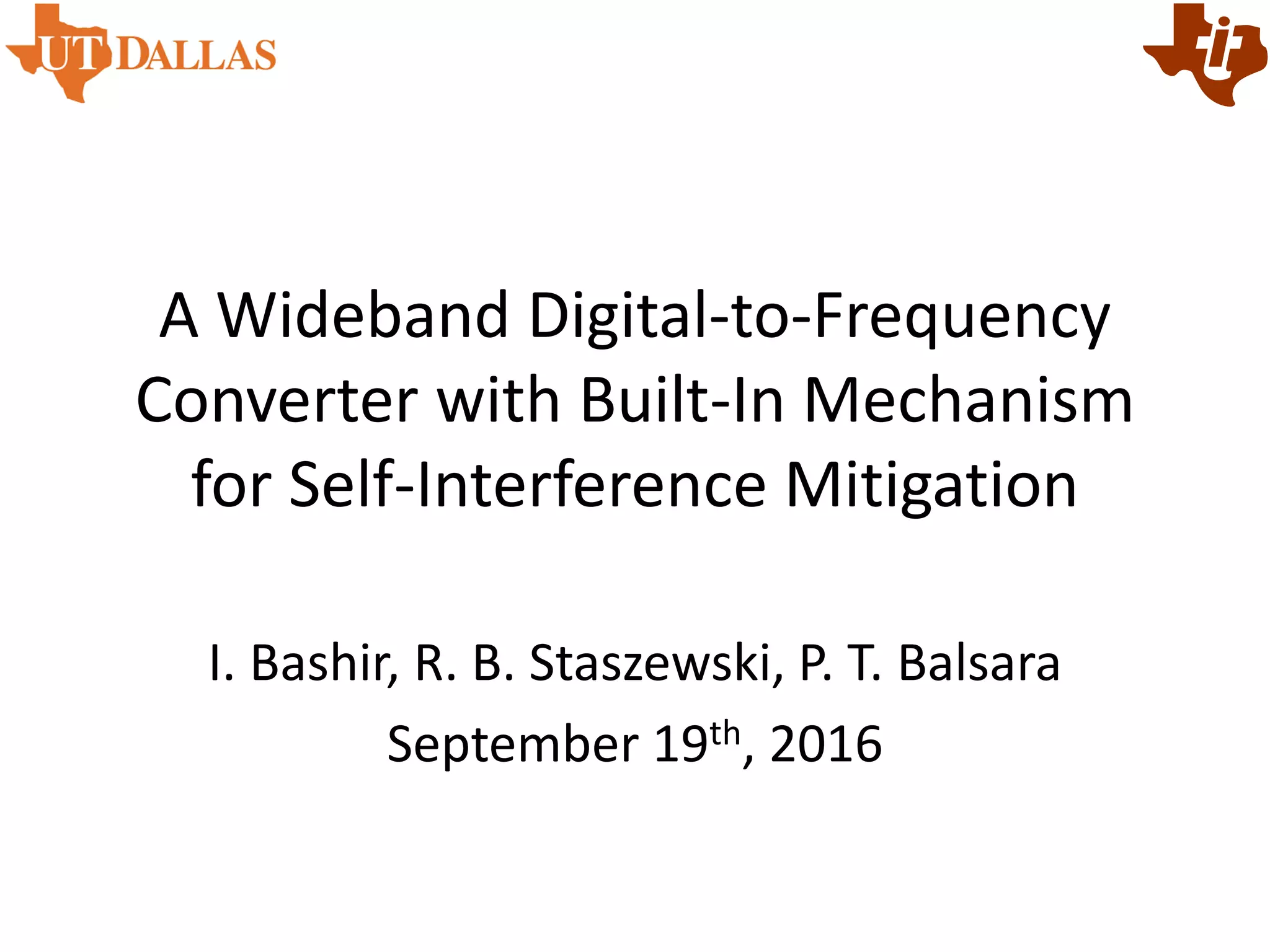
![Problem Statement
The ΣΔ dithering process also
creates an interference signal at
DCO resonance frequency. This
signal creates injection pulling in
the DCO and can limit the
modulation accuracy of the
transmitter. The amplitude of the
injected signal and therefore the
extent of the parasitic FM due to
injection pulling is a function of the
fractional portion of the oscillator’s
tuning word dT
f. The graphical
representation of the interference
mechanism is shown in the figure.
dT
f =0.25
f
Magnitude
fo
Iinj
fΣΔ=fo/2
DCO LC Tank
Selectivity
dT
f =0.75
f
Magnitude
fo
Iinj
fΣΔ=fo/2
DCO LC Tank
Selectivity
(a)
(b)
(c)
dTF
dTF
dT
f =0.50
f
Magnitude
fo
Iinj
fΣΔ=fo/2
DCO LC Tank
Selectivity
dTF
dT
f
Iinj
fΣΔ=fo/2
dT
f
Iinj
fΣΔ=fo/4
(d)
dT
f
Iinj
fΣΔ=fo/8
N=fo/fΣΔ
[3]](https://image.slidesharecdn.com/7883188e-4ea7-483b-a135-1651baa2a03b-160920075344/85/Bashir_09192016-4-320.jpg)
![Numerical Modeling
The ADPLL transfer function (TF) analysis in [2] is extended to include the
described impairment. The TF of the impairment Hcl,P has bandpass response
with respect to ωout. The integration operation from ωout to ϕN,P shapes the high-
pass TF into a bandpass TF.
(a)
+
-
Phase detector Normalized DCO
E
KDCO
Loop filter
s
ϕR
KDCO
fR
IIR
filter NTW
ϕ VE
n,TDC/2 OTW
ϕN,R N
fR
ϕN,V+ϕN,P
s
1
(b)
ϕN,R
Hcl,R
ϕN,V
Hcl,V
ϕN,TDC
Hcl,TDC
Hcl,P
+
Composite
ADPLL Phase
Noise Spectrum
fc
fc
fc
fc
ϕR,out ϕTDC,out
ϕV,out ϕP,out
ωout](https://image.slidesharecdn.com/7883188e-4ea7-483b-a135-1651baa2a03b-160920075344/85/Bashir_09192016-7-320.jpg)
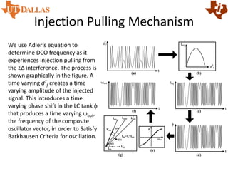
![Numerical Modeling
The model is simulated in time domain with a GMSK test vector
and the output spectrum is compared with measurement as shown
in the figure below. The distortion causes ‘spectral growth’ at
critical frequency offsets from the carrier such as 400 kHz.
10
5
10
6
10
7
-160
-150
-140
-130
-120
-110
-100
-90
-80
Frequency offset from carrier [Hz]
PhaseNoise[dBc/Hz]
R,out
TDC,out
V,out
P,out
Composite
1909.4 1909.6 1909.8 1910 1910.2
-80
-70
-60
-50
-40
-30
-20
-10
0
Frequency [MHz]
Power[dBm]/30kHz
Ideal
Simulated
Measured](https://image.slidesharecdn.com/7883188e-4ea7-483b-a135-1651baa2a03b-160920075344/85/Bashir_09192016-8-320.jpg)
![Proposed Solution
An effective solution is to manipulate the phase of the aggressor such
that the impact of this impairment is minimized. This operation
essentially tunes the parameter θ in the equation below to ~0⁰. The
phase adjustment is performance by adjusting the delay of the ΣΔ
sampling clock as shown in the ‘Self-Interference Mitigation Circuit’ in
the figure below.
OUT
017 m
DCO
DCO
Interface
Logic
CTBCTB
ΣΔ
÷N÷2
OSCP
OSCN
Self-Interference
Mitigation Circuit
τd
T
d
~
dTI
1-64
dTF
1-3
T
df
+
-
VDD
6 8
[3]](https://image.slidesharecdn.com/7883188e-4ea7-483b-a135-1651baa2a03b-160920075344/85/Bashir_09192016-9-320.jpg)
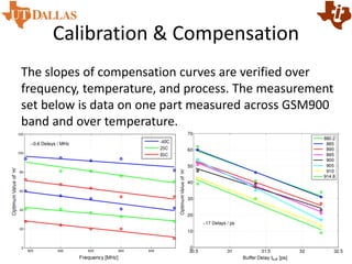
![Calibration & Compensation
The optimum delay code ‘m’
requires calibration and
compensation over frequency and
temperature. The calibration is
performed by measuring the
statistics of the phase error signal
of the ADPLL. As shown in Fig(b),
the worst delay setting is easily
distinguished and calibrated in a
particular frequency band. The
compensation adds an offset to
avoid the worst delay setting
using the equation:
Random data
CKV
m
DCO
ΣΔ
÷N ÷2τd
T
d 70.50
~
dTI
1-64
dTF
1-3
Phase
Detector
E[k]
Loop Filter
(PHE) (Filtered PHE)
Processor T
df
(a)
(b)](https://image.slidesharecdn.com/7883188e-4ea7-483b-a135-1651baa2a03b-160920075344/85/Bashir_09192016-10-320.jpg)
![References
• http://www.researchgate.net/profile/Imran_Bashir5
– “A Wideband Digital-to-Frequency Converter with Built-In
Mechanism for Self-Interference Mitigation”
– “Mitigation of RF Oscillator Pulling through Adjustable Phase
Shifting”
• [1] C.-M. Hung, et. al, "A first RF digitally-controlled oscillator for SAW-
less TX in cellular systems," Proc. Of 2005 Symposium of VLSI Circuits, pp.
402-405, June 2005.
• [2] Staszewski RB (2006) All digital frequency synthesizer in deep submicron
CMOS. Wiley, New Jersey.
• [3] I. Bashir, R. B. Staszewski, O. E. Eliezer, and P. T. Balsara “A wideband
digital-to-frequency converter with built-In mechanism for self-interference
mitigation ,” Journal of Electronic Testing (JETTA): Theory and Applications;
Special Issue on Analog, Mixed-Signal and RF Testing, vol. 32, no. 4, pp.
437–445, Aug. 2016](https://image.slidesharecdn.com/7883188e-4ea7-483b-a135-1651baa2a03b-160920075344/85/Bashir_09192016-12-320.jpg)

![Multiband Transceivers - [Chapter 4] Design Parameters of Wireless Radios](https://cdn.slidesharecdn.com/ss_thumbnails/ch4-150613070934-lva1-app6892-thumbnail.jpg?width=640&height=640&fit=bounds)
![RF Module Design - [Chapter 3] Linearity](https://cdn.slidesharecdn.com/ss_thumbnails/rfch3-150613070345-lva1-app6891-thumbnail.jpg?width=640&height=640&fit=bounds)

![RF Module Design - [Chapter 7] Voltage-Controlled Oscillator](https://cdn.slidesharecdn.com/ss_thumbnails/rfch7-150613070347-lva1-app6892-thumbnail.jpg?width=640&height=640&fit=bounds)
![RF Module Design - [Chapter 1] From Basics to RF Transceivers](https://cdn.slidesharecdn.com/ss_thumbnails/rfch1-150613070344-lva1-app6892-thumbnail.jpg?width=640&height=640&fit=bounds)


![射頻電子 - [第六章] 低雜訊放大器設計](https://cdn.slidesharecdn.com/ss_thumbnails/ch6-150613065106-lva1-app6892-thumbnail.jpg?width=640&height=640&fit=bounds)
![RF Module Design - [Chapter 5] Low Noise Amplifier](https://cdn.slidesharecdn.com/ss_thumbnails/rfch5-150613070346-lva1-app6891-thumbnail.jpg?width=640&height=640&fit=bounds)
![Multiband Transceivers - [Chapter 7] Multi-mode/Multi-band GSM/GPRS/TDMA/AMP...](https://cdn.slidesharecdn.com/ss_thumbnails/ch7-150613070936-lva1-app6892-thumbnail.jpg?width=640&height=640&fit=bounds)
![Multiband Transceivers - [Chapter 1]](https://cdn.slidesharecdn.com/ss_thumbnails/ch1-150613070932-lva1-app6891-thumbnail.jpg?width=640&height=640&fit=bounds)

![RF Circuit Design - [Ch4-1] Microwave Transistor Amplifier](https://cdn.slidesharecdn.com/ss_thumbnails/ch4-1-150613064409-lva1-app6892-thumbnail.jpg?width=640&height=640&fit=bounds)
![Agilent ADS 模擬手冊 [實習1] 基本操作與射頻放大器設計](https://cdn.slidesharecdn.com/ss_thumbnails/1adsbasics-150613072812-lva1-app6891-thumbnail.jpg?width=640&height=640&fit=bounds)

![Agilent ADS 模擬手冊 [實習2] 放大器設計](https://cdn.slidesharecdn.com/ss_thumbnails/2adsamp-150613072818-lva1-app6892-thumbnail.jpg?width=640&height=640&fit=bounds)
![射頻電子 - [第三章] 史密斯圖與阻抗匹配](https://cdn.slidesharecdn.com/ss_thumbnails/ch3-150613065103-lva1-app6892-thumbnail.jpg?width=640&height=640&fit=bounds)
![射頻電子 - [第二章] 傳輸線理論](https://cdn.slidesharecdn.com/ss_thumbnails/ch2-150613065059-lva1-app6891-thumbnail.jpg?width=640&height=640&fit=bounds)


![射頻電子 - [第一章] 知識回顧與通訊系統簡介](https://cdn.slidesharecdn.com/ss_thumbnails/ch1-150613065058-lva1-app6891-thumbnail.jpg?width=640&height=640&fit=bounds)
![RF Circuit Design - [Ch1-2] Transmission Line Theory](https://cdn.slidesharecdn.com/ss_thumbnails/ch1-2-150613064349-lva1-app6892-thumbnail.jpg?width=640&height=640&fit=bounds)
![射頻電子 - [第四章] 散射參數網路](https://cdn.slidesharecdn.com/ss_thumbnails/ch4-150613065103-lva1-app6891-thumbnail.jpg?width=640&height=640&fit=bounds)
![RF Circuit Design - [Ch3-2] Power Waves and Power-Gain Expressions](https://cdn.slidesharecdn.com/ss_thumbnails/ch3-2-150613064404-lva1-app6891-thumbnail.jpg?width=640&height=640&fit=bounds)
![RF Circuit Design - [Ch2-2] Smith Chart](https://cdn.slidesharecdn.com/ss_thumbnails/ch2-2-150613064401-lva1-app6891-thumbnail.jpg?width=640&height=640&fit=bounds)

![RF Module Design - [Chapter 6] Power Amplifier](https://cdn.slidesharecdn.com/ss_thumbnails/rfch6-150613070347-lva1-app6891-thumbnail.jpg?width=640&height=640&fit=bounds)


![Agilent ADS 模擬手冊 [實習3] 壓控振盪器模擬](https://cdn.slidesharecdn.com/ss_thumbnails/3adsosc-150613072819-lva1-app6892-thumbnail.jpg?width=640&height=640&fit=bounds)