Download to read offline
![IXYS Corporation; 3540 Bassett Street; Santa Clara, CA 95054; Tel: 408-982-0700; Fax: 408-496-0670
IXYS Semiconductor GmbH; Edisonstr. 15; D-68623; Lampertheim, Germany; Tel: +49-6206-503-0; Fax: +49-6206-503627
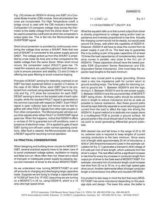
3
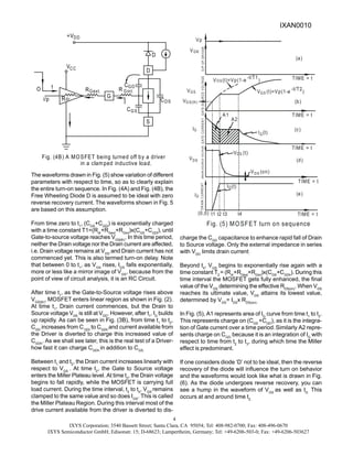
Voltage). The graph has a slope ( ID
/ VGS
) equal to gm
,
which is called transconductance. Please note that the
actual relationship between VGS
and ID
is shown by dotted
line and it can be observed that in the vicinity of VGS(th)
, the
relationship between VGS
and ID
is parabolic in nature:
ID
= K [VGS
-VGS(th)
]2
Eq.1.1
However, for Power MOSFETs, it is appropriate to con-
sider the relationship to be linear for values of VGS
above
VGS(th).
The manufacturer’s data sheet value of VGS(th)
is speci-
fied at 25
o
C.
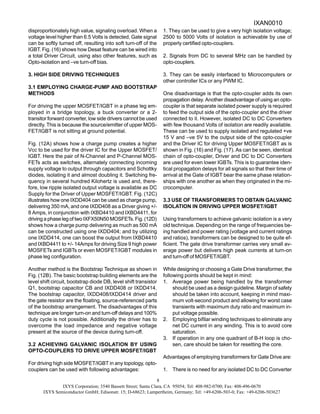
Fig. (3A) shows a symbol of N-Channel MOSFET and an
equivalent model of the same with three inter-junction para-
sitic capacitances, namely: CGS
, CGD
and CDS
. I have shown
all these as variable as they indeed are. For example the
CGD
, decreases rapidly as the Drain to Source voltage rises,
as shown in Fig. (3B). In Fig. (3B), the high value of CGD
is
called CGDh
, while the low value of CGD
is termed CGDl.
Fig.
(1B) shows another cross-sectional view of a MOSFET
with all these capacitances. In addition, It also shows the
internal body diode and the parasitic BJT.
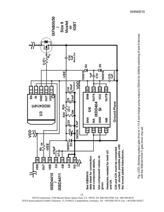
1.3 Turn-on and Turn-off Phenomena
1.3.1 Turn-on Phenomenon
TounderstandTurn-onandTurn-offphenomenaofthePower
MOSFET, we will assume clamped inductive switching as
it is the most widely used mode of operation. This is shown
in Fig. (4A) and Fig. (4B). A model of MOSFET is shown
with all relevant components, which play a role in turn-on
and turn-off events. As stated above, MOSFET’s Gate to
Source Capacitance CGS
needs to be charged to a critical
voltage level to initiate conduction from Drain to Source. A
few words of explanation will help understand Fig. (4A)
and Fig. (4B). The clamped inductive load is being shown
by a current source with a diode D connected antiparallel
across the inductor. The MOSFET has its intrinsic internal
Gate resistance, called RGint
. As described above, the in-
ter-junction parametric capacitances (CGS
, CGD
and CDS
)
are shown and connected at their proper points. VDD
repre-
sents the DC Bus voltage to the Drain of the MOSFET
through the clamped inductive load. The Driver is supplied
by Vcc of value Vp and its ground is connected to the
common ground of VDD
and is returned to the Source of
the MOSFET. The output from the Driver is connected to
the Gate of the MOSFET through a resistor RGext
.
Now when a positive going pulse appears at the input ter-
minal of the Driver, an amplified pulse appears at the out-
put terminal of the Driver with an amplitude Vp. This is fed
to the Gate of the MOSFET through RGext
. As one can see
the rate of rise of voltage, VGS
, over Gate and Source termi-
nals of the MOSFET is governed by value of the total resis-
tance in series (Rdr
+RGext
+RGint
) and total effective value of
capacitance (CGS
+CGD
). Rdr
stands for the output source
impedance of the Driver. Rgext
is the resistance one gener-
ally puts in series with the Gate of a MOSFET to control
the turn-on and turn-off speed of the MOSFET.
Fig. (3A) Symbol and equivalent circuit of a MOSFET
Symbol of
N-Channel MOSFET
D
G
S
G
CGD
GS
C
G
R
D
S
CDS
RDS(on)
int
V DS
GS
V
Fig. (3B) C variation V
with respect to DS
DS
V =
GD
C
GD
C
CGD
h
l
GD
Fig (4A) A MOSFET being turned on by a driver
in a clamped inductive load.
Gext.
O
t
i/p R
o/p
DRIVER
dr
G
I
R
V
+V
CC
DD
GD
GS
G
C
Gs
Gint.
I
R
S
C
C
IGD
D
D
DS
IXAN0010](https://image.slidesharecdn.com/ixan0010driversigbt-210504182638/85/Ixan0010-drivers-igbt-3-320.jpg)


This document provides an overview of MOSFET and IGBT driver theory and applications. It discusses MOSFET and IGBT technology, critical MOSFET parameters like gate capacitances, and turn-on and turn-off phenomena. It describes types of drivers, isolation techniques, IXYS's line of MOSFET/IGBT drivers, and practical considerations for applying drivers. The document aims to assist both experienced and new designers in understanding practical aspects of driving power devices in different circuit configurations.