The document describes experiments to be performed in a Power Electronics lab. It includes experiments to study the switching characteristics of power electronics devices like MOSFETs and IGBTs. The experiments aim to determine timing parameters for switching such as turn-on delay, rise time, turn-off delay and fall times by applying gate pulses and observing the drain/collector current waveforms. Circuits are provided to test MOSFETs and IGBTs and procedures describe how to connect equipment and measure the switching parameters.


![=
1
TON V dt +
T
0 dt
T 0 in
TON
1
[V ] [t]
TON
T in 0
V
in
T
*TON
T
V V * ON
(2)
o,avg in T
where T = Chopping period and
TON
T
= Duty cycle ratio
From Eqn. 2, it is clear that the average output voltage Vo,avg depends on the TON and T.
It can be varied by varying either the chopping frequency (f) or by varying TON. Thus the power
flow in the circuit can be controlled.
The switch shown in Fig.3, can be any one of the following power semiconductor
devices: i) SCR, ii) power transistor (power-BJT), iii) power-MOSFET, iv) IGBT and v) GTO.
In this experiment, IGBT [Insulated Gate Bipolar Junction Transistor] is used as a switch.
PRECAUTIONS
1. Ensure the switch is in OFF position while doing circuit connection.
2. Ensure pulse release switch in OFF position whenever power is switched ON.
EXPERIMENTAL PROCEDURE
I) Fixed Frequency Variable Time Ratio Control (FFVTRC)
1. Connect the load and the device as shown is Fig.(3a).
2. Connect channel-1 of CRO and ground across the load (R), to measure the output
voltage. Connect Channel-2 of CRO to measure the input voltage (Vin) as shown in Fig.
(3a).
3. Fix the carrier frequency knob at one position and adjust TON and TOFF as given
in Table 1.
19
Print to PDF without this message by purchasing novaPDF (http://www.novapdf.com/)](https://image.slidesharecdn.com/b-151222155313/85/B-e-vi-semester-power-electronics-lab-20-320.jpg)


![o
PROCEDURE FOR MODE1
(i) Give connections as per the circuit diagram shown in Fig.5 and Fig.6.
(ii) Provide the switch SW2 in “INT” mode.
(iii) Keep the firing knob in minimum position.
(iv) Switch ON the trainer power module.
(v) Switch ON the power circuit switch SW4.
(vi) Release the pulse through pulse release (PR) switch SW3.
(vii) Vary the control voltage (firing angle) from 0 to 180 degrees in steps of 30.
(viii) Note down the DC average output voltage for each step using DMM.
(ix) Trace the output voltage waveform from CRO.
(x) Calculate the firing angle from the waveform obtained.
Compare the theoretical and practical values of Vo obtained for various α and
tabulate in Table1.
Formula for obtaining average dc output voltage with resistive load
Average DC output voltage V =
2 *Vin *[1+cosα]
π
where
Vin = RMS value of AC input voltage = 24 volts.
= Firing angle in degrees (0
to 180
) = (180*t)/T
t = triggering time
T= total time for one half cycle.
Specimen calculation for output voltage
For = 45
Vo
2*24[1+cos45o
]
3.14
= 18.45 V
39
Print to PDF without this message by purchasing novaPDF (http://www.novapdf.com/)](https://image.slidesharecdn.com/b-151222155313/85/B-e-vi-semester-power-electronics-lab-40-320.jpg)


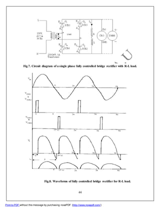
![o
Mode 2: Operation with resistive and inductive loads
Bridge rectifier operated with resistive and inductive loads is shown in Fig.7.
Working principle is same as explained in mode1 except that during positive half cycle of
AC input voltage SCR1 and SCR2 will continue to conduct beyond ωt = π due to
inductive load even though the supply voltage reverse its polarity in the negative half
cycle. Due to this, the load current will reach zero only at π+β where β is known as
extinction angle. SCR1 and SCR2 turn OFF by current commutation. Similarly during
negative half cycle of AC input voltage, SCR3 and SCR4 will continue to conduct
beyond ωt = 2π due to inductive load even though the supply voltage reverse its polarity
in the positive half cycle. The load current will reach zero only at 2π+β. SCR3 and SCR4
turns OFF by current commutation as before. Hence, the cycles repeat. The waveforms of
load current, load voltage and gating pulses are shown in Fig.8. The front panel
connection diagram for mode 2 is shown in Fig.9 and the procedure is as follows:
PROCEDURE FOR MODE2
(i) Give the connections as per Figs.7 and 9.
(ii) Repeat the mode1 procedure from steps (ii) to (x).
(iii) Calculate the extinction angle (β) from the waveform obtained.
(iv) Comparison of the theoretical and practical values of Vo are tabulated in Table. 2.
Formula for obtaining average dc output voltage with resistive and inductive loads
Average DC output voltage V =
2*Vin *[cosα-cosβ]
π
where
Vin = RMS value of AC input voltage = 24 V.
= Firing angle in degrees (0
to 180
)
= Extinction angle in degrees (0
to 180
)
43
Print to PDF without this message by purchasing novaPDF (http://www.novapdf.com/)](https://image.slidesharecdn.com/b-151222155313/85/B-e-vi-semester-power-electronics-lab-44-320.jpg)