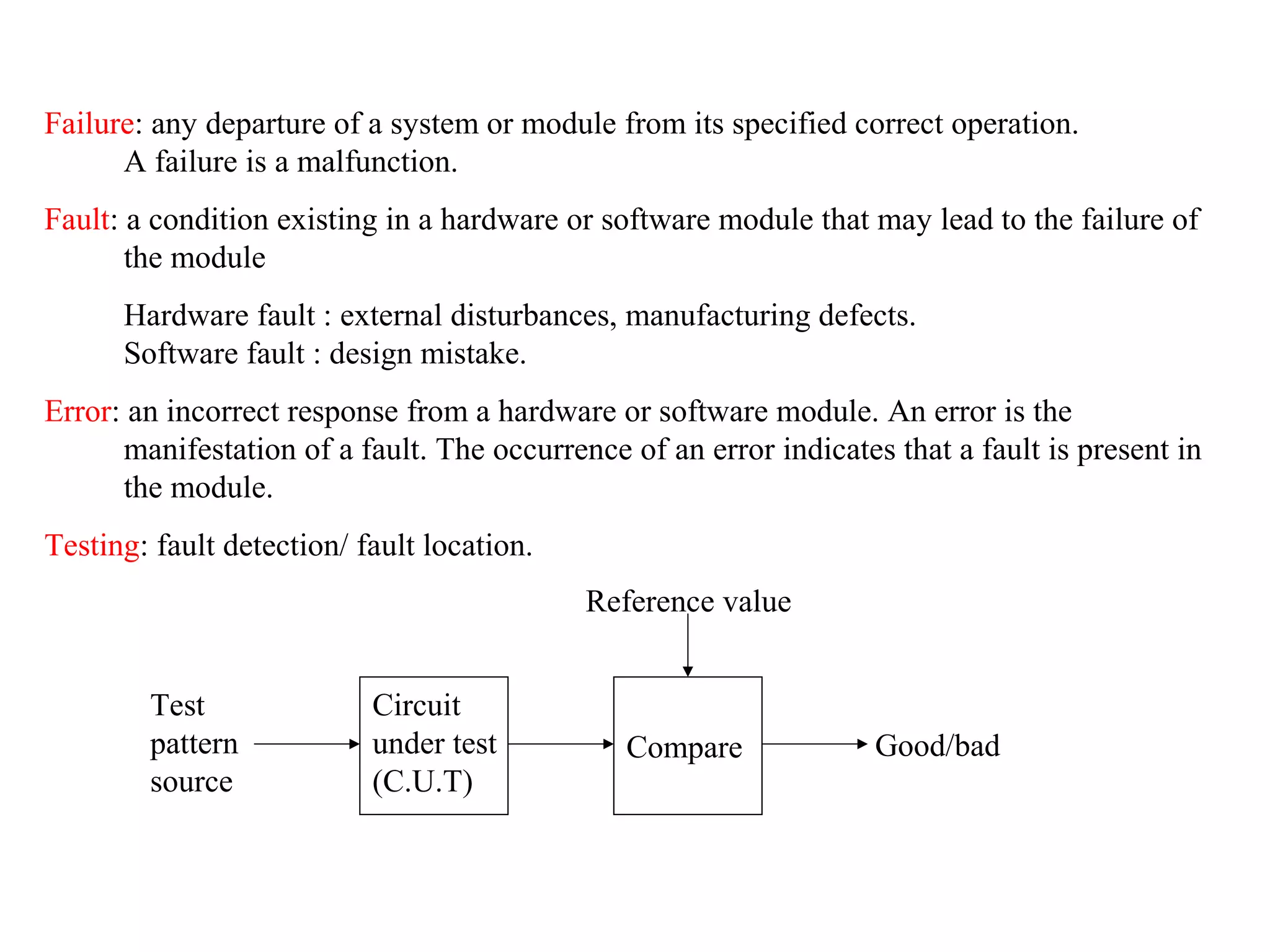
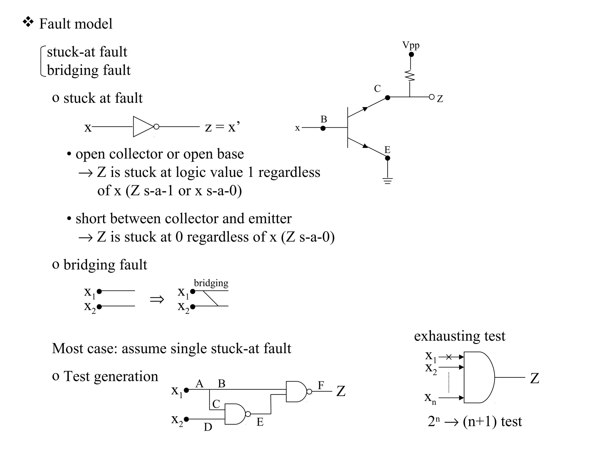
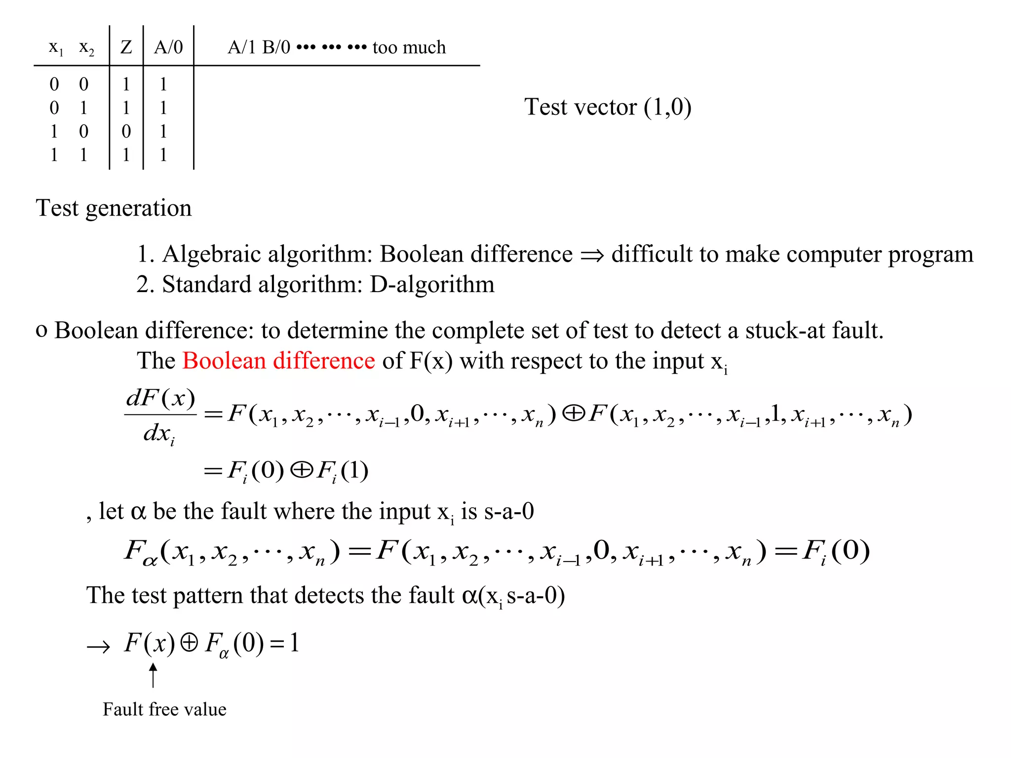
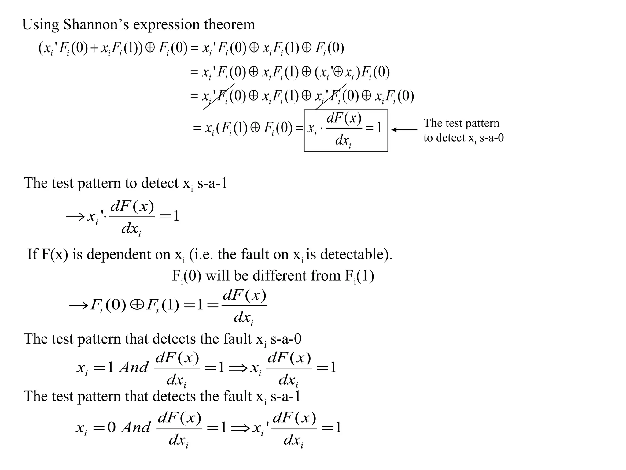
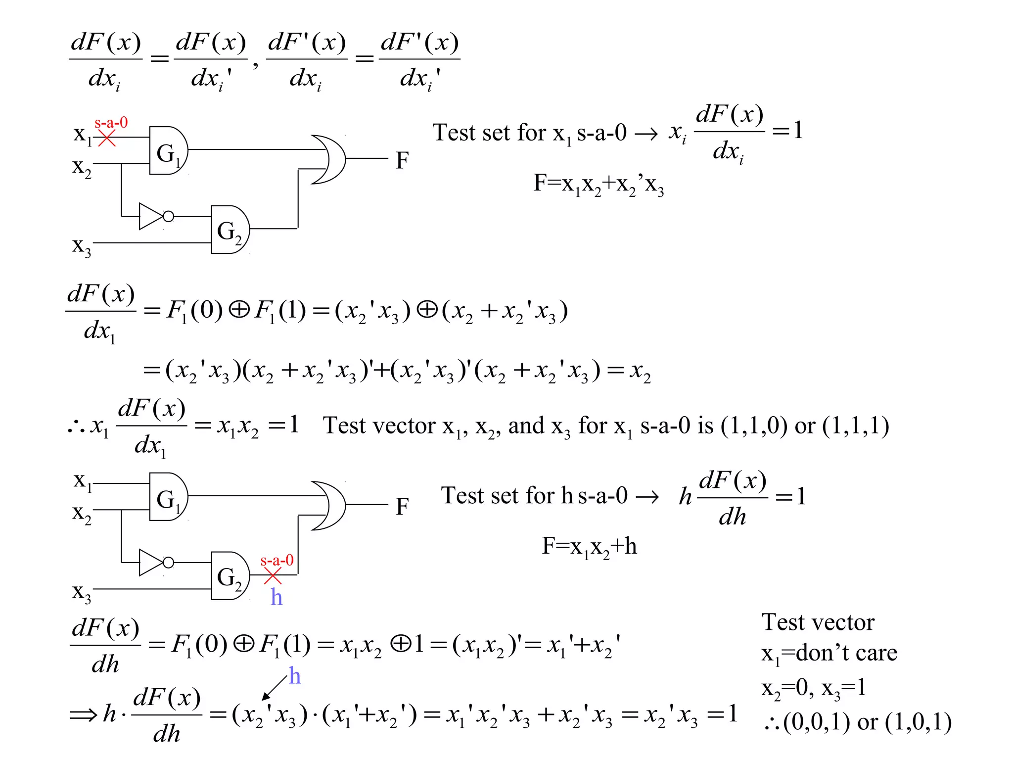
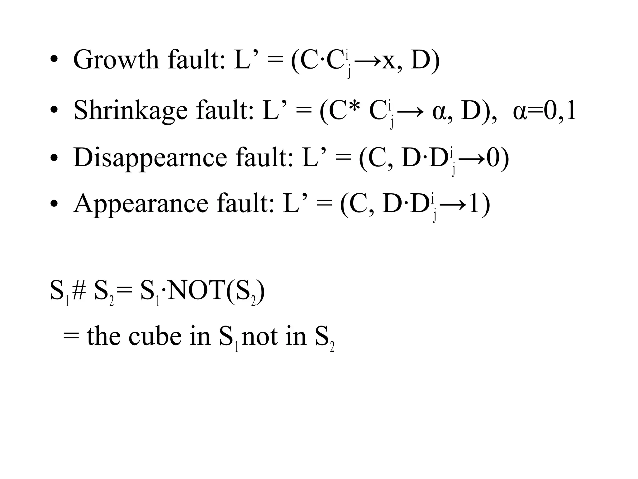
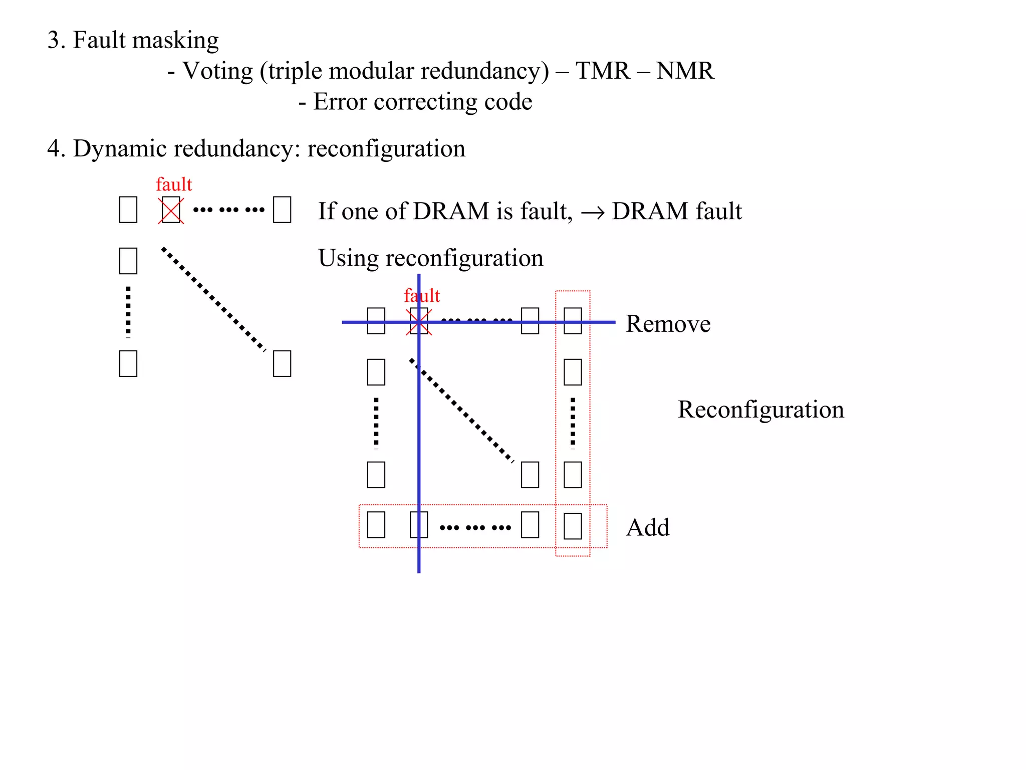
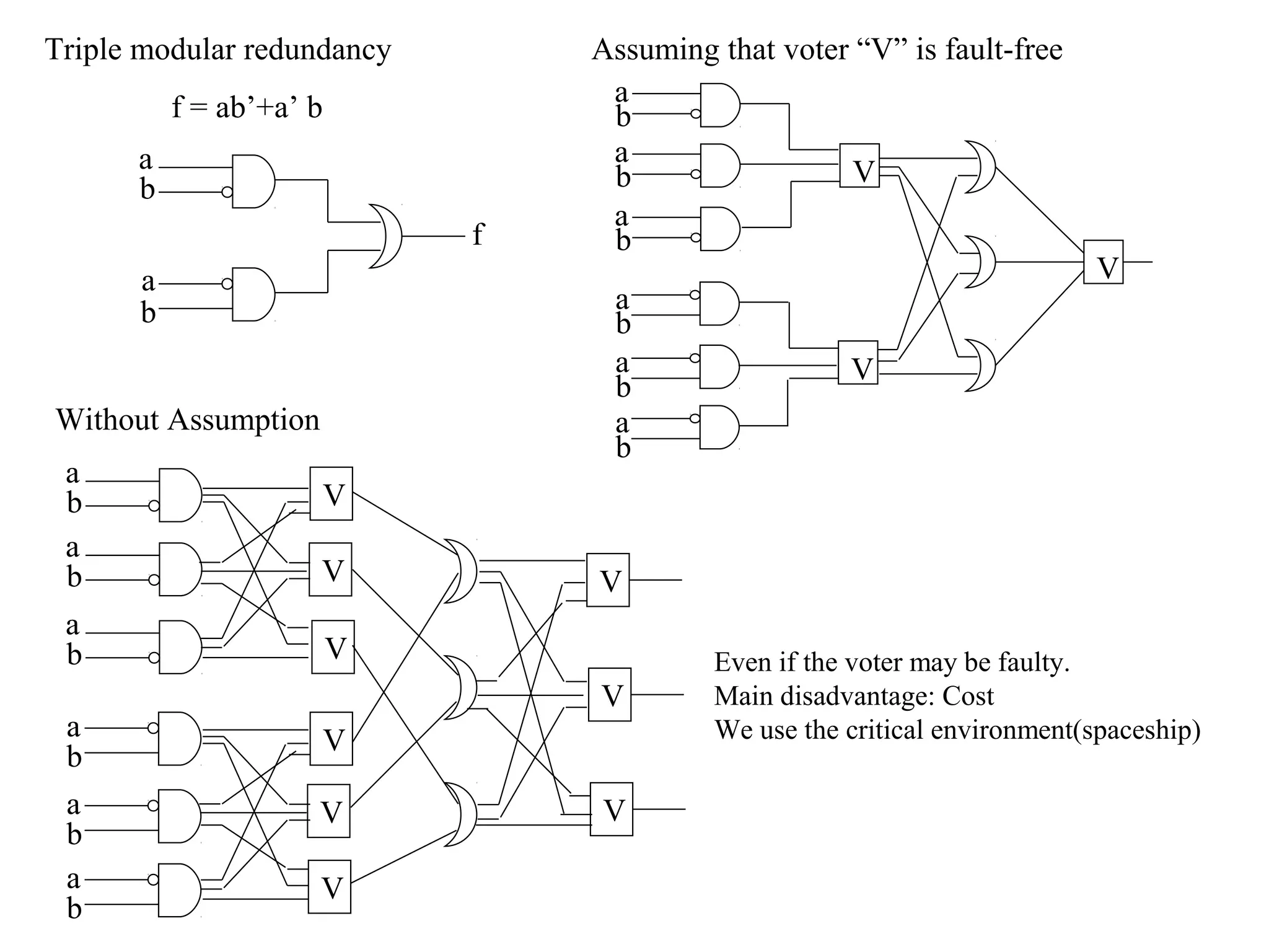
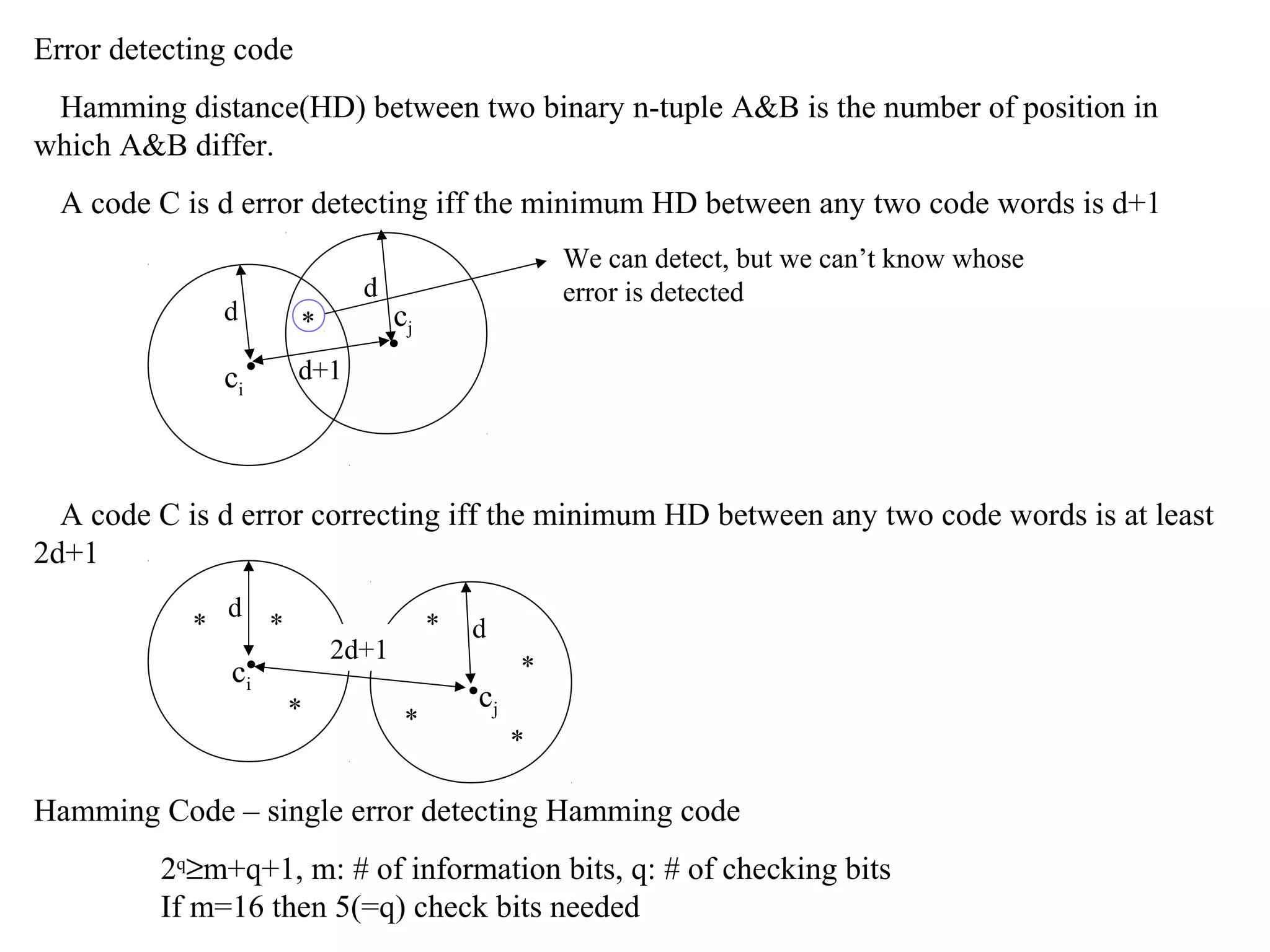
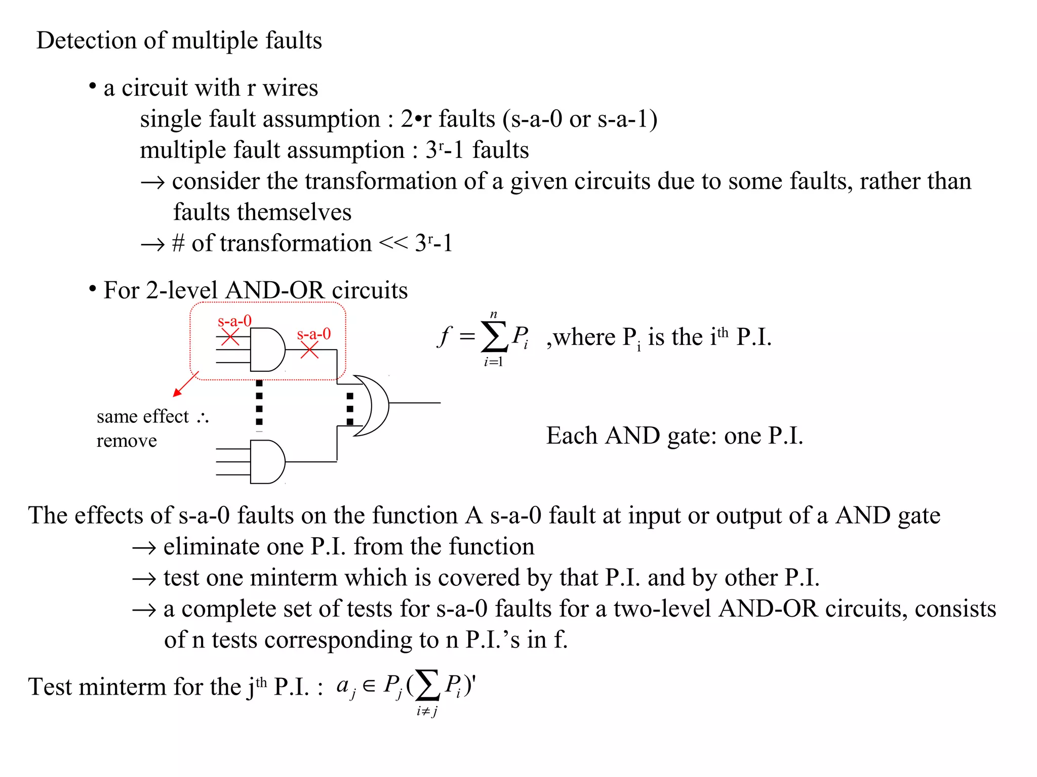
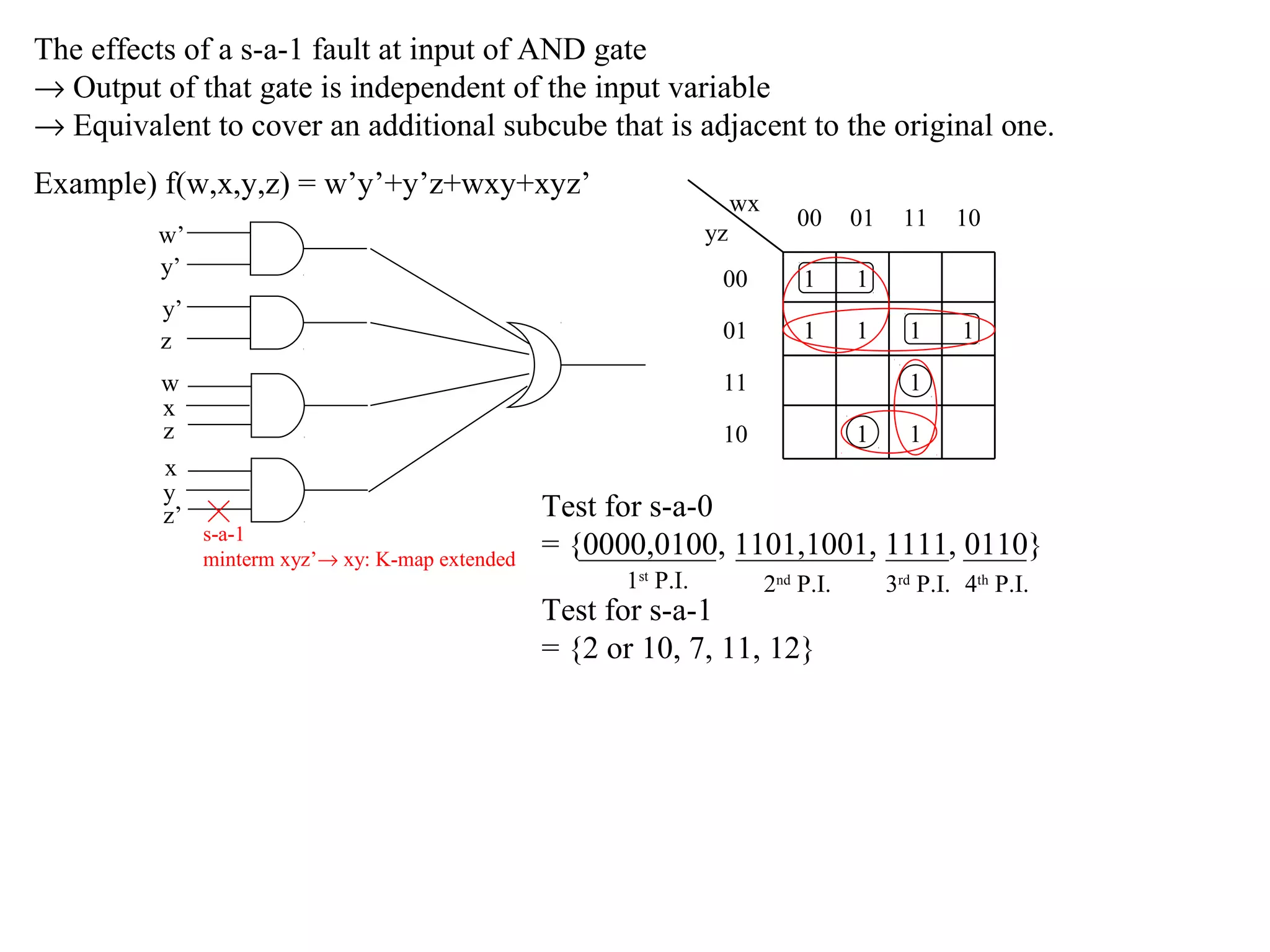
Chapter 7.
Testing of a digital circuit
Failure: any departure of a system or module from its specified correct operation.
A failure is a malfunction.
Fault: a condition existing in a hardware or software module that may lead to the failure of
the module
Hardware fault : external disturbances, manufacturing defects.
Software fault : design mistake.
Error: an incorrect response from a hardware or software module. An error is the
manifestation of a fault. The occurrence of an error indicates that a fault is present in
the module.
Testing: fault detection/ fault location.
Reference value
Test
pattern
source

Circuit
under test
(C.U.T)

Compare

Good/bad
 Fault model
Vpp

stuck-at fault
bridging fault
C

o stuck at fault
z = x’

x

Z

B

x

E

• open collector or open base
→ Z is stuck at logic value 1 regardless
of x (Z s-a-1 or x s-a-0)
• short between collector and emitter
→ Z is stuck at 0 regardless of x (Z s-a-0)
o bridging fault
x1
x2

⇒ x1
x2

bridging

exhausting test
x1
x2

Most case: assume single stuck-at fault
o Test generation

x1
x2

A

B

F

C
D

E

Z

xn
2n → (n+1) test

Z
x1 x2

Z

A/0

0
0
1
1

1
1
0
1

1
1
1
1

0
1
0
1

A/1 B/0 ••• ••• ••• too much

Test vector (1,0)

Test generation
1. Algebraic algorithm: Boolean difference ⇒ difficult to make computer program
2. Standard algorithm: D-algorithm
o Boolean difference: to determine the complete set of test to detect a stuck-at fault.
The Boolean difference of F(x) with respect to the input xi
dF ( x )
= F ( x1 , x2 ,  , xi −1 ,0, xi +1 ,  , xn ) ⊕ F ( x1 , x2 ,  , xi −1 ,1, xi +1 ,  , xn )
dxi
= Fi (0) ⊕ Fi (1)
, let α be the fault where the input xi is s-a-0

Fα ( x1 , x2 ,  , xn ) = F ( x1 , x2 ,  , xi −1 ,0, xi +1 ,  , xn ) = Fi (0)
The test pattern that detects the fault α(xi s-a-0)
→ F ( x) ⊕ Fα (0) = 1
Fault free value
Using Shannon’s expression theorem
( xi ' Fi (0) + xi Fi (1)) ⊕ Fi (0) = xi ' Fi (0) ⊕ xi Fi (1) ⊕ Fi (0)
= xi ' Fi (0) ⊕ xi Fi (1) ⊕ ( xi '⊕ xi ) Fi (0)
= xi ' Fi (0) ⊕ xi Fi (1) ⊕ xi ' Fi (0) ⊕ xi Fi (0)
dF ( x)
= xi ( Fi (1) ⊕ Fi (0) = xi ⋅
=1
dxi
The test pattern to detect xi s-a-1
dF ( x)
→ xi '⋅
=1
dxi
If F(x) is dependent on xi (i.e. the fault on xi is detectable).
Fi(0) will be different from Fi(1)
dF ( x)
→ Fi (0) ⊕ Fi (1) = 1 =
dxi
The test pattern that detects the fault xi s-a-0
dF ( x)
dF ( x)
xi = 1 And
= 1 ⇒ xi
=1
dxi
dxi
The test pattern that detects the fault xi s-a-1
dF ( x)
dF ( x )
xi = 0 And
= 1 ⇒ xi '
=1
dxi
dxi

The test pattern
to detect xi s-a-0
dF ( x) dF ( x) dF ' ( x) dF ' ( x)
=
,
=
dxi
dxi '
dxi
dxi '
x1 s-a-0
x2
x3

G1

F

Test set for x1 s-a-0 → xi

dF ( x)
=1
dxi

F=x1x2+x2’x3

G2

dF ( x)
= F1 (0) ⊕ F1 (1) = ( x2 ' x3 ) ⊕ ( x2 + x2 ' x3 )
dx1
= ( x2 ' x3 )( x2 + x2 ' x3 )'+( x2 ' x3 )' ( x2 + x2 ' x3 ) = x2

dF ( x)
= x1 x2 = 1 Test vector x1, x2, and x3 for x1 s-a-0 is (1,1,0) or (1,1,1)
dx1
x1
dF ( x)
Test set for h s-a-0 → h
=1
G1
F
x2
dh
F=x1x2+h
s-a-0
G2
x3
h
Test vector
dF ( x)
= F1 (0) ⊕ F1 (1) = x1 x2 ⊕1 = ( x1 x2 )' = x1 '+ x2 '
x1=don’t care
dh
h
x2=0, x3=1
dF ( x)
⇒h⋅
= ( x2 ' x3 ) ⋅ ( x1 '+ x2 ' ) = x1 ' x2 ' x3 + x2 ' x3 = x2 ' x3 = 1 ∴(0,0,1) or (1,0,1)
dh

∴ x1
Disadv. of Boolean difference;
Difficult to manipulate algebraic equation.
method generates all test inputs for a given fault.
require a large quantity of time and memory
Test generation algorithm based on path sensitization
Two problems in test generation procedure
Creation of a change at the faulty line.
Propagation of the change to the primary output line.

1.
2. This
→

1.
2.

The basic principles of single-path sensitization
At the site of the fault, assign a logical value complementary to the fault being tested.
Select a path from the primary inputs through the site of the fault to a primary
output → forward sensitizing (apply 1’s to all remaining inputs to the AND and
NAND gates in the path, and 0’s to the OR and NOR gates in the path).
Determine the primary inputs that will produce all the necessary signal values →
backward tracing or line justification.
Example) Find a test vector!
x1
x2
x3
x4

s-a-0

1.
2.
3.
Example) Find a test vector!
G4
G1
x1
x2
x3
x4

G2

s-a-1

G5
G8
G6

G3
G7
We can’t find a test vector using a single-path sensitization. Is there no test vector? Ans)
we don’t know. We can try to use multiple-path sensitization = D – algorithms.

Multiple path sensitization
D-algorithm; 1966 Roth(IBM) – five logic values used : 0, 1, X , D (1 / 0), D (0 / 1)
• Singular cube: The singular cover of a gate is a compact truth table representation in
terms of the {0,1,X} variables. Each row of the singular
cover is
called a singular cube.
1
2

3

1 2 3
1 1 1
0 X 0
X 0 0

Compact
truth table

• A primitive D-cube(PDC) of a fault: minimal specification of inputs to set D or D
at the output of a faulty gate.
1
2
3

s-a-1

4

1 2 3
0 1 1

4
D(0/1)

• Propagation D-cube: minimal specification of inputs to the gate such that a D or D
on an input (inputs) is propagated to its output as D or D
1
2
3

4

∩ 0 1 X D D
0
1
X
D
D

0
φ
0
φ
φ

φ
1
1
φ
φ

φ
φ
D
D
D λ

0
1
X
D

φ
φ

D
λ
D

φ : inconsistent
λ : may be possible

1 2 3 4
D 1 1 D
D Just replace to D
1 D 1
D
1 1 DD
D
D 1 D
D 1 D
D
1 D DD
D D D
with another choice of propagation
D

D-cube
Consider the process of generating a test for line 5/0 in fig 1.4.8. We start with the
following cube, which includes the primitive D-cube of failure for this fault:

The next step is to propagate this D farther toward line 11. Referring to propagation Dcubes in table 1.4.1, cube j shows that the D in cube k is automatically propagated to lines
6 and 7. Consider now the propagation along the path 6, 9, 11. Table 1.4.1 again shows
that the D on line 6 can be moved to line 9 by using cube d. In other words, a new cube
can be obtained by combining cubes d and k. This process of combination is referred to as
D-cube intersection.

Lines 7 and 9 now contain the change, which can be propagated further into line 11.
The next step is determine a value for the primary input line 4 since that is the only line
that has not been assigned a value. To create a 0 in line 10, both lines 7 and 8 must be a 1;
however, in cube m, line 7 is a D, indicating that cube m cannot result in a test vector along
5, 6, 9, 11. Start again from cube k to propagate along the path 5, 7, 10, 11. This leads to
the following cube:

The values of 1 and 4 are required to complete the operation. The resulting cube are
completing lines 1 and 4 is:
• D-frontier: The set of all gates whose output values are unspecified, but whose input
has some signal D or D
G4
G1

G2

3

G5

9

5

1
2

8

s-a-1

G8

6

G6
G3

1 2 3 4 5 6 7 8 9 10 11 12

10

G7

4

12

11

7

D-frontier

1 1 1 x 0 Dx 1 D x x x
1
1 D 1 1 D

G8,G6
Out, G6

G5,G6

1 1 1 x 0 Dx 1 D 1 1 D
1 x
0
1

Out, G6

1 1 1 x x Dx x D x x x
1 1 0

G8,G6

1 1 1 x 0 D0 1 D 1 1 D
1 1 1
0

Out, G6

1 1 1 x 0 Dx x D x x x
1 x
0
1

G8,G6

1 1 1 1 0 D0 1 D 1 1 D
1
1 1
0
conflict

x x x x x x x x x x x x
1 1 1 D
x 1 1 x x Dx x x x
1
D
D

x x
When conflict occurs, we have to go back to the previous D-frontier
1 2 3 4 5 6 7 8 9 10 11 12

D-frontier

1 1 1
1
1
1 1 1
x
1
1 1 1
1 1

x 0 Dx 1 D x x x
1 D D D

G8,G6

x 0 Dx 1 D D 1 D
1
x
0

Out, G6

x 0 D0 1 D D 1 D
1
1

Out, G6

1 1 1 1 0 D 0 1 D D 1 D G8,G6
1
Test vector

D-algorithm will derive a test for any fault if such a test exists
Detection of Faults in PLA
•

PLA characteristic
1. In a circuit structure, PLA essentially has only two levels of gates.
2. A more general fault model is necessary because of the way PLA is fabricated.

Fault Model: incorrect logical connections in the AND and OR plane
• Growth (G) fault: a connection in the AND plane is missing -> causing the
implicant to grow
• Disappearance (D) fault: a connection in the OR plane is missing -> causing the
implicant to disappear
• Shrinkage (S) fault: an intended connection in the AND plane is made -> causing
the implicant to shrink
• Apperance (A) fault: an intended connection in the OR plane is made -> causing
the implicant to appear
Single fault assumption: Important calsses of multiple faults are detected by any
single fault test set.
• Growth fault: L’ = (C·Cij →x, D)
• Shrinkage fault: L’ = (C* Cij → α, D), α=0,1
• Disappearnce fault: L’ = (C, D·Dij →0)
• Appearance fault: L’ = (C, D·Dij →1)
S1 # S2 = S1·NOT(S2)
= the cube in S1 not in S2
• Classification of fault-tolerant technique
1. Fault avoidance
- Environmental (dust free)
- High quality components
- Quality control
2. Fault detection: make sure the system is
working or not
- Duplication
- Error detection code: parity bit
- Self-checking
- Watchdog processor
3. Fault masking
- Voting (triple modular redundancy) – TMR – NMR
- Error correcting code
4. Dynamic redundancy: reconfiguration
fault
••• ••• •••

If one of DRAM is fault, → DRAM fault
Using reconfiguration
fault
••• ••• •••

Remove
Reconfiguration

••• ••• •••

Add
Triple modular redundancy
f = ab’+a’ b
a
b
f
a
b

Assuming that voter “V” is fault-free
a
b
a
V
b
a
b
a
b
a
b
a
b

Without Assumption
a
b
a
b

V

a
b

V

a
b
a
b
a
b

V

V

V
V
V
V
V
V

V

Even if the voter may be faulty.
Main disadvantage: Cost
We use the critical environment(spaceship)
Error detecting code
Hamming distance(HD) between two binary n-tuple A&B is the number of position in
which A&B differ.
A code C is d error detecting iff the minimum HD between any two code words is d+1
d

d

*

ci •

d+1

We can detect, but we can’t know whose
error is detected

cj
•

A code C is d error correcting iff the minimum HD between any two code words is at least
2d+1
*

d

c•
i

*

*

2d+1
*

*

d

•cj

*
*

Hamming Code – single error detecting Hamming code
2q≥m+q+1, m: # of information bits, q: # of checking bits
If m=16 then 5(=q) check bits needed
Detection of multiple faults
• a circuit with r wires
single fault assumption : 2•r faults (s-a-0 or s-a-1)
multiple fault assumption : 3r-1 faults
→ consider the transformation of a given circuits due to some faults, rather than
faults themselves
→ # of transformation << 3r-1
• For 2-level AND-OR circuits
s-a-0

n

f = ∑ Pi ,where Pi is the ith P.I.

s-a-0

i =1

same effect ∴
remove

Each AND gate: one P.I.

The effects of s-a-0 faults on the function A s-a-0 fault at input or output of a AND gate
→ eliminate one P.I. from the function
→ test one minterm which is covered by that P.I. and by other P.I.
→ a complete set of tests for s-a-0 faults for a two-level AND-OR circuits, consists
of n tests corresponding to n P.I.’s in f.
Test minterm for the jth P.I. : a j ∈ Pj (∑ Pi )'
i≠ j
The effects of a s-a-1 fault at input of AND gate
→ Output of that gate is independent of the input variable
→ Equivalent to cover an additional subcube that is adjacent to the original one.
Example) f(w,x,y,z) = w’y’+y’z+wxy+xyz’

wx

01

00

1

1

01

y’
z
w
x
z
x
y
z’

00

1

1

yz

w’
y’

10

1

1

1

11
1

10

s-a-1
minterm xyz’→ xy: K-map extended

11

1

Test for s-a-0
= {0000,0100, 1101,1001, 1111, 0110}
1st P.I.

2nd P.I.

Test for s-a-1
= {2 or 10, 7, 11, 12}

3rd P.I. 4th P.I.
Sequential Logic – Memory: Problems Generating a Test Sequence

● Initial state is unknown – controllability is required to set initial state.
● Fault signal must be propagated to primary outputs. Observability of final state is
required to check faulty state.

Scan Design: All flip-flops in a circuit are interconnected into one or more shift registers
and the content of the register is shifted in and out.
● Very few additional external connections used to access many internal nodes at
the cost of additional internal logic.
● All states completely observed and controlled form primary I/O.
Testing Procedure in scan-path design – LSSP

1)Scan in test vector Yj using Xn and TCK
2)Apply corresponding test vector on Xi inputs
3)After sufficient time for signals to propagate, check output Z.
4)Apply one clock pulse to SCK to enter new values of Yj into corresponding FFs.
5)Scan out with TCK and check Yj values.
Level-Sensitive – Level stays for a certain period.
Edge-Sensitive – Level only at pulse change.

4366 chapter7

  • 1.
    Chapter 7. Testing ofa digital circuit
  • 2.
    Failure: any departureof a system or module from its specified correct operation. A failure is a malfunction. Fault: a condition existing in a hardware or software module that may lead to the failure of the module Hardware fault : external disturbances, manufacturing defects. Software fault : design mistake. Error: an incorrect response from a hardware or software module. An error is the manifestation of a fault. The occurrence of an error indicates that a fault is present in the module. Testing: fault detection/ fault location. Reference value Test pattern source Circuit under test (C.U.T) Compare Good/bad
  • 3.
     Fault model Vpp stuck-atfault bridging fault C o stuck at fault z = x’ x Z B x E • open collector or open base → Z is stuck at logic value 1 regardless of x (Z s-a-1 or x s-a-0) • short between collector and emitter → Z is stuck at 0 regardless of x (Z s-a-0) o bridging fault x1 x2 ⇒ x1 x2 bridging exhausting test x1 x2 Most case: assume single stuck-at fault o Test generation x1 x2 A B F C D E Z xn 2n → (n+1) test Z
  • 4.
    x1 x2 Z A/0 0 0 1 1 1 1 0 1 1 1 1 1 0 1 0 1 A/1 B/0••• ••• ••• too much Test vector (1,0) Test generation 1. Algebraic algorithm: Boolean difference ⇒ difficult to make computer program 2. Standard algorithm: D-algorithm o Boolean difference: to determine the complete set of test to detect a stuck-at fault. The Boolean difference of F(x) with respect to the input xi dF ( x ) = F ( x1 , x2 ,  , xi −1 ,0, xi +1 ,  , xn ) ⊕ F ( x1 , x2 ,  , xi −1 ,1, xi +1 ,  , xn ) dxi = Fi (0) ⊕ Fi (1) , let α be the fault where the input xi is s-a-0 Fα ( x1 , x2 ,  , xn ) = F ( x1 , x2 ,  , xi −1 ,0, xi +1 ,  , xn ) = Fi (0) The test pattern that detects the fault α(xi s-a-0) → F ( x) ⊕ Fα (0) = 1 Fault free value
  • 5.
    Using Shannon’s expressiontheorem ( xi ' Fi (0) + xi Fi (1)) ⊕ Fi (0) = xi ' Fi (0) ⊕ xi Fi (1) ⊕ Fi (0) = xi ' Fi (0) ⊕ xi Fi (1) ⊕ ( xi '⊕ xi ) Fi (0) = xi ' Fi (0) ⊕ xi Fi (1) ⊕ xi ' Fi (0) ⊕ xi Fi (0) dF ( x) = xi ( Fi (1) ⊕ Fi (0) = xi ⋅ =1 dxi The test pattern to detect xi s-a-1 dF ( x) → xi '⋅ =1 dxi If F(x) is dependent on xi (i.e. the fault on xi is detectable). Fi(0) will be different from Fi(1) dF ( x) → Fi (0) ⊕ Fi (1) = 1 = dxi The test pattern that detects the fault xi s-a-0 dF ( x) dF ( x) xi = 1 And = 1 ⇒ xi =1 dxi dxi The test pattern that detects the fault xi s-a-1 dF ( x) dF ( x ) xi = 0 And = 1 ⇒ xi ' =1 dxi dxi The test pattern to detect xi s-a-0
  • 6.
    dF ( x)dF ( x) dF ' ( x) dF ' ( x) = , = dxi dxi ' dxi dxi ' x1 s-a-0 x2 x3 G1 F Test set for x1 s-a-0 → xi dF ( x) =1 dxi F=x1x2+x2’x3 G2 dF ( x) = F1 (0) ⊕ F1 (1) = ( x2 ' x3 ) ⊕ ( x2 + x2 ' x3 ) dx1 = ( x2 ' x3 )( x2 + x2 ' x3 )'+( x2 ' x3 )' ( x2 + x2 ' x3 ) = x2 dF ( x) = x1 x2 = 1 Test vector x1, x2, and x3 for x1 s-a-0 is (1,1,0) or (1,1,1) dx1 x1 dF ( x) Test set for h s-a-0 → h =1 G1 F x2 dh F=x1x2+h s-a-0 G2 x3 h Test vector dF ( x) = F1 (0) ⊕ F1 (1) = x1 x2 ⊕1 = ( x1 x2 )' = x1 '+ x2 ' x1=don’t care dh h x2=0, x3=1 dF ( x) ⇒h⋅ = ( x2 ' x3 ) ⋅ ( x1 '+ x2 ' ) = x1 ' x2 ' x3 + x2 ' x3 = x2 ' x3 = 1 ∴(0,0,1) or (1,0,1) dh ∴ x1
  • 7.
    Disadv. of Booleandifference; Difficult to manipulate algebraic equation. method generates all test inputs for a given fault. require a large quantity of time and memory Test generation algorithm based on path sensitization Two problems in test generation procedure Creation of a change at the faulty line. Propagation of the change to the primary output line. 1. 2. This → 1. 2. The basic principles of single-path sensitization At the site of the fault, assign a logical value complementary to the fault being tested. Select a path from the primary inputs through the site of the fault to a primary output → forward sensitizing (apply 1’s to all remaining inputs to the AND and NAND gates in the path, and 0’s to the OR and NOR gates in the path). Determine the primary inputs that will produce all the necessary signal values → backward tracing or line justification. Example) Find a test vector! x1 x2 x3 x4 s-a-0 1. 2. 3.
  • 8.
    Example) Find atest vector! G4 G1 x1 x2 x3 x4 G2 s-a-1 G5 G8 G6 G3 G7 We can’t find a test vector using a single-path sensitization. Is there no test vector? Ans) we don’t know. We can try to use multiple-path sensitization = D – algorithms. Multiple path sensitization D-algorithm; 1966 Roth(IBM) – five logic values used : 0, 1, X , D (1 / 0), D (0 / 1) • Singular cube: The singular cover of a gate is a compact truth table representation in terms of the {0,1,X} variables. Each row of the singular cover is called a singular cube.
  • 9.
    1 2 3 1 2 3 11 1 0 X 0 X 0 0 Compact truth table • A primitive D-cube(PDC) of a fault: minimal specification of inputs to set D or D at the output of a faulty gate. 1 2 3 s-a-1 4 1 2 3 0 1 1 4 D(0/1) • Propagation D-cube: minimal specification of inputs to the gate such that a D or D on an input (inputs) is propagated to its output as D or D 1 2 3 4 ∩ 0 1 X D D 0 1 X D D 0 φ 0 φ φ φ 1 1 φ φ φ φ D D D λ 0 1 X D φ φ D λ D φ : inconsistent λ : may be possible 1 2 3 4 D 1 1 D D Just replace to D 1 D 1 D 1 1 DD D D 1 D D 1 D D 1 D DD D D D with another choice of propagation D D-cube
  • 11.
    Consider the processof generating a test for line 5/0 in fig 1.4.8. We start with the following cube, which includes the primitive D-cube of failure for this fault: The next step is to propagate this D farther toward line 11. Referring to propagation Dcubes in table 1.4.1, cube j shows that the D in cube k is automatically propagated to lines 6 and 7. Consider now the propagation along the path 6, 9, 11. Table 1.4.1 again shows that the D on line 6 can be moved to line 9 by using cube d. In other words, a new cube can be obtained by combining cubes d and k. This process of combination is referred to as D-cube intersection. Lines 7 and 9 now contain the change, which can be propagated further into line 11.
  • 12.
    The next stepis determine a value for the primary input line 4 since that is the only line that has not been assigned a value. To create a 0 in line 10, both lines 7 and 8 must be a 1; however, in cube m, line 7 is a D, indicating that cube m cannot result in a test vector along 5, 6, 9, 11. Start again from cube k to propagate along the path 5, 7, 10, 11. This leads to the following cube: The values of 1 and 4 are required to complete the operation. The resulting cube are completing lines 1 and 4 is:
  • 13.
    • D-frontier: Theset of all gates whose output values are unspecified, but whose input has some signal D or D G4 G1 G2 3 G5 9 5 1 2 8 s-a-1 G8 6 G6 G3 1 2 3 4 5 6 7 8 9 10 11 12 10 G7 4 12 11 7 D-frontier 1 1 1 x 0 Dx 1 D x x x 1 1 D 1 1 D G8,G6 Out, G6 G5,G6 1 1 1 x 0 Dx 1 D 1 1 D 1 x 0 1 Out, G6 1 1 1 x x Dx x D x x x 1 1 0 G8,G6 1 1 1 x 0 D0 1 D 1 1 D 1 1 1 0 Out, G6 1 1 1 x 0 Dx x D x x x 1 x 0 1 G8,G6 1 1 1 1 0 D0 1 D 1 1 D 1 1 1 0 conflict x x x x x x x x x x x x 1 1 1 D x 1 1 x x Dx x x x 1 D D x x
  • 14.
    When conflict occurs,we have to go back to the previous D-frontier 1 2 3 4 5 6 7 8 9 10 11 12 D-frontier 1 1 1 1 1 1 1 1 x 1 1 1 1 1 1 x 0 Dx 1 D x x x 1 D D D G8,G6 x 0 Dx 1 D D 1 D 1 x 0 Out, G6 x 0 D0 1 D D 1 D 1 1 Out, G6 1 1 1 1 0 D 0 1 D D 1 D G8,G6 1 Test vector D-algorithm will derive a test for any fault if such a test exists
  • 15.
    Detection of Faultsin PLA • PLA characteristic 1. In a circuit structure, PLA essentially has only two levels of gates. 2. A more general fault model is necessary because of the way PLA is fabricated. Fault Model: incorrect logical connections in the AND and OR plane • Growth (G) fault: a connection in the AND plane is missing -> causing the implicant to grow • Disappearance (D) fault: a connection in the OR plane is missing -> causing the implicant to disappear • Shrinkage (S) fault: an intended connection in the AND plane is made -> causing the implicant to shrink • Apperance (A) fault: an intended connection in the OR plane is made -> causing the implicant to appear Single fault assumption: Important calsses of multiple faults are detected by any single fault test set.
  • 16.
    • Growth fault:L’ = (C·Cij →x, D) • Shrinkage fault: L’ = (C* Cij → α, D), α=0,1 • Disappearnce fault: L’ = (C, D·Dij →0) • Appearance fault: L’ = (C, D·Dij →1) S1 # S2 = S1·NOT(S2) = the cube in S1 not in S2
  • 17.
    • Classification offault-tolerant technique 1. Fault avoidance - Environmental (dust free) - High quality components - Quality control 2. Fault detection: make sure the system is working or not - Duplication - Error detection code: parity bit - Self-checking - Watchdog processor
  • 18.
    3. Fault masking -Voting (triple modular redundancy) – TMR – NMR - Error correcting code 4. Dynamic redundancy: reconfiguration fault ••• ••• ••• If one of DRAM is fault, → DRAM fault Using reconfiguration fault ••• ••• ••• Remove Reconfiguration ••• ••• ••• Add
  • 19.
    Triple modular redundancy f= ab’+a’ b a b f a b Assuming that voter “V” is fault-free a b a V b a b a b a b a b Without Assumption a b a b V a b V a b a b a b V V V V V V V V V Even if the voter may be faulty. Main disadvantage: Cost We use the critical environment(spaceship)
  • 20.
    Error detecting code Hammingdistance(HD) between two binary n-tuple A&B is the number of position in which A&B differ. A code C is d error detecting iff the minimum HD between any two code words is d+1 d d * ci • d+1 We can detect, but we can’t know whose error is detected cj • A code C is d error correcting iff the minimum HD between any two code words is at least 2d+1 * d c• i * * 2d+1 * * d •cj * * Hamming Code – single error detecting Hamming code 2q≥m+q+1, m: # of information bits, q: # of checking bits If m=16 then 5(=q) check bits needed
  • 21.
    Detection of multiplefaults • a circuit with r wires single fault assumption : 2•r faults (s-a-0 or s-a-1) multiple fault assumption : 3r-1 faults → consider the transformation of a given circuits due to some faults, rather than faults themselves → # of transformation << 3r-1 • For 2-level AND-OR circuits s-a-0 n f = ∑ Pi ,where Pi is the ith P.I. s-a-0 i =1 same effect ∴ remove Each AND gate: one P.I. The effects of s-a-0 faults on the function A s-a-0 fault at input or output of a AND gate → eliminate one P.I. from the function → test one minterm which is covered by that P.I. and by other P.I. → a complete set of tests for s-a-0 faults for a two-level AND-OR circuits, consists of n tests corresponding to n P.I.’s in f. Test minterm for the jth P.I. : a j ∈ Pj (∑ Pi )' i≠ j
  • 22.
    The effects ofa s-a-1 fault at input of AND gate → Output of that gate is independent of the input variable → Equivalent to cover an additional subcube that is adjacent to the original one. Example) f(w,x,y,z) = w’y’+y’z+wxy+xyz’ wx 01 00 1 1 01 y’ z w x z x y z’ 00 1 1 yz w’ y’ 10 1 1 1 11 1 10 s-a-1 minterm xyz’→ xy: K-map extended 11 1 Test for s-a-0 = {0000,0100, 1101,1001, 1111, 0110} 1st P.I. 2nd P.I. Test for s-a-1 = {2 or 10, 7, 11, 12} 3rd P.I. 4th P.I.
  • 23.
    Sequential Logic –Memory: Problems Generating a Test Sequence ● Initial state is unknown – controllability is required to set initial state. ● Fault signal must be propagated to primary outputs. Observability of final state is required to check faulty state. Scan Design: All flip-flops in a circuit are interconnected into one or more shift registers and the content of the register is shifted in and out. ● Very few additional external connections used to access many internal nodes at the cost of additional internal logic. ● All states completely observed and controlled form primary I/O.
  • 24.
    Testing Procedure inscan-path design – LSSP 1)Scan in test vector Yj using Xn and TCK 2)Apply corresponding test vector on Xi inputs 3)After sufficient time for signals to propagate, check output Z. 4)Apply one clock pulse to SCK to enter new values of Yj into corresponding FFs. 5)Scan out with TCK and check Yj values. Level-Sensitive – Level stays for a certain period. Edge-Sensitive – Level only at pulse change.

Editor's Notes